Note: Descriptions are shown in the official language in which they were submitted.
CA 02209162 2001-07-26
COMPUTER SYSTEM PROVIDING A UNIVERSAL
ARCHITECTURE ADAPTIVE TO A VARIETY OF PROCESSOR
TYPES AND BUS PROTOCOLS
l0 FIELD OF THE INVENTION
The present invention relates generally to the field of high-performance
computer systems; particularly to signalling protocols and operational
requirements associated with buses for use with advanced microprocessors.
BACKGROUND OF THE INVENTION
The development of ever more advanced microprocessors and associated
bus architectures continues at a rapid pace. For example, Intel Corporation of
Santa Clara, California, recently introduced their latest processor, the
Pentium~
Pro at a time when the market demand for the previous generation Pentium~
processor was still expanding. The Pentium~ Pro processor offers a great boost
in performance over the previous generation Pentium~ processor and it
introduces a new high-performance, pipelined system bus architecture.
CA 02209162 2001-07-26
-2-
A dilemma arises for computer system developers who wish to design
systems based on the latest bus architecture, but who still wish to
accommodate
processor designs based upon previous generation processors, or processors
having alternate bus architectures. For instance, many system designers would
like to design their computer systems so as to be compatible with Intel's new
Pentium~ Pro bus-- to take advantage of state-of the-art features -- but who
still
must meet the current market demand for compatibility with the Pentium~
processor architecture. This generally means that the system processor must
have the same pinout and/or operate in accordance with the bus architecture
designed for the Pentiums processor.
Unfortunately, the bus signalling protocol of the Pentium~ Pro processor
differs significantly from the bus signalling protocol of the Pentium~
processor.
As a result, system developers have been left with the unsavoury choice of
either
maintaining compatibility with mainstream processor designs -- while foregoing
the advantages associated with a state-of the-art bus architecture -- or,
designing
their system in accordance with the signalling protocol of the advanced bus
architecture of the Pentium~ Pro processor -- at the expense of
CA 02209162 2001-07-26
-3-
Reduced market acceptability due to the broader customer base for Pentium~
processor-based systems. Therefore, what is needed, is a computer system
architecture which is adapted for use with a variety of processor types, with
each
processor type potentially employing an alternate bus architecture.
As will be seen, the present invention overcomes the problems inherent in
the prior art by providing a universal computer architecture that includes a
processor subsystem (or module) coupled to a host through a standardized
computer bus interface. The invention offers compatibility with a wide variety
of
processor types while obviating the need to modify basic system architecture.
The present invention advantageously allows a previous generation processor
(e.g., a Pentium~ processor) to transfer information to/from other agents
coupled to the high-performance (LE., Pentium~ Pro processor) system bus in a
seamless manner.
CA 02209162 1997-06-27
-4-
SUMMARY OF THE INVENTION
The present invention covers a universal computer architecture
comprising a processor subsystem which includes a processor and a bus
conversion device for use with a host computer system that supports a
standardized system bus. A standardized bus interface provides connection
to the system bus and permits communication between the processor
subsystem and the host. The host includes components such as a host
processor, a main memory, periphery devices, etc. The processor within the
subsystem operates in accordance with a specific bus interface that differs
from the standardized bus interface of the host system. The bus conversion
device provides conversion between the standardized bus interface of the
host system and the specific bus interface of the processor.
In one embodiment, the processor subsystem is housed on a card that
may be plugged or inserted into a slot of the host computer system. The card
includes a processor that operates according to a specific signaling protocol,
which is different than the signaling protocol of the system bus. A bus
conversion device is coupled to the pins of the processor and the
standardized bus interface of the card, which connects to the system bus.
The bus conversion device converts the signaling protocol of the system bus
to the signaling protocol of the processor subsystem, and vice-versa.
The host computer system, which interfaces to the processor
subsystem, may support a variety of autonomous agents. These autonomous
agents may comprise additional processors, various well-known devices
such as direct-memory access (DMA) devices, or other subsystems. These
CA 02209162 1999-11-18
-5-
agents communicate with one another via a pipelined system bus in one
implementation. Agents coupled to the pipelined bus are classified as either
symmetric agents or priority agents. The symmetric agents support a
distributed
arbitration scheme according to a circular priority algorithm.
The processor subsystem is classified as a symmetric agent on the pipelined
bus and requests ownership of the bus on behalf of the process or in
accordance
with the circular priority algorithm. In a specific implementation, a round-
robin
algorithm may be employed. In most cases, priority agents may gain immediate
ownership of the bus over any symmetric agent by sending a priority request
signal
on the bus.
In a further aspect, the present invention provides a multiprocessor computer
system comprising: a host processor; a system bus that operates according to a
standard signaling protocol which is compatible with the host processor; one
or more
agents coupled to the system bus, the one or more agents being classified as
either
symmetric agents) or priority agents) on the system bus; a card coupled to the
system bus, the card functioning as a symmetric agent on the system bus and
including: an additional processor that operates according to a second
signaling
protocol which differs from the standard signaling protocol; a bus conversion
device
coupled to the additional processor and to the system bus that converts the
standard
signaling protocol of the system bus to the second signaling protocol, and
vice-versa,
so that information may be transferred between the additional processor and
the host
processor, the bus conversion device including arbitration conversion logic
that
obtains ownership of the system bus on behalf of the additional processor
according
to a priority algorithm.
CA 02209162 1999-11-18
-Sa-
In a still further aspect, the present invention provides a multiprocessor
computer system which comprises: a host processor that operates according to a
first
signaling protocol; a pipelined system bus having a bus architecture
compatible with
the first signaling protocol; a plurality of symmetric agents that arbitrate
for ownership
of the system bus according to an arbitration algorithm; a slot having a
plurality of
terminal connections; a card that plugs into a slot and functions as a
symmetric agent
on the system bus, the card housing a plurality of semiconductor devices and
having
a plurality of interface terminals that correspond to the terminal
connections, the
plurality of semiconductor devices including: an additional processor having a
plurality of pins that operates according to a second signaling protocol which
differs
from the first signaling protocol of the system bus; a bus conversion device
that
converts the first signaling protocol of the pipelined system bus into the
second
signaling protocol of the additional processor and visa-versa, the bus
conversion
device having a first interface connected to the interface terminals which is
compatible with the first signaling protocol of the system bus, and a second
interface
coupled to the pins of the additional processor which is compatible with the
second
signaling protocol of the processor, the bus conversion device including
arbitration
conversion logic that obtains ownership of the system bus on behalf of the
additional
processor according to the arbitration algorithm.
CA 02209162 1997-06-27
-6-
BRIEF DESCRIPTION OF THE DRAWINGS
The present invention will be understood more fully from the detailed
description which follows and from the accompanying drawings, which,
however, should not be taken to limit the invention to the specific
embodiments
shown, but rather are for explanation and understanding only.
Figure 1 illustrates the pinout of the Pentium~ processor.
Figure 2 is a high-level, block diagram of one embodiment of the
present invention.
Figure 3 shows an embodiment of the invention in a computer system
which includes multiple agents coupled via a high-performance bus.
Figure 4 is a conceptual block diagram of one embodiment of the bus
conversion device shown in Figure 2.
Figure 5 illustrates one embodiment of the arbitration converter circuit
shown in Figure 4.
Figure 6 is a block diagram of one embodiment of the outgoing request
converter circuit shown in Figure 4.
Figure 7 shows an embodiment of the bus lock converter illustrated in
Figure 4.
CA 02209162 1997-06-27
_'J_
Figure 8 shows an embodiment of the incoming request converter of
Figure 4.
Figure 9 is a block diagram of one embodiment of the cache coherency
control unit shown in Figure 4.
Figure 10 illustrates the bus request protocol conversion logic unit
utilized in one embodiment of the present invention.
CA 02209162 1997-06-27
_8_
DETAILED DESCRIPTION
A universal computer architecture is described. According to the
invention, a processor subsystem communicates with host computer system
having an associated system bus architecture. The processor subsystem
includes a processor housed on a plug-in card along with a bus conversion
device that converts the signaling protocol of the processor to the signaling
protocol of the system bus. In the following description, numerous specific
details are set forth, such as agent types, logic blocks, signal connections,
etc.,
in order to provide a thorough understanding of the present invention.
Practitioners having ordinary skill in the data processing arts will
understand
that the invention may be practiced without many of these specific details. In
other instances, well-known signal timings, components, and circuits have not
been described in detail to avoid obscuring the invention.
Those skilled in the computer arts will further appreciate that the
description that follows includes various terms which have specific, definite
meaning within the relevant field. For instance, the term "standardized bus
interface" is known by skilled practitioners to mean that the signal
transmission
between an agent and a bus follows a commonly used signaling protocol that
applies throughout the system. Furthermore, the standardized bus interface
does not necessarily refer to an industry standard of the type promoted by
various professional organizations. Rather, the interface may be selected
based on any one of a number of criteria. By way of example, an embodiment
of the present invention is disclosed in which the standardized bus interface
is
based upon a high-performance bus architecture that provides backward
CA 02209162 1997-06-27
-9-
compatibility with prior processor generations. In other instances, the
standardized bus interface may be based upon a relatively simple bus
architecture to reduce cost or to support a higher volume market with reduced
component complexity.
S Figure 1 illustrates the signal interface of Intel's Pentium~
microprocessor. By way of background, a detailed explanation of the operation
and functions of the signal shown in Figure 1, as well as the bus signaling
protocol associated with the Pentium~ microprocessor, can be found in
numerous publications. For instance, the book entitled, "Pentium Processor
System Architecture, Second Edition", by Don Anderson and Tom Shanley,
Addison-Wesley Publishing Company (1995) contains such a description.
Although the following discussion refers to the Pentium~ microprocessor
in exemplary embodiments of the present invention, it should be understood
that there presently exist -- or will exist in the future -- other
microprocessors that
employ alternate internal architectures while remaining pin-compatible with
the
Pentium~ microprocessor. Similarly, other processors provide signals having
similar functions and have been designed with a different pinout, but which
maintain compatibility with the bus architecture defined for the Pentium~
microprocessor.
Therefore, reference to the Pentiums microprocessor in the present
application should be taken to include these equivalents. To put it another
way,
the present invention is not limited to the Pentiums microprocessor; rather,
the
invention may be practiced with any of a variety of data processing devices.
In
addition, while the present invention is described in the context of a host
system
CA 02209162 2001-07-26
-10-
based upon the Pentium~ Pro processor architecture, those skilled in the art
should understand that processors having different architectures may be
readily
adapted to take advantage of the benefits offered by the present invention.
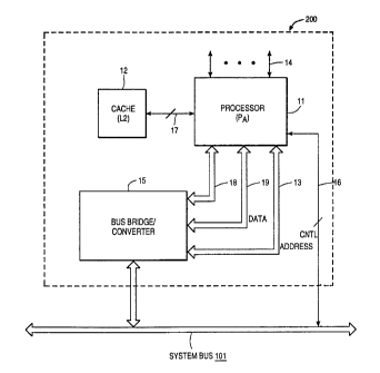
Referring now to Figure 2, there is shown a high-level, block diagram of
one embodiment of the present invention. In the embodiment of Figure 2, a
plurality of integrated circuit devices is mounted or housed on a printed
circuit
board (PCB) card (or module) 200. Card 200 includes a processor 11 coupled to
one or more cache memories 12 along lines 17. Also included on card 200 is a
bus conversion device 15 that is connected with processor 11 via lines 18, 19
and
13. Bus conversion device 15, in turn, is connected to system bus 101. In the
described embodiment, system bus 101 comprises a high-performance pipelined
bus having a standardized bus interface.
Data, address and control lines 19, 13 and 16, respectively, may be
connected directly from processor 11 to system bus 101 (as shown), or
alternatively coupled through conversion device 15.
As will be described in more detail shortly, bus conversion device 15
functions to convert the bus signalling protocol and electrical
characteristics
associated with processor 11 to the signalling protocol and electrical
characteristics associated with system bus 101, and vice-versa. In this way,
information may be transferred between the processor and other agents coupled
to system bus 1 O l . (Note that signal lines 14 are intended to represent
that there
may be other inputs/output lines to processor 11 coupled to other devices
included on card 200. For example, lines 14 may include clock input signals,
operating potential supply lines, connections to additional integrated
circuits,
etc.)
CA 02209162 2001-07-26
-11-
With reference now to Figure 3, there is shown an embodiment of the
present invention in a computer system which includes multiple agents coupled
to a high-performance bus 101. In the embodiment of Figure 3, bus 101
comprises a pipelined bus having an architecture such as that designed for the
Pentium~ Pro processor. Processor card 200 is illustrated as having a
plurality of interface terminals disposed along one edge. These terminals plug
into a mated connector 201 having a slot with a set of corresponding terminal
connections. For example, this configuration may represent a daughtercard
that connects to a motherboard via an available slot within the computer
system. This structure permits high-performance bus 101 to interface to a
number of processor cards, each of which may include any of a variety of
different processors.
As can be seen, processor card 200 comprises a processor (PA) 11
coupled with cache memories 12a-12c, and also interconnected to bus 101 via
bus conversion device 15. Other devices coupled to bus 101 include bus
master 205, direct memory access (DMA) device 202, I/O devices) 207,
expansion devices 203 and a group of processors (PB) organized into a cluster
206. By way of example, processors PB may comprise Pentium~ Pro
processors compatible with the bus architecture of pipelined bus 101. Thus, a
multiprocessor (MP) system is illustrated in the computer system of Figure 3.
For purposes of the following discussion, high-performance bus 101 may
be taken to designate the Pentium~ Pro processor bus of Intel Corporation. The
signalling protocol associated with the Pentium~ Pro processor bus is set
forth
in the publication, "Pentium~ Pro Processor Family Developer's Manual,
CA 02209162 2001-07-26
-12-
Volume 1: Specifications" (1996), which publication is available from Intel
Corporation by calling 1-800-879-4683. To better understand certain aspects of
the
present invention, however, various attributes of the Pentium~ Pro processor
bus will be discussed as they pertain to the invention.
To begin with, it should be understood that according to the bus arbitration
protocol of the Pentium~ Pro processor bus, there are two classes of bus
agents:
symmetric agents and priority agents. Symmetric agents support fair,
distributed
arbitration using a round-robin (i.e., circular priority) algorithm. Each
symmetric agent
has a unique agent identification (ID) that is assigned at RESET; a rotating
ID value
that reflects the symmetric agent with the lowest priority for the next
arbitration event;
and a symmetric ownership state indicator that indicates either a "busy" or an
"idle"
state. In the embodiment of Figure 3, for instance, processor card 200 appears
as
one of several symmetric agents coupled to bus 101.
In a typical system configuration, such as that shown in Figure 3, symmetric
agents may include devices such as processors Pg, organized individually or
into a
cluster X06, bus master 205, and various expansion devices 203, shown coupled
to
bus 101. In the computer system of Figure 3, direct memory access (DMA) device
202 may function as a high priority agent since it normally requires a direct
path to
memory. In other configurations, the priority agents) may comprise a high
priority
arbiter that arbitrates on behalf of multiple I/0 devices, as depicted by I/0
block 207 in
Figure 3.
CA 02209162 2001-07-26
-13-
An arbitration event is the process by which a new symmetric bus owner
is determined and changed. On every arbitration event, the symmetric agent
with the highest priority becomes the symmetric owner. Note that the symmetric
owner is not necessarily the overall bus owner since a priority agent, having
a
higher priority than any symmetric owner, may grab ownership of the bus from a
symmetric agent. Once the priority agent arbitrates for the bus, it prevents
the
symmetric owner from entering into a new request phase unless the new
transaction is part of an ongoing bus locked operation. Bus locked operations
are atomic operations which cannot be interrupted. An example ~of such a bus
operation is a read-modify-write cycle.
With reference now to Figure 4, there is shown a conceptual block
diagram of one embodiment of the bus conversion device 15, previously shown
in Figures 2 & 3. Dashed lines 10 and 100 represent the bus signal interface
between converter 15 in both processor 11 and bus 101, respectively.
Practitioners in the art will understand that each of interfaces 10 and 100
may
include data and address latches, voltage translations circuits, signal
conversion logic, etc., as necessary for translating and converting the
voltage
and logic levels associated with each of the respective bus interfaces.
In the case of bus interface 100, which interfaces to pipeline bus 101,
included therein is a interface unit in-order queue (IOQ) 70. The IOQ 70 is a
standard logic block associated with the PentiumOO Pro processor bus which
keeps track of the current state of bus 101. All bus agents maintain identical
IOQ status to track every transaction that is issued to the bus. When a
transaction is issued to the bus, it is also entered in the IOQ of each agent.
CA 02209162 1997-06-27
-14-
The depth of IOQ 70 is the limit of how many in-order transactions can be
outstanding on the bus simultaneously. Because transactions receive their
responses and data in the same order as they were issued, the transaction at
the top of IOQ 70 is the next transaction to enter the response and data
phases.
After completion of the response phase, a transaction is removed from the IOQ.
The IOQ is also responsible for sending signals such as HIT#/HITM#, DRDY#,
DBSY#, as well as other bus protocol signals. The default depth of the IOQ is
eight; however, bus agents may configure IOQ 70 to a depth of one by
activation of pin A7# on RESET#.
Included within bus conversion device 15 is a bus arbitration converter
(BAC) 60 that converts the arbiter signals associated with the different bus
protocols. For example, BAC 60 allows processor 11 to gain control or
ownership over pipelined bus 101 by having its arbiter signals properly
converted to the bus protocol associated with bus 101.
A detailed block diagram of bus arbiter converter 60 is illustrated in
Figure 5. Included within BAC 60 are agent identification (ID) determination
state machines 61, symmetrical owner determination state machine 62, halt
assertion logic 63, and bus request logic 64. It is appreciated that in the
symmetric arbitration scheme of system bus 101, each agent requesting access
to the bus must assert an appropriate request (BREQ#) signal. For example,
processor 11 may indicate its intention to send a request to bus 101 by
driving
the BREQ# signal line in accordance with the bus protocol of processor 11.
The signals BREQ, LOCK#, and HLDA are input to processor 11 from
bus request logic 64. (Note that each signal that assumes a logic low state
CA 02209162 2001-07-26
-15-
when asserted is followed by the pound sign, #. By way of example, the
LOCK# signal is asserted low when processor 11 is performing an atomic
transaction.)
The BREQ signal is the bus request output asserted by processor 11 to
S inform bus request logic 64 that it needs to obtain ownership of bus 101 in
order
to perform a bus cycle. The HLDA signal is a hold acknowledge output
asserted by the processor 11 to inform other requesting devices that it no
longer
owns the bus. According to the bus protocol associated with processor 11,
HLDA is not asserted until all outstanding bus cycles (i.e., that have been
previously pipelined) have completed. The bus request logic 64 converts the
bus request signal generated by processor 11 into the BREQ#[O] signal
compatible with the bus request signal associated with the protocol of system
bus 101.
In one embodiment, bus arbiter converter 60 gains ownership of bus 101
as a symmetric agent in accordance with the round-robin arbitration scheme
implemented on the Pentium~ Pro processor bus. In order to properly connect
to bus 101, each symmetric agent must be assigned a symmetric agent
identification (ID). This is the purpose of agent ID determination finite
state
machine 61. Upon power-on or reset, symmetrical agent ID determination state
machine 61 receives the BREQ#[3:0] signal lines so as to determine the agent
ID assignment of processor card 200. The agent ID information is provided to
the symmetrical owner determination state machine 62.
To gain ownership of system bus 101, the symmetric agent BREQ#[O]
signal is asserted and the symmetrical owner determination state machine 62
CA 02209162 1997-06-27
-16-
examines the state of the bus to figure out when ownership may be obtained as
a symmetric agent in accordance with the bus protocol of the Pentium ProTM
processor bus. The bus arbitration signals associated with system bus 101
include BREQ#[3:0], BPRI#, LOCK# (shown in Figure 7), and RESET#. The
BREQ#[3:0] bus signals are connected to the symmetric agents -- including bus
conversion device 15 of processor card 200 -- in a rotating manner. This
arrangement initializes every symmetric agent with a unique Agent ID during
power-on or RESET. Bus request signals BREQ#[3:0] provide a mechanism by
which individual symmetric agents send and receive bus ownership requests to
arbitrate for ownership of a system bus 101.
The BPRI# signal is a priority request signal whereby a symmetric agent
receives bus ownership requests from a high priority bus agent. For example,
BPR1# may be asserted by a priority agent so that it can arbitrate for
immediate
ownership of bus 101. The symmetric agents coupled~o bus 101 receive the
BPRI# signal as an indication that a priority agent is requesting ownership of
the bus.
Upon an arbitration event on bus 101, processor card 200 may become
a symmetric owner of the bus if it currently has the highest priority in the
system.
A priority agent may subsequently request the bus and obtain ownership over
processor card 200. For example, I/O device 207 (see Figure 3) may obtain
ownership of the bus from daughtercard 200 by asserting BPRI#, unless, of
course, processor card 200 is performing an atomic transaction and has
asserted the LOCK# signal. Processor card 200, of course, may be designated
a priority agent in an alternative embodiment.
CA 02209162 1997-06-27
-17-
Hold assertion logic 63 is coupled to receive the BPRI# signal from bus
101 and generate HOLD and AHOLD signals input to processor 11. When the
BPRI# signal is asserted on the bus 101, this means that a high priority agent
is
intervening to obtain ownership of the bus. In response to the BPRI# signal,
hold assertion logic 63 informs processor 11 not to issue any more requests.
Note that the AHOLD (address hold) signal causes processor 11 to
cease driving its address bus, so that the processor is unable to control bus
cycles. Therefore, driving the HOLD and AHOLD signals allows bus conversion
device 15 to operate with other symmetric agents on bus 101. This forces
processor 11 to not own the bus by default, whereas, in the bus architecture
of
the Pentium~ processor, the processor owns the bus by default. In a system
configuration with multiple processors or agents, use of the HOLD and AHOLD
signals eliminates the possibility of two or more processors backing off each
other, thereby leading to a "live lock" situation.
Bus request logic 64 also generates the BOFF# signal input to processor
11 to cause processor 11 to immediately release control of the bus in the
event
that a high priority agent requests ownership of the bus using the BPRI#
signal.
After the BOFF# signal is removed, processor 11 restarts the entire bus cycle.
!n an alternative embodiment, processor card 200 functions as a high
priority agent, instead of a symmetrical agent, in the computer system.
With reference now to Figures 4 & 6, bus conversion device 15 further
comprises outgoing request converter (ORC) 20 which converts requests
generated by the processor 11 to issue on system bus 101. In an exemplary
embodiment, once ownership of bus 101 has been obtained by the Pentium0
CA 02209162 2001-07-26
-1S-
processor, the outgoing request encodings must be translated from the protocol
of the Pentium~ processor to the signalling protocol of the Pentium~ Pro
processor bus 101. Further, the Pentium~ Pro bus implements a two-clock
request cycle, whereas the Pentium~ processor operates with only one clock
cycle. Therefore, ORC 20 is responsible for properly sequencing requests
issued by processor 11 as well as converting to different request type pins
from
the Pentiums to the Pentiums Pro processor bus.
Outgoing request converter 20 includes request cycling finite state
machine 21, request encoders 22 and 23, and attribute encoder~26. The
request cycling state machine 21 receives a signal on line 66 from BAC 60
indicating that processor 11 has obtained ownership of bus 101. At this point,
processor 11 may assert its ADS# (address status) output signal to indicate a
valid address and bus cycle definition are present.
State machine 21 utilizes this information to generate control signals
coupled to multiplexer circuitry circuits 24 and 25 for the various request
and
encoding changes so that the single cycle processor requests can be properly
sequenced as two separate clock cycles on system bus 101. The encoding for
the two request cycles is performed by blocks 22 and 23, which receive as
inputs the write/read (W/R#) signal, the memory or I/O transaction (M/10#)
signal
and the bus cycle definition (CACHE#) signal from processor 11. The CACHE#
signal is asserted by the processor during cache write-back cycles, and also
to
notify external memory that the processor wishes to perform a cache line-fill
using a burst bus cycle.
CA 02209162 2001-07-26
-19-
In addition, request encoder 22 receives the D/C# (data/code) signal to
indicate the type of read operation requested.
The encoded output signals produced by blocks 22 and 23 are input to
multiplexes 24. The output selected from multiplexes 24 is controlled by the
request cycling state machine 21, as shown in Figure 6. When an ADS#
signal is issued onto bus 101 by request cycling state machine 21, the various
request types from processor 11 are encoded during the first cycle by encoder
22. At this time, address signals provided by processor 11 are selected for
output onto the system bus address lines, A# [35:3J, via multiplexes 25. Basic
information about the request type is also placed onto the system bus 101 via
the REQ#[4:0] lines during the first cycle. Request encoder 22 may be
implemented using ordinary combinatorial logic that converts the Pentium~
type pins into appropriate request-type signals on the Pentium~ Pro processor
bus, according to one embodiment of the present invention.
During the second clock cycle, multiplexes 24 selects the Reqb[4:0]
output of encoder 23 for output onto the system bus 101. Also during the
second cycle, the address signal lines are utilized to send additional
information about the request type to the pipelined bus. This information
includes various attributes of the request type such as the byte enable signal
lines (BE#[7:0]); a split cycle (SCYC#) signal that notifies logic that the
locked
transfer request is twice the number of bus cycles expected; the page write-
through (PWT) signal that specifies whether the L2 cache should use a write-
back or write-through policy for the line being written to; and the CACHE#
CA 02209162 2001-07-26
-2 O-
signal. This information is selected as the output onto the address lines of
system bus 101 by multiplexer 25 during the second cycle.
In a system configuration which includes a responding agent capable of
deferring a transaction (i.e., causing it to complete out-of-order) ORC 20
should
include logic that de-asserts the DEN# signal line with each request issued on
bus 101. The DEN# signal is the defer-enable signal, and is driven on bus 101
on the second clock of the request phase on the EXF1 #/Ab4# pin (i.e., bit 4
of
the second cycle address pins). This signaling logic, for example, may be
included in the ordinary combinatorial logic of state machine 21. De-asserting
DEN# with each outgoing request prevents any responding agent from
deferring a transaction.
Address parity and request parity signals are also generated by blocks
27 and 28, respectively, onto bus 101 as part of an outgoing request.
Bus conversion device 15 further includes a bus lock converter {BLC)
circuit 50 that enables the bus to be locked during atomic transactions; that
is,
transactions over several clock cycles that cannot be interrupted. Although
the
lock protocol for the Pentium~ processor is similar to the lock signaling
protocol
implemented on the Pentium~ Pro processor bus, exactly when a lock can be
asserted in relation to the respective bus protocols varies.
Figure 7 illustrates a bus lock converter comprising a lock conversion
finite state machine 51 that receives a LOCK# signal from processor 11, as
well
as an input from ORC 20. In system bus 101, the LOCK# signal is a bi-
directional signal bused among all agents. According to the bus arbitration
CA 02209162 2001-07-26
-21-
protocol of the Pentium~ Pro processor, a current bus owner may assert
LOCK# to define an indivisible bus locked operation.
Shortly after processor 11 asserts its LOCK# signal, system bus 101
receives the translated LOCK# signal from the lock conversion state machine
according to the signaling protocol of bus 101. State machine 51 basically
implements a variable delay -- waiting for signals such as ADS#, etc., to be
generated by ORC 20 before it asserts the corresponding LOCK# signal on bus
101. The LOCK# signal on bus 101 lasts through the series of atomic
transactions and then is deasserted after the transactions have been
completed. Again, the de-assertion is performed in accordance with the
appropriate signaling protocol of bus 101.
As can be seen in Figure 4, bus conversion device 15 also includes an
incoming request converter (IRC) 30 for converting signal requests on the
system bus into signals that can be input into processor 11. According to the
signaling protocol of the Pentium~ processor, an external address strobe
(FADS#) signal is asserted to tell the processor that a valid address is
present
on its local address bus, and that this address can be snooped. When the
snoop is activated, the processor transfers the memory address from the bus to
the cache directories and a look-up takes place. But because the Pentium
ProTM processor bus does not include an EADS# signal, or its equivalent, the
present invention implements the following scheme.
Since pipelined bus 101 is commonly a multi-agent system bus, an
ADS# signal on the bus indicates a request by one of the multiple agents. All
agents coupled to the bus simply observe these requests, and, depending upon
CA 02209162 2001-07-26
_77_
the request type, determine whether it is appropriate to snoop bus 101, and
also what to do with the information.
As shown in Figure 8, IRC 30 includes an incoming request conversion
logic block 31 that receives request signals REQ#[4:0] from system bus 101.
Logic block 31 also receives ADS# signal from bus 101. Incoming request
conversion logic 31 functions to determine if a request on bus 101 is
snoopable
by processor 11. If the current transaction on system bus 101 is snoopable,
logic block 31 causes EADS# to be driven into the processor along with the
address information. Note that 1RC logic block 31 controls tri-state buffers
33
and 34 to assert/de-assert the EADS# signal and the address pins of processor
11.
Incoming request conversion logic block 31 also generates the invalidate
(INV) signal to direct processor 11 to either leave the cache line valid, or
to
mark it invalid in the case of a snoop hit. In the event that the cache line
contains valid data, the line is placed in a Shared cache coherency state.
Note
that logic block 31 should make sure that the address hold (AHOLD) signal is
asserted so that processor 11 can properly snoop the address bus. This
insures that cache consistency is maintained.
At this point it should be understood that the implementation of IRC 31
shown in Figure 8 assumes that system bus 101 has been de-pipelined for
purposes of signal convention. In alternative embodiments of the present
invention, it may be desirable not to de-pipeline bus 101. In such an
implementation, bus conversion device 15 would further include a queuing
CA 02209162 1997-06-27
-23-
mechanism that would send all snoops to processor 11 while periodically
stalling system bus 101.
Also note that IRC 31 includes snoop control logic which prevents 36-bit
requests on system bus 101 from being sent to the processor interface. For
S example, the Pentium~ processor is limited to 32-bit requests. Therefore,
IRC
logic block 31 insures that requests which are greater than 32-bits are not
snooped by processor 11.
Figure 9 is a detailed diagram of the cache coherency control unit
(CCC) 40 shown in the bus conversion device 15 of Figure 3. The
embodiment of Figure 9 shows CCC 40 comprising snoop result conversion
state machine 41 coupled to dirty data buffer 42, which, in tum, drives the
data
bus through tri-state buffers 43. Once IRC 31 has signaled to state machine 41
that a snoop has been driven into processor 11, a few clocks later the
processor
provides signals to CCC 40 indicating that either a cache hit, a cache hit to
a
dirty line, or a cache miss has occurred. This information is signaled via
signal
lines HIT/HITM and ADS.
Snoop result conversion state machine 41 also communicates with the
input-order queue (IOQ) associated with bus 101. The IOQ monitors the system
bus and sends appropriate signals to the state machine and tristate buffer 43
so
that the data may be transferred to bus 101 in accordance with the signaling
protocol of bus 101. In one embodiment, IOQ comprises ordinary bus state
tracking logic. The bus state tracking logic simply presents state information
at
the correct time via system bus 101.
CA 02209162 1997-06-27
-24-
In one embodiment, IOQ comprises a plurality of entries wherein each
entry translates to a current transaction on the pipelined bus. Each IOQ entry
tracks the state of the transaction as well. In this manner, all bus agents
may
keep track of each transaction as it flows through the pipeline on the bus.
For
the presently described embodiment, the IOQ has a depth of "1" since the bus
is
de-pipelined for conversion to processor 11.
State machine 41 also communicates some of the information from the
snoop event back to the bus tracking logic of system bus 101. In the event of
a
hit to a clean line, or a cache miss, state machine 41 simply reports this
status to
system bus 101 at the appropriate time. But if a hit occurs to a dirty line
(i.e., the
processor asserts HITM signal), this situation requires special handling since
processor 11 is designed to immediately output dirty data.
When an ADS# signal is detected by state machine 41 following a snoop
hit, this means that dirty data will be immediately sent out by processor 11.
Since the signaling protocol of system bus 101 does not allow data to be
dumped in this manner, dirty data buffer 42 captures the data as it is output
from
processor 11 so that it could be sent onto bus 101 at the appropriate time.
This
process is, of course, under the control of snoop result conversion state
machine 41. The bus state tracking logic in the IOQ is also coupled to dirty
data
buffer 42 in the implementation of Figure 9 since it has the information
indicating when dirty data may be sent on system bus 101 to complete the
transaction.
Alternatively, snoop result conversion state machine 41 may use the
BRDY# signal to throttle the data being output by processor 11. In this
CA 02209162 1997-06-27
-25-
alternative implementation, buffer 42 may be eliminated, and the data bus
lines
from processor 11 may simply by tri-stated by tri-state devices 43 before
being
coupled to system bus 101. Note that in this embodiment, BRDY# is used to
indicate that the currently addressed device has accepted data from the
S Pentium~ processor in response to a write. In other words, snoop result
conversion state machine 41 operates to allow data to be transferred directly
to
system bus 101 by providing an appropriate handshake signal.
To reiterate, logic block 41 takes the snoop result from processor 11 and
passes it to the IOQ, which is incorporated in bus interface 101. In the event
that a HITM# signal is asserted by processor 11, snoop result conversion state
machine 41 waits until the next ADS# signal has been output by processor 11,
since that signals the beginning of the dirty data dump.
Figure 10 illustrates the bus request protocol conversion logic unit 70,
which comprises ordinary state machine and combinatorial logic. As shown,
logic unit 70 includes bus protocol conversion finite state machine 72 and in-
order queue 71. State machine 71 performs required protocol signal
conversion between processor 11 and system bus 101. In-order queue 71 is
utilized to keep track of the state of both buses, on opposite sides of the
interface. IOQ 71 includes ordinary logic and register storage for holding bus
state information, as specified in accordance with the protocol of system bus
101.
In addition to tracking the state of the signals shown on both sides of the
bus interface, logic unit 70 also provides necessary handshaking signals,
e.g.,
data transfer handshaking. (Note that in certain instances, the bus signals on
CA 02209162 1997-06-27
-26-
opposite sides of the interface have closely related functions. For example,
the
ADS# signal coupled to processor 11 is a uni-directional address strobe
signal.
The corresponding conversion is to the ADS# signal of system bus 101, which
is bi-directional in nature.)
As can be seen, bus tracking logic unit 70 converts various signals
transmitted between system bus 101 and processor 11. Included within this
group is the address parity error signal AERR# in accordance with one
embodiment of the present invention. An agent detecting a parity error asserts
the AERR# signal during the error phase of the transaction. All bus agents
observe the AERR# and on the next clock abort the erroneous transaction by
removing the transaction from the in-order queue and canceling all remaining
phases associated with the transaction. The corresponding address parity
signal on the processor side of the interface is APCHK#. In the event of an
address parity error, processor 11 activates APCHK#.
Also included on the system bus side of the interface of logic unit 70 are
signals HIT#/HITM#. HIT# and HITM# are used to indicate that a line is valid
or
invalid in the snooping agent, whether the line is in the modified (dirty)
state in
the caching agent, or whether the snoop phase needs to be executed. The
HIT# and HITM# signals are used to maintain cache coherency at the system
level. As explained previously, when a snooping agent asserts H1TM# the
agent assumes responsibility for writing back the modified line during the
data
phase (an implicit write-back). The DEFER# signal is also driven in the snoop
phase. The DEFER# is deasserted to indicate that the transaction can be
guaranteed in-order completion. An agent asserting DEFER# ensures proper
CA 02209162 1997-06-27
-27-
removal of the transaction from the IOQ 71 by generating the appropriate
response. The response signal group of a transaction occurs after a snoop
phase of the same transaction and includes the signals RS#[2:0] which provide
encodings describing the required snoop result. The response agent is the
agent responsible for completing the transaction at the top of the IOQ 71. For
write transactions, TRDY# is asserted by the response agent to indicate that
it is
ready to accept write or writeback data.
The data transfer signal group contains signals driven in the data phase
and includes DBSY#/DRDY# (data bus busy and data ready). DRDY#
indicates that valid data is on the bus and must be latched. The data bus
owner
asserts DRDY# for each clock in which valid data is to be transferred. DBSY#
is
used to hold the bus before the first DRDY# and between DRDY# assertions for
a multiple clock data transfer. The snoop, response, and data phase signals
are all tracked via IOQ 71.
Bus protocol conversion state machine 72 provides outputs to
processor 11 that include the next address input (NA#). The NA# input is
asserted by a device that requests that the next bus cycle be sent over the
buses prior to the current cycle ending. The external right buffer empty
(EWBE#) signal is provided to processor 11 to ensure that memory
operations occur in order of execution (i.e., strong memory ordering). This
ensures that all buffered writes are completed by executing the next
instruction. As previously discussed, the BRDY# signal indicates that the
currently addressed device has presented valid data on the data bus pins in
response to a read, or that the currently addressed device has accepted data
CA 02209162 1997-06-27
-28-
from the processor in response to a write. Similarly, KEN# is the cache
control signal indicating whether a location being read is within cacheable
address space. If an address is not cacheable, the KEN# line is driven
inactive telling the processor not to perform a cache line-fill.