Note: Descriptions are shown in the official language in which they were submitted.
CA 02209290 2001-09-10
21766-790
1
FREQUENCY SYNTHESIZER
The application relates to a circuit for frequency
synthesis.
Such circuits are generally known. Frequency
synthesizers are thus known which comprise a digital
controlled oscillator followed by a filter. When the
digital controlled oscillator is adapted for generating more
than one frequency, the relevant filter must of course be a
tracking filter. Such so-called tracking filters are
expensive and bulky.
Such prior art circuits are moreover only suitable
for large frequency steps. Nor are they suitable for
integration into a modulator.
The object of the present invention is to provide
a circuit for frequency synthesis wherein the above
mentioned drawbacks are avoided.
This object is achieved by such a circuit which is
characterized by:
a digital controlled oscillator, comprising:
a clock generator;
an adder circuit to which the signal from the
clock generator is fed; and
a control digit feed circuit for feeding a signal
representing a control digit to the adder circuit; and
a phase-locked loop (PLL) which is connected to
the carry output terminal of the adder circuit and which is
provided with a phase detector, a low-pass filter and a
CA 02209290 2003-O1-24
21766-790
2
controlled oscillator, wherein the carry output terminal is
connected to the phase detector. It is noted here that in
the literature such a digital oscillator is also known as a
fractional rate multiplier, digital controlled oscillator,
or as accumulator circuit. The frequency of the output
signal, the carry signal, satisfies the following formula:
fcarr}~ - fsys '
Nmax
wherein:
Nmax - is the largest number which can occur in the
adder circuit;
Ni - is the control digit;
fsys - is the system frequency;
(carry - is the frequency of the carry signal.
Although a circuit as described above can easily
be embodied in integrated form and no tracking filter is
necessary due to the use of a PLL, the wave shape is found
to be not entirely optimal. This is due to the fact that -
as a result of the operation of the digital controlled
oscillator - the frequency of the output signal is not
regular.
The adder circuit is adapted to generate a
remainder-representing signal. Preferably arranged is a
CA 02209290 2001-09-10
21766-790
2a
correction circuit for deriving a correction signal from
this remainder. According to a first embodiment an output
terminal of the correction circuit is connected to a
combination circuit which is connected to the input
terminals of the phase detector.
The results are however improved even more when
the correction circuit comprises three controlled
accumulators and a digital-to-analog (D/A) converter.
The very best results are however obtained only
when the correction circuit comprises N digital controlled
accumulator circuits, wherein each of the accumulators is
adapted to receive the remainder of the preceding
accumulator and each of the accumulators is connected via a
plurality of difference determining circuits equal to its
order number - 1 to an adder circuit, the output terminal of
which is connected to the D/A converter.
CA 02209290 2003-O1-24
21766-790
3
The above described frequency synthesizer is
suitable for generating a sine-shaped signal, a saw-tooth
signal, a square wave signal or other type of signal of
which the frequency is externally controlled, for instance
for generating a signal for use in measuring equipment or in
modulators and/or demodulators.
In such an application it is therefore attractive
to integrate the modulation process or the demodulation
process in the circuit. It is assumed here that by the term
"modulate" in the accompanying claims is also understood
demodulate; both after all comprise making a non-linear
combination of the signal for processing with a carrier wave
signal.
The circuit according to the invention can be used
in frequency or phase modulation and even in amplitude
modulation. In this latter case a combination is made of
two or more phase modulators. It is of course possible to
use the circuit according to the invention in a combination
of frequency or phase modulation with amplitude modulation.
The invention may be summarized in one aspect as a
circuit, including one or more circuits for frequency
synthesis, at least one of said circuits for frequency
synthesis comprising: a first controlled oscillator which is
digitally controlled and adapted to generate a signal
representing a remainder, comprising: a clock generator; an
accumulator circuit to which the signal from the clock
generator is fed; and a control digit feed circuit for
feeding to the accumulator circuit a signal representing a
control digit; a phase-locked loop (PLL) which is connected,
via a combination circuit, to a carry output terminal of the
CA 02209290 2003-O1-24
21766-790
3a
accumulator circuit and which is provided with a phase
detector, a low-pass filter incorporated in the phase-locked
loop after the phase detector, and a second controlled
oscillator incorporated in the phase-locked loop after the
low-pass filter and before the phase detector, wherein the
carry output terminal is connected to the phase detector via
said combination circuit; and a correction circuit for
deriving a correction signal from the signal representing a
remainder characterized in that an output terminal of the
correction circuit is connected to said combination circuit
which is connected to an input terminal of the phase
detector.
According to another aspect the invention provides
circuit for frequency synthesis, comprising: a first
controlled oscillator which is digitally controlled and
adapted to generate a signal representing a remainder,
comprising: a clock generator; an accumulator circuit to
which a signal from the clock generator is fed; and a
control digit feed circuit for feeding to the accumulator
circuit a signal representing a control digit; a phase-
locked loop (PLL) which is connected, via one or more delay
circuits, to a carry output terminal of the accumulator
circuit and which is provided with a phase detector, a low-
pass filter incorporated in the phase-locked loop after the
phase detector, and a second controlled oscillator
incorporated in the phase-locked loop after the low-pass
filter and before the phase detector, wherein the carry
output terminal is connected to the phase detector via said
one or more delay circuits; and a correction circuit for
deriving a correction signal from the signal representing a
CA 02209290 2003-O1-24
21766-790
3b
remainder, comprising: N accumulator circuits, wherein the
first of said N accumulator circuits is adapted to receive
said signal representing a remainder, and each of the N
accumulator circuits after the first is adapted to receive a
remainder of the preceding accumulator circuit in the
correction circuit, and each of the N accumulator circuits
is connected to an adder circuit via a plurality of
difference determining circuits equal to an order number of
the accumulator circuit in the correction circuit minus 1;
and a digital-to-analog (D/A) converter connected to an
output of said adder circuit; characterized in that an
output terminal of the D/A converter of said correction
circuit is connected to a second adder circuit incorporated
in the PLL after the phase detector.
The invention will be further elucidated
hereinbelow with reference to the annexed drawings, wherein:
figure 1 shows a diagram explaining the operation
of a digital controlled oscillator;
figure 2 shows a phase spectrum of the signal
generated by the digital controlled oscillator;
figure 3 shows a frequency spectrum of the signal
generated by the digital controlled oscillator;
figure 4 shows a diagram of a first embodiment of
a circuit according to the invention;
figure 5 shows a diagram of a second embodiment of
a circuit according to the invention;
CA 02209290 2003-O1-24
21766-790
3c
figure 6 shows a circuit according to the
invention which produces a signal with a better qualtiy
through the choice of control digits and ratios;
figure 7 shows a circuit according to a third
embodiment of the invention;
CA 02209290 1997-07-03
WO 96!21279 PCT/NL96/00013
4
figure 8 shows a circuit according to the invention
which is adapted for phase or frequency modulation;
figure 9 shows another embodiment of a diagram which
is suitable for phase or frequency modulation;
figure 10 shows a diagram of a circuit according to
the invention adapted for phase modulation;
figure 11 shows a phaser diagram to elucidate the
principle of the circuits for amplitude modulation shown
in figure 12;
figure 12 shows a diagram of a circuit according to
the invention suitable for amplitude modulation; and
figure 13 shows a diagram of a circuit according to
another embodiment according to the invention, with which
multiple modulation is possible.
For an understanding of the present invention it is
important to understand the operation of a digital con-
trolled oscillator. The circuit and the operation of a
digital controlled oscillator is thus first elucidated
with reference to figure 1.
The digital oscillator 1 shown in figure 1 is formed
by a register 2 to which a clock signal with the frequen-
cy f8Y8 is supplied via a clock signal line 3. The register
is connected on its input side to a digital adder circuit
4, while the likewise parallel output terminal of the
register is connected to one of the two input terminals
of adder circuit 4. Connected to the other input terminal
of adder circuit 4 is a control digit register circuit 5.
The output terminal of the register is also embodied
separately. It is of course also possible to vary the
content of the control digit register 5 from outside. In
the wording of the claims the combination of adder
circuit and register is referred to as accumulator.
The operation of this control digit circuit is as
follows: in the adder circuit 4 the content of the con- '
trol digit register 5 is added to the content of the
register prior to the preceding clock cycle. The result
of this addition is fed to the register 2. This addition
is herein performed modulo a determined number. This
CA 02209290 1997-07-03
WO 96/21279 PCT/NL96/00013
determined number will correspond to the maximum content
of the register, in general thus a power of 2. Thus, for
each addition which exceeds this power of two, for in-
stance 8, a carry signal results which essentially forms
5 the output signal of the digital controlled oscillator.
Only when in the result of an addition the maximum con-
tent is not reached is no carry signal generated. Thus,
in the case the dividend is 7 and the maximum content of
the register is 8, a carry signal is generated seven of
the eight times a clock pulse is supplied.
It will be apparent that the thus obtained output
signal is subject to serious phase errors. Expressed in
time these phase errors lie in the range between 0 and
1/f
. The starting point here is the situation where the
sYs
reference level lies at a limit of the range over which
the phase errors are distributed; it is likewise possible
to place the reference point in the middle of this range
and to let it extend to both sides. The maximum phase
error is then of course a factor of 2 smaller, but this
can be positive as well as negative.
This is all shown in figure 2. The output signal is
therefore affected by a phase error and it is possible to
depict this phase error in the frequency range. This
results in figure 3.
In figure 3 the rectangular characteristic shows the
distribution of the frequency of the digital oscillator.
It can be seen here that these frequencies extend between
0 and twice the generator frequency. Little can be said
however about the distribution hereof. The drawing is
therefore limited to a uniform distribution. The object
is of course to generate only the actual target frequen-
' cy, F
. There are in principle three possible ways of
gen
doing this:
' A) lowering all frequencies except for the desired
frequency,
B) suppressing the frequencies around fgen in the
direct vicinity hereof; further operation can then take
place with a filter,
CA 02209290 1997-07-03
WO 96/21279 PCT/NL96/00013
6
C) a priori only generating the desired frequency.
The resulting frequency spectra are designated with
A respectively B in figure 3.
r
A first embodiment of the invention will now be
shown with reference to figure 4, which embodiment fol-
a
lows the strategy designated under rrA~~ above.
The circuit is formed by a digital controlled oscil-
lator 8 to which a clock signal is fed via a clock signal
line 9 and to which via N parallel lines 10 a control
digit is fed in digital form. The digital controlled
oscillator has two output terminals. At a first output
terminal a digital signal becomes available, the frequen-
cy of which is the same as the frequency presented by the
control digit.
This signal is fed via a combination circuit 17 to a
phase detector 12 which forms part of a phase-locked ~n~n
y _ y____ -_____~ ___r.
13. The phase-locked loop comprises a voltage-controlled
oscillator 14 and a low-pass filter 15. It is noted here
that under voltage-controlled oscillators are also under-
stood current-controlled oscillators. The output signal
of the phase detector is fed to the low-pass filter 15,
the output signal of which controls the voltage-con-
trolled oscillator 14. The output signal of the voltage-
controlled oscillator 14 becomes available at an output
terminal 16 and is also fed to a second input terminal of
the phase detector 12. Further arranged between the phase
detector and the low-pass filter is the analog adder
circuit 14a.
The digital controlled oscillator is further provid-
ed with a second output terminal 18 at which the remain-
der of the addition performed by the digital controlled
oscillator is available. This remainder is fed to a '
correction circuit 19, the output terminal of which is
connected to a combination circuit 17.
The operation of the circuit will be explained
hereinbelow.
The digital controlled oscillator acts initially as
an adder. The clock signal 9 coming from a crystal oscil-
CA 02209290 1997-07-03
WO 96121279 PCT/NL96/00013
7
lator not shown in the diagram is added by the adder
circuit 8 in the digital controlled oscillator, wherein,
in order to bring about optimum operation of the oscilla-
tor, the counting preferably takes place until an "ugly"
number is obtained. By an "ugly" control digit is under-
stood a control digit which, when divided by the overflow
number, produces a poorly divisible fraction; in other
words, that as few factors as possible occur in common in
both numbers. Reference is otherwise made herein to the
formula on page 2. This will result in a ratio between
the frequency of the output signal of the voltage-con-
trolled oscillator and the clock signal fed thereto,
wherein as few components of the clock signal as possible
are to be found in the output signal, which is of the
utmost importance for further processing of the signal.
The output signal is fed to the phase-locked loop
which removes possibly remaining unwanted frequency
components.
This is related to the fact that the output signal
of the digital controlled oscillator is a square wave,
which, as a result of the operation of the digital oscil-
lator, is not entirely regular, so that this square wave
comprises a high percentage of undesired, non-harmonic
components which must of course be filtered out. This
filtering takes place by means of a phase-locked loop.
The output signal of the phase-locked loop is there-
fore substantially sine-shaped or of other shape without
further components.
The correction switch 19 therefore has as its most
important function to correct the phase of the output
signal by using as correction term the remainder present
on the digital controlled oscillator 8. A D/A converter
21 is of course necessary for this purpose, since the
" remainder is a digital form and the phase-locked loop is
a circuit with analog operation.
According to an embodiment not shown in the drawings
a divider circuit is arranged between the voltage-con-
trolled oscillator and the phase detector. The use of the
CA 02209290 1997-07-03
WO 96/21279 PCT/NL96/00013
8
described divider circuit creates the possibility of
reducing the time error. When the divider circuit has a
divider M, time resolution can be improved by a factor M.
A shift register-like circuit is herein used which in
fact forms an implementation of the combination circuit
17. The shift register-like construction can be clocked
with a multiple of the system frequency or with the
frequency generated by the voltage-controlled oscillator
or with a signal derived from said frequency with a
divider. Use can also be made of an oscillator of which
the system clock is derived from a divider circuit. The
resolution is then FgYs/M, herein TSYS = 1/fgYB.
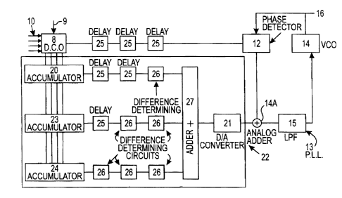
Figure 5 shows a second embodiment of the frequency
synthesizer according to the invention wherein the cor-
rection circuit has a different configuration. In the
figure only the analog adder circuit 14 is designated,
while the combination circuit 17 (not shown) can also be
used, either in combination or not. This is the configu-
ration according to model B in figure 3.
The correction circuit 22 according to this second
embodiment comprises a digital accumulator 20 followed by
a second digital accumulator 23 and a third digital
accumulator 24. In terms of circuitry the accumulators
correspond with the digital controlled oscillators. The
accumulators are mutually connected herein by means of
their remainder terminals. The carry terminal of the
second accumulator is connected via two delay circuits 25
to a difference determining circuit 26. The third digital
accumulator 23 comprises a carry terminal which is con-
netted via a delay circuit 25 and two difference deter-
mining circuits 26 to a digital adder circuit 27. Final-
ly, the carry terminal of the fourth digital accumulator
24 is connected to adder circuit 27 via three difference
determining circuits 26. '
The output terminal of adder circuit 27 is connected
to D/A converter 21.
This circuit further differs from the circuit shown
in figure 4 in that three delay circuits 25 are arranged
CA 02209290 1997-07-03
WO 96!21279 PCT/NL96/00013
9
between the digital controlled oscillator 8 and the phase
detector 12 of the phase-locked loop 13. These circuits
are of course provided with clock terminals (not shown in
the drawing) for synchronization purposes.
The operation of this circuit differs relative to
the circuit shown in figure 1 in that the approximation
of the correction term supplied to the phase-locked loop
is three orders of magnitude better. In the phase domain
this amounts to a drop of 20 dB/decade per accumulator.
This will of course result in a better frequency stabili-
zation. It will be apparent that it is possible to change
the number of digital accumulators in the correction
circuit, for instance by only using two. In that case one
of the delay circuits 25 connected to the digital accumu-
lator 20 is omitted, as is the delay circuit 25 connected
to the digital accumulator 23 and one of the delay cir-
cuits connected between the first digital controlled
oscillator 8 and the phase detector 12. Of course it is
also possible to increase the number of digital accumula-
tors to make the approximation more accurate. All these
embodiments fall within the scope of the present inven-
tion even though they are not shown in the drawings. The
choice of which depends on the accuracy the output signal
is required to satisfy.
It is possible to employ a configuration wherein the
correction signal comprises two parts which each process
a part of the remainder and one of which adds a first
correction signal to the signal from the digital oscilla-
tor and the second supplies a second correction signal to
the phase-locked loop. (Such a configuration is a combi-
nation of the models A and B).
Shown in figure 6 is another embodiment which falls
under the designation C in figure 3. Herein two combina-
tions, each of a digital controlled oscillator and a
phase-locked loop, are connected in cascade. Each of the
digital controlled oscillators is provided with a control
digit input terminal. It is of course possible to connect
in cascade more than two of such combinations. It is of
CA 02209290 1997-07-03
WO 96/21279 PCT/NL96/00013
course possible to freely select the divisions of the
digital controlled oscillators which perform the frequen-
cy division. The first digital controlled oscillator 28
changes the feYa which is presented at its input terminal
5 by a factor as according to the formula on page 2, where-
in the first PLL only allows through signals located in
the direct vicinity of the frequency of fsY$ times the
divider of the first digital controlled oscillator. By
again using the combination of a digital controlled
10 oscillator and a phase-locked loop an improvement in the
thus obtained signal is achieved ir. respect of phase
purity and frequency. This provides a large number of
degrees of freedom, wherein it is noted that, particular-
ly when control digits are used which are related to each
other as little as possible, a signal is obtained which
is as "clean" as possible. According to this embodiment
an oscillator is thus obtained of which the frequency is
freely adjustable and of which the quality of the output
signal is high.
Shown in figure 7 is a third embodiment with which
an even better freedom from fitter can be obtained.
As in the foregoing embodiments, this circuit com-
prises a controlled oscillator, which in this embodiment
is formed by three blocks 8, 42 and 43 and a phase-locked
loop which is designated in its entirety by 13. The
output terminal of block 8 is also connected to a correc-
tion circuit 19 which is connected to the phase-locked
loop 13. However, in contrast to the foregoing embodi-
ment, correction circuit 19 is connected to a delay
circuit 41 which is incorporated in the phase-locked loop
and which can take the form of a frequency divider.
The digital controlled oscillator is thus formed by '
three parts. This is comparable to for instance a prior
art 1000-counter; this can be defined as a 10-divider
concatenated with a 100-divider. It is thus also possible
to combine for instance hexadecimal and decimal numbers,
such as a number that consists of two hexadecimal and
three decimal positions. The three decimal positions may
CA 02209290 1997-07-03
WO 96!21279 PCT/NL96/00013
11
be taken together and then obtain a "MOD 1000" operation.
The two hexadecimal positions together obtain a "MOD 256"
operation.
Our digital oscillator is also split In this manner;
a block 8 which indicates a remainder, a block 43 which
indicates a number of times n (or 180) and a block 42
which indicates a number of times ~r/A.
In order to bring about good concatenation this
latter block performs a modulo A operation; A pieces of
~r/A equals ~r, i.e. block 43 is increased by 1 if the
modulo operation has sufficient space. In short, 8, 42
and 43 together form the digital controlled oscillator.
Block 42 has a content of which the value is always
smaller than A. It can thus be stated that if the value
of the 7r-signal of block 43 changes at the flank of the
clock signal, the remainder in block 42 indicates what
the error is, expressed in pieces ~r/A. If now the PLL
generates a frequency which is A times as high as the
reference signal from block 43, this frequency, expressed
in time per cycle, thus equals ~r/A. The unit of an RF
cycle and the remainder has thereby become identical;
this is useful for reducing the error in the time, which
was initially a maximum of one system cycle, to one
oscillator cycle. The voltage-controlled oscillator or
VCO will thus generate a much higher frequency than the
system clock signal, which is of course attractive.
The use of the RF clock signal itself is quite
simple; the partial remainder in block 42 (the rest of
the remainder is in block 8) indicates, expressed in one
numeral, the number of full VCO cycles in which the
reference comes too late relative to the divided down VCO
clock signal. By now delaying the divided down VCO clock
signal by the same number of cycles, the remaining error
becomes significantly smaller, i.e. as small as the VCO
clock signal.
The remaining remainder in block 8 now indicates in
a fraction of the RF cycle that there is still a residual
error. The fitter caused by this error can be decreased
CA 02209290 1997-07-03
WO 96/21279 PCT/NL96/00013
12
with an integrator or fitter shaper 46 and can then be
combined in the synchronization circuit 47 with the
signal from block 42 and be added to the delay circuit
41. The fitter shaper 46 thus ensures that the maximum
phase error of one VCO cycle can be suppressed using the
averaging of the phase error through time. This is an
important suppression function of the PLL.
The use of a variable A for the modulo operation and
the dividing operation results in an additional degree of
freedom which can be chosen by causing the digital oscil
lator to generate an "ugly" frequency. An example: say
that the VCO is supposed to generate a frequency of 320.1
MHz and that the applied system frequency is 20 MHz. It
is then extremely irritating to have A equal for instance
64 and to have to generate about 5 MHz (320/64) in the
digital oscillator. The ratio of 5 to 20 MHz is then too
much of a whole number, so that rather a lot of low
frequency fitter remains. Instead we choose for instance
54 for A, so that we must generate 320.1/54 equals 5.92
MHz. This produces much more high frequency fitter which
is much easier to eliminate.
It will be apparent that by using a division by A in
the phase-locked loop 13 as well as in the digital part
of the oscillator a sampling process is supplied at
another frequency, which of course has a favourable
effect on the stability and thus on freedom from fitter.
In accordance with a non-essential but attractive
embodiment, a low-pass filter 45 is connected between the
phase detector and the voltage-controlled oscillator, as
is typical in phase-locked loops.
The above embodiments are essentially suitable for
generating a signal with a constant frequency. It is of '
course possible to use the circuits for generating modu-
lated signals.
An embodiment hereof is shown in figure 8. A signal
representing the carrier wave frequency is herein sup-
plied to a digital adder circuit 32 via the connection 29
and the modulating frequency or the digital signal repre-
CA 02209290 1997-07-03
WO 96/21279 PCT/iVL96/00013
13
senting the modulating phase is supplied via a connection
30. The two signals are added together in the adder
circuit 32 and fed to the digital controlled oscillator
8
as control digit. It will be apparent without much expla-
nation that this circuit can be used to generate a fre-
quency-modulated signal or a phase-modulated signal. With
the circuit the phase and the frequency of the generated
signal can be extremely accurate and are only limited by
the technology used.
In the embodiment shown in figure 9 an adder circuit
35 is arranged between the digital controlled oscillator
8 and the phase-locked loop 13. In this adder circuit the
digital controlled oscillator 8 is used to generate the
carrier wave signal in digital form, wherein the modulat-
ing signal supplied via the connection 34 is added to the
carrier wave signal in adder 35 and subsequently fed to
the phase-locked loop 13. This circuit can also be used
for both phase and frequency modulation.
Figure 10 shows an embodiment wherein the modulating
signal 34 is supplied to a D/A converter 36 and the
signal is subsequently used in analog form for addition
to the signal circulating in the phase-locked loop 13.
Use is herein made of an adder circuit 37 incorporated in
the phase-locked loop 13. It will be apparent that this
latter embodiment can only be used for phase modulation.
It is however possible to add the signal to other posi-
tions in the phase-locked loop, for instance to the
signal between voltage-controlled oscillator 14 and phase
detector 12.
The above described embodiments relate to phase or
frequency modulation of a carrier wave. It is possible to
produce amplitude modulated signals by combining phase
modulated signals.
This will be clarified with reference to figure 11,
wherein phasers are shown which each represent a phase-
modulated signal and wherein the phase of both signals is
opposed and which, when added together, result in an
amplitude-modulated signal. When this is applied in
CA 02209290 1997-07-03
WO 96/21279 PCT/NL96100013
14
practice there results for instance a circuit as shown in
figure 12. Use is herein made of the phase modulation
circuit shown in figure 9, wherein two such circuits are
arranged which are each supplied with a modulating signal
in opposed phase.
The digital controlled oscillator of both circuits
can of course be combined and it is necessary to add
together the output signal of the two circuits. Use is
herein made of an analog adder circuit 38. This can be
formed for instance by an adder circuit provided with
resistors. This is however not a particularly attractive
option, since resistors are difficult to embody in inte-
grated form and they have a high dissipation, which is
less desirable particularly in battery-powered applianc-
es. It is further possible to make use of a transformer,
which is also difficult to implement in integrated form
and which has a number of limitations in the frequency
range. Another possibility is to make use of so-called
patch radiators, particularly when using high frequen-
ties. The use of three or more phase modulators to gener-
ate an amplitude-modulated signal has the advantage of
ensuring that amplitude 0 can be generated. When two
phase-modulated signals with differing amplitudes are
added together, the amplitude of the resulting signal can
never be made 0.
Finally, figure 13 shows an embodiment of a circuit
for generating modulated signals which is suitable for
generating signals which are phase- or frequency-modulat-
ed and amplitude-modulated. Use is made herein of a so-
called pre-modulation filter which derives signals from
the modulating signal supplied to pre-modulation filter
via terminal 34, which signals are suitable for fre- '
quency modulation and phase modulation, wherein the phase
modulating signals can be used for amplitude modulation.
35 This circuit corresponds with the circuit shown in figure
12 with the exception of the use of a band-pass filter 41
which is used in this embodiment because the thus modu-
lated signal is converted in frequency. The band-pass
CA 02209290 1997-07-03
WO 96121279 PCTINL96100013
filter is necessary to prevent the modulation from being
influenced by the conversion.
For a specific application methods A, B and C can be
used both alone and in combination. The degree to which a
5 method is used depends on the available technology and
the set requirements. The correct combination of methods
as well as the contribution of the method can be found by
means of an optimization procedure.
It will be apparent that various modifications can
10 be made to the circuit according to the present invention
without deviating from the invention.