Note: Descriptions are shown in the official language in which they were submitted.
CA 02209305 1997-07-02
WO 96/21902 PCT/US96/00342
SYSTEM AND METHOD FOR HIERARCHICAL DEVICE EXTRACTION
BACKGROUND OF THE INVENTION
Field of the Invention
The invention relates to automated design verification techniques for
integrated circuits, more particularly to hierarchical device extraction.
Description of Background Art
Many structures and systems are comprised of components whose
interrelations are defined by design rules. Such structures are often designed
using
automated design techniques that use symbolic representations of the structure
and
its elements. An example of such a structure is an integrated circuit.
The physical design of an integrated circuit is frequently described in terms
of
the symbolic layout of the circuit, rather than the actual geometry of the
masks and
layers that comprise the chip. When creating mask works for integrated
circuits,
designers typically begin with a circuit schematic that includes an
interconnected
network of logic or circuit elements. One or more circuit elements can be
combined
to form a device. A library of mask work patterns or "cells" that correspond
to the
various circuit devices used in the design is available to the circuit
designer. The
designer can thus work with symbolic representations of transistors, wires,
and other
primitive components, and groups of these components to form a device. These
symbolic representations provide a higher level of abstraction than the mask
layout.
Working at a higher level of abstraction simplifies the design task by
allowing the
designer to concentrate on designing with higher level devices instead of
designing
with the low level circuit elements. The use of a symbolic representation
allows the
designer to simulate and verify the logical operation of the circuit before
actual
fabrication.
A symbolic layout containing only primitive symbols, i.e. symbols
representing transistors, wires, capacitors and other physical components, is
termed
a "leaf cell." The connections between cells are called "ports." Many layouts
contain
a large number of substantially identical groups of components or devices.
Such a
group of components define a cell. The description of the layout can be
simplified by
treating each group of components as an instance of the particular cell. Each
cell is
represented symbolically. For example, a cell can be represented as a
rectangle with
various ports for connecting wires or for abutment with ports of adjacent
cells that
are similarly represented. The components of the overall layout may consist of
many
cells, and the layout represents their relative placement and interconnection.
Describing the layout in terms of cells rather than primitive symbols further
simplifies the task of the designer.
CA 02209305 1997-07-02
WO 96121902 PCT/US96/00342
The process of grouping elements and cells may be repeated so that a
symbolic layout can be treated as a hierarchical structure with multiple
levels. Each
level is a symbolic layout of cells and primitive components. Each cell is in
turn a
symbolic layout of sub-cells and primitive components. The sub-cells and
primitive
components of a "parent" cell comprise the next lower level in the hierarchy.
Since
there may be more than one type of cell at any given level, the next lower
level may
contain several different branches. The cells at the lowest level are leaf
cells since
they contain no sub-cells, only primitive components, as described above.
Cells at
any other level are "hierarchy cells." The hierarchy can be visualized as an
inverted
"tree" with branches extending downward, and the lowest level depends on the
branch in which it is located. The leaf cells are at the ends of the branches,
and the
trunk of the tree represents the symbolic layout of the whole chip, which is
often
termed the "root cell." This hierarchical description is a natural and concise
representation for large designs.
Once the symbolic layout is designed it is tested to verify its logical
functioning. Any defective operation is remedied by design changes and the
modified design is re-verified. When verifying an integrated circuit design,
each
device in the design must be extracted, i.e., located and identified. The
interconnections between the devices are then checked, and place and routing
designs are then verified.
A device is a combination of components that perform a particular function.
Device extraction is the process of locating devices within the integrated
circuit
design. Conventional verification systems require all of the device components
to be
wholly contained within one cell in order to be identified. In order to verify
an
integrated circuit design that contains cells in a hierarchical format, the
cell must be
leveled before device extraction can begin. Leveling occurs because a device
design
cannot be extracted if it is located in multiple cells. As integrated circuit
designs
become more complicated design conventional design verification tools requires
an
inordinate amount of time to verify an integrated circuit design because of
the large
number of devices.
What is needed is a system and method for extracting a device from a circuit
design in which the cells are not leveled for each device that is contained in
two or
more cells of the cell hierarchy.
SUMMARY OF THE INVENTION
In accordance with the system and method of the present invention, device
extraction from a hierarchical cell design proceeds by selecting a cell from
the lowest
level of the hierarchy and by searching the cell for the device components. A
device
extractor searches each cell in the lowest level and then selects a "parent"
cell in the
-2-
CA 02209305 2000-09-08
penultimate level. The parent cell, and all of the children cells of the
parent cell, are
searched. The selection and search process continues until all of the
components of the
device are identified in a cell and in the children of the cell and a proper
relationship between
the components is determined. The components of the identified device are
masked so that
they are not identified and associated with another device during subsequent
searches.
Accordingly, in one aspect of the present invention there is provided a method
for
extracting a first device having a recognition component and a terminal
component from a
first representation of an integrated circuit mask, the first representation
including the
recognition component and the terminal component located in two or more of a
hierarchy of
cells, a first rule defining the first device as a first relationship between
the recognition
component and the terminal component, the method comprising the steps of:
(1) selecting a first cell of the hierarchy of cells wherein all child cells
of said first
cell have been previously selected;
(2) identifying the recognition component if the recognition component is
located
in one of said first cell and a first child cell of said first cell, the
recognition component is a
shape on the integrated circuit mask;
(3) identifying the terminal component if the terminal component is located in
one
of the first cell and a second child cell of the first cell, if the
recognition component is
identified in step (2), the terminal component is a shape on the integrated
circuit mask; and
(4) extracting the first device if a relationship between the recognition
component
and the terminal component satisfies the first rule.
According to another aspect of the present invention there is provided a
method for
extracting a first device having a recognition component and a terminal
component from a
first representation of an integrated circuit mask, the first representation
including the
recognition component and the terminal components located in two or more of a
hierarchy of
cells, a first rule defining the first device as a first relationship between
the recognition
component and the terminal component, the method comprising the steps of:
(1) identifying a first group of rules each describing a relationship between
the
recognition component and one or more additional components, wherein the first
device
includes one recognition component and one or more terminal components;
(2) select the recognition component;
(3) selecting the first rule from said first group of rules;
-3-
CA 02209305 2000-09-08
(4) selecting a first cell of the hierarchy of cells, wherein all child cells
of said
first cell have been previously selected;
(5) identifying the recognition component if the recognition component is
located
in at least one of said first cell and all of said child cells of said first
cell including the step of
merging the first component if the recognition component is located in two or
more of said
hierarchy of cells, the recognition component is a shape on the integrated
circuit mask;
(6) identifying the terminal component if the terminal component is located in
at
least one of said first cell and all of said child cells of said first cell if
the recognition
component is identified in step (S), the terminal component is a shape on the
integrated
circuit mask; and
(7) extracting the first device if a relationship between the recognition
component
and the terminal component satisfies the first rule.
According to yet another aspect of the present invention there is provided a
computer
based system having a storage device for extracting a first device having a
recognition
component and a terminal component from a first representation of an
integrated circuit
mask, the first representation including the recognition component and the
terminal
components located in two or more of a hierarchy of cells, a first rule
defining the first device
as a first relationship between the recognition component and the terminal
component, the
system comprising:
a rule identifier for identifying a first group of rules each describing a
relationship
between the recognition component and one or more additional components,
wherein the first
device includes one recognition component and one or more terminal components;
a recognition component selector, disposed to receive signals from said rule
identifier,
for selecting the recognition component, the recognition component is a shape
on the
integrated circuit mask;
a rule selector, disposed to receive signals from said rule identifier, for
selecting the
first rule from said first group of rules;
a cell selector for selecting a first cell of the hierarchy of cells, wherein
all child cells
of said first cell have been previously selected;
a component identifier, disposed to receive signals from said recognition
component
selector, for identifying the recognition component if the recognition
component is located in
at least one of said first cell and all of said child cells of said first cell
including the step of
merging the recognition component if the recognition component is located in
two or
-3 a-
CA 02209305 2000-09-08
more said hierarchy of cells and for identifying the terminal component if the
terminal
component is located in at least one of said first cell and all of said child
cells of said first cell
if the recognition component is identified, the terminal component is a shape
on the
integrated circuit mask; and
a device extractor, disposed to receive signals from said component
identifier, for
extracting the first device if a relationship between the recognition
component and the
terminal component satisfies the first rule.
BRIEF DESCRIPTION OF THE DRAWINGS
An embodiment of the present invention will now be described more fully with
reference to the accompanying drawings in which:
Figure 1 is an illustration of a computer system in which the preferred
embodiment
operates.
Figure 2 is a more detailed illustration of the hierarchical device extraction
module of
the preferred embodiment.
Figure 3 is a more detailed illustration of the hierarchical access engine
module of the
preferred embodiment.
Figure 4 is a symbolic representation of a device in an integrated circuit
design.
Figures SA-SC are flowcharts showing the method of the application shell
module of
the preferred embodiment.
Figure 6 is a flowchart showing the method of the multiple access processor
module
of the preferred embodiment.
Figure 7 is a flowchart showing the method of the hierarchical access engine
module
of the preferred embodiment.
Figure 8 is a flowchart showing the method of the data-to-data processor
module of
the preferred embodiment.
Figure 9 is a flowchart showing the method of the cell-to-data processor
module of
the preferred embodiment.
Figures l0A-l OC are flowcharts showing the method of the cell-to-cell
processor
module of the preferred embodiment.
DETAILED DESCRIPTION OF THE PREFERRED EMBODIMENTS
A preferred embodiment of the present invention is now described with
reference to
the figures where like reference numbers indicate identical or functionally
similar devices.
-3b-
CA 02209305 2000-09-08
Also in the figures, the left most digits of each reference number corresponds
to the figure in
which the reference number is first used.
The invention is directed to a system and method for device extraction from a
hierarchical cell design. The device extractor selects a cell from the lowest
level of the
hierarchy and searches the cell for the device components. The device
extractor searches
each cell in the lowest level and then selects a "parent" cell in the
penultimate level. The
parent cell, and all of the children cells of the parent cell, are searched.
The selection and
search process continues until all of the components of the device are
identified in a cell or
the children cells of the cell and a proper relationship between the
components is determined.
The components of the identified device are masked so that they are not
identified and
associated with another device during subsequent searches.
Figure 1 is an illustration of a computer according to a preferred embodiment.
The
computer system 100 includes an input device 104 coupled to a central
processing unit (CPU)
108, the CPU 108 is also coupled to a display monitor 106, a printer 110, a
mass storage
device 112 and random access memory (RAM) 116. During computer operation the
RAM
116 includes an operating system 118 and a hierarchical device extractor 120.
The input
device 104, CPU 108, display 106, printer 110, and mass storage 112 are all
part of a
conventional computing system, e.g., a SPARC* Station 20 (commercially
available from
Sun Microsystems, Inc. Mountain View, CA). In some embodiments the computer
system is
coupled to a network 114. The RAM 116 includes an operating system 118, e.g.,
UNIX, and
also includes a hierarchical device extractor (HDE) program 120 that is
described in detail
below.
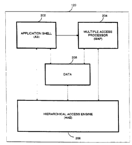
Figure 2 is a more detailed illustration of the hierarchical device extractor
module
120. The hierarchical device extractor module 120 comprises an application
shell module
(AS) 202, a multiple access processor module (MAP) 204, a hierarchical access
engine
module (HAE) 206, and a data module 208. The AS 202 uses rules data and design
data,
described below, to locate a device in the design data. The MAP 204 identifies
elements of
the device within a cell. The HAE 206 traverses the hierarchy of cells, from
the parent cell to
the associated leaf cell to identify interactions between device elements. The
AS 202, MAP
204, HAE 206, and data module 208 are described in greater detail below with
reference to
Figures 3-10.
* Trademark
-3c-
CA 02209305 2000-09-08
Figure 3 is a more detailed illustration of the HAE 206 of the preferred
embodiment.
The HAE 206 comprises a data-to-data processor module (DDP) 302, a cell-to-
data processor
module (CDP) 304, and a cell-to-cell processor module (CCP) 306. The DDP 302
identifies
the interaction between two elements that are located directly in a parent
cell, i.e., not lower
in the hierarchy. The CDP 304 identifies the interaction between two elements
of a device
where one element is located in the parent cell and one element is located in
a child cell, i.e.,
lower in the hierarchy. The CCP 306 identifies the interaction between two
elements of a
device where both elements are located at a level that is lower in the
hierarchy than the parent
cell. The DDP 302, the CDP 304, and the CCP 306 are discussed in greater
detail below.
Device extraction is the process of identifying a device (e.g., an NPN
transistor),
within an engineering design, e.g., an integrated circuit (IC) design. A
device is a
combination of one or more primitive components, e.g., an NPN transistor. As
described
above, a cell is a symbolic representation of primitive
-3 d-
CA 02209305 1997-07-02
WO 96/21902 PCT/US96/00342
the device are identified in a cell or the children cells of the cell and a
proper
relationship between the components is determined. The components of the
identified device are masked so that they are not identified and associated
with
another device during subsequent searches.
Figure 1 is an illustration of a computer according to a preferred embodiment.
The computer system 100 includes an input device 104 coupled to a central
processing unit (CPU) 108, the CPU 108 is also coupled to a display monitor
106, a
printer 110, a mass storage device 112 and random access memory (RAM) 116.
During computer operation the RAM 116 includes an operating system 118 and a
hierarchical device extractor 120. The input device 104, CPU 108, display 106,
printer
110, and mass storage 112 are all part of a conventional computing system,
e.g., a
SPARC Station 20 (commercially available from Sun Microsystem, Inc., Mountain
View, CA). In some embodiments the computer system is coupled to a network
114.
The RAM 116 includes an operating system 118, e.g., UNIX, and also includes a
hierarchical device extractor (HDE) program 120 that is described in detail
below.
Figure 2 is a more detailed illustration of the hierarchical device extractor
module 120. The hierarchical device extractor module 120 comprises an
application
shell module (AS) 202, a multiple access processor module (MAP) 204, a
hierarchical
access engine module (HAE) 206, and a data module 208. The AS 202 uses rules
data
and design data, described below, to locate a device in the design data. The
MAP 204
identifies elements of the device within a cell. The HAE 206 traverses the
hierarchy
of cells, from the parent cell to the associated leaf cell to identify
interactions between
device elements. The AS 202, MAP 204, HAE 206, and data module 208 are
described
in greater detail below with reference to Figures 3-10.
Figure 3 is a more detailed illustration of the HAE 206 of the preferred
embodiment. The HAE 206 comprises a data-to-data processor module (DDP) 302, a
cell-to-data processor module (CDP) 304, and a cell-to-cell processor module
(CCP)
306. The DDP 302 identifies the interaction between two elements that are
located
directly in a parent cell, i.e., not lower in the hierarchy. The CDP 304
identifies the
interaction between two elements of a device where one element is located in
the
parent cell and one element is located in a child cell, i.e., lower in the
hierarchy. The
CCP 306 identifies the interaction between two elements of a device where both
elements are located at a level that is lower in the hierarchy than the parent
cell. The
DDP 302, the CDP 304, and the CCP 306 are discussed in greater detail below.
Device extraction is the process of identifying a device (e.g., an NPN
transistor), within an engineering design, e.g., an integrated circuit (IC)
design. A
device is a combination of one or more primitive components, e.g., an NPN
transistor. As described above, a cell is a symbolic representation of
primitive
-4-
CA 02209305 1997-07-02
WO 96/21902 PCT/US96100342
components, e.g., wires and transistors. Each primitive componelt is located
on one
or more layers, e.g., a metal layer. The layers are created during the
fabrication
process. One layer can include many primitive components taking the form of
various geometries (shapes) on the layer. In addition, one layer can be a part
of
many cells and one cell can include many layers. The primitive components are
represented symbolically as shape data. Shape data of interest to device
extraction is
of two varieties, recognition shape data (RS) and terminal shape data (TS). A
device
is represented as a combination of one RS interacting with one or more TS's in
a
specific manner. The identity of the RS, the TS, and their required
interaction is
stored in the data module 208. The required interaction between shapes is
defined
by a rule. An example of a rule that defines an NMOS device having one
recognition
shape and three terminal shapes is given below.
device(NMOS)
recognitionShapeOn(NGATE)
terminalsOn(POLY, NSD, NSD);
The preferred embodiment searches the cell hierarchy for device components
and determines whether a combination of device components satisfy a rule
pertaining to a device.
The operating procedure or method of the hierarchical device extractor
module 120 is described with reference to Figures 4-10. Figure 4 is a symbolic
representation of a device in an integrated circuit design. The device
comprises the
RS 402 and two TS's 404, 406. The cells are represented by the letters T, A,
B, and C.
Cell C is a leaf cell and includes the RS 402. Cell B is a leaf cell and
includes TS 406.
Cell A is the parent cell of cell C and includes TS 404. Cell T is the parent
cell of cells
A and B. A device comprises RS 402, TS 404, and TS 406 interacting in the
manner
shown in Figure 4.
Figures 5A-5C are flowcharts showing the method of the application shell
module (AS) 202. The AS 202 receives 502 rules data (rules) and design data
from the
data module 208. As stated above, the rules define the device in terms of
shape data,
i.e., RS and TS, and the physical relationship between the shape data. The
design
data is the integrated circuit design data. The design data includes cell
data, shape
data, and masking data. The AS 202 groups 504 the rules such that rules
requiring
the same RS are grouped together. For example, all rules requiring a shape on
the
same layer are grouped together. Such a grouping technique can increase the
efficiency of the device extraction process. The AS 202 selects 506 a IZS, a
rule 508
from the selected RS group, and a leaf cell 510. During subsequent iterations,
the AS
202 selects a cell whose children cells have previously been selected and
processed.
Children cells include cells that are children cells of children cells, e.g.,
cell C is a
-5-
CA 02209305 1997-07-02
WO 96121902 PCT/US96/00342
child cell of cell T. In the example illustrated in Figure 4, the AS 202
selects 510 cell C,
although cell B could also have been selected.. The AS 202 invokes the HAE 206
to
identify and merge 514 the recognition shapes located within the selected
cell. The
HAE -206 identifies RS 402 within cell C. The technique for identifying a
shape using
the HAE 206 is described below. In this example the HAE 206 does not merge any
RS's because the entire RS is a single shape located within one cell, i.e.,
cell C. If the
RS were located in two or more cells the HAE 206 would combine, e.g., merge,
the RS
into one shape.
The AS 202 receives 518 masking data corresponding to RS's that have been
previously associated with a device. Once masked, an RS cannot be used to
identify
another device. The AS 202 invokes the MAP 204 to retrieve 520 shape data sets
that
are candidates for devices.
Figure 6 is a flowchart showing the method of the MAP. The MAP receives
602 design data from the data module 208. The MAP 204 uses the HAE 206 to
identify 604 all RS's that are located in the selected cell, i.e., cell C, and
all cells lower
in the hierarchy than the selected cell. The method used by the HAE 206 is set
forth
below. Although there is only one RS for each device, there may be multiple
RS's
within a cell because one cell can contain multiple devices. If multiple
children cells
of the selected cell contained a portion of the RS, the MAP 204 combines the
RS
portions to identify 604 one contiguous RS. The MAP 204 then removes 606 any
duplication from the RS's. RS duplication can occur when two cells overlap and
contain the same RS. The MAP 204 selects 610 a RS and invokes the HAE 206 to
identify 614 all TS's that interact, e.g., overlap or abut, with the selected
RS.
Figure 7 is a flowchart showing the technique for determining shape
interaction according to the HAE 206. The HAE 206 receives 702 cell data from
the
data module 208, e.g., the RS and the TS to be compared. When identifying
interactions between the RS and the TS, the HAE 206 determines the location of
the
two components (shapes), i.e., RS and TS, using design data located in the
storage
module 208, described below. If both shapes exist in the selected, i.e.,
parent, cell 704,
the HAE 206 invokes 706 the DDP 302. If only one shape is in the selected cell
708,
711, the HAE 206 invokes 710, 712 the CDP 304. If both shapes are in sub-cells
714,
i.e., children cells, the HAE 206 invokes 716 the CCP 306. In the example,
cell C was
selected. Although the RS is located within cell C, no TS's are located in
cell C.
Therefore, the HAE cannot identify any interactions between the RS and a TS.
The MAP repeats steps 610 and 614 until all RS's in the cell are selected 608.
In
the example, only one RS is located in cell C, therefore, the MAP returns
functional
control (control) 616 to the AS. After selecting 510 and processing 514-528
cell C, the
AS 202 compares the retrieved shaped data from the HAE 306 and determines 524
if
-6-
CA 02209305 1997-07-02
WO 96/21902 PCT/US96100342
the retrieved shape data satisfies the device definition. After processing
cell C,
neither of the necessary TS's are identified. Therefore, the device definition
is not
satisfied and the AS 202 selects 510 a new cell from the lowest available
level and
repeats steps 510-530.
The AS 202 selects 510 cell B. A TS 406 is located within cell B. However, the
RS 402 is located in cell A, which is not a child cell of cell B. Therefore,
when
processing cell B, the TS 406 and the RS 402 do not interact. The AS 202
determines
524 that the device definition is not satisfied because the rule is not
satisfied. The AS
202 then selects 510 a new cell whose children have all been previously
selected and
repeats steps 514-530.
The AS 202 selects 510 cell A. The RS 402 is wholly contained within cell C.
Therefore, the AS 202 does not need to merge 514 the RS, as described above.
The AS
202 receives 518 RS masking data. The RS 402 is available for device
identification
because the RS 402 is not masked. The AS 202 invokes the MAP 204 to retrieve
520
shape data sets from the design data that are candidates for devices. The MAP
204
receives data from the data module 208 and invokes the HAE 206 to identify 602
the
RS and all TS's that are fully contained within cell A and its children cells,
e.g., cell C.
TS 404 is identified by the HAE 206 for the MAP 204. After performing the
functions
defined in steps 604-610, discussed above, the MAP invokes the HAE 206 to
determine if TS 404 and RS 402 interact. The HAE 206 accomplishes this by
determining 708 that the TS 404 is located in the currently selected cell,
i.e., cell A,
and the RS 402 is located in a sub-cell of cell A, i.e., cell C. Therefore,
the HAE 206
invokes 710 the CDP 304 to determine if RS 402 and TS 404 interact.
Figure 9 is a flowchart showing the method of operation of the CDP 304. The
CDP 304 receives 901 a set of input cells and a set of input shapes. The CDP
304 then
selects 902 an input cell. The CDP 304 selects cell C because it is the only
child cell of
cell A. The CDP 304 determines 903 that the RS 402 does not exist in a child
cell of
cell C. The CDP 304 determines 905 that the RS 402 is located within cell C
and
invokes 906 the DDP 302 to determine if the RS 402 and the TS 404 interact.
Figure 8 is a flowchart showing the method of operation of the DDP 302. The
DDP 302 receives two sets of ordered shapes, one set having RS's and the other
set
having TS's. The shapes can be ordered using any of a variety of techniques,
for
example physical ordering, geographical ordering, fixed grid ordering,
variable grid
ordering, K-tree ordering, or quad-tree ordering. The DDP 302 selects 802 a
shape
from the first set of shapes SD1. In this example, the first set represents
RS's.
Alternatively, the first set can represent TS's. The DDP 302 selects 804 a
shape, e.g.,
TS 404, from the second set, SD2. The DDP 302 then determines 806 whether the
two
selected shapes interact. Any technique for determining if two shapes interact
can be
_7_
CA 02209305 1997-07-02
WO 96/21902 PCT/US96/00342
used. As an example, if a device rule defines an interaction to be any overlap
or
abutting of two shapes, and the two shapes were both geometrically
rectangular, the
DDP 302 calculates the sides of each shape and compares the sides to determine
if
they meet or overlap. In the example, the DDP 302 determines 806 that RS 402
and
TS 404 interact. Therefore, the DDP 302 stores 808 the shapes, i.e., RS 402
and TS 404,
for subsequent retrieval by the AS 202. The DDP 302 iterates 810 through each
shape
in the second set and then iterates 814 through each shape in the first set
before
returning 816 to the CDP 304.
The CDP 304 returns 908 control to the HAE 206. The HAE 206 returns 718
control to the MAP 202. The MAP 202 returns 616 control to the AS 202 after
determining 608 that all RS's have been selected. The AS 202 determines 524
that the
identified shape data set stored in the data module 208 by the DDP 302 does
not
satisfy the device definition because only one TS 404 interacts with the RS
402. The
AS 202 selects 510 a new cell from the lowest available level and repeats
steps 514-
530.
The AS 202 selects 510 cell T after selecting all cells lower in the
hierarchy. The
AS 202 invokes 520 the MAP 204 to identify all data sets, i.e., RS-TS
combinations,
that are candidates for devices. The MAP 204 receives 602 the shape data from
the
data module 208 and, using the HAE 206, determines that the RS 402 is in cell
C, the
TS 404 is in cell A, and the TS 406 is in cell B. The MAP 204 selects 610 the
RS 402 and
iteratively invokes 614 the HAE 206 to determine if the RS 402 and each of the
TS's
404, 406 interact. As described above, the HAE 206 receives 702, the RS 402
and a TS
406. The HAE 206 determines 714 that neither shape data are located in cell T,
i.e.,
they are both located in children cells of cell T. Therefore, the HAE invokes
716 the
CCP 306 to determine if RS 402 and TS 406 interact.
Figures 10A-10C are flowcharts showing the method of operation of the CCP
306. The CCP 306 receives 1002 two sets of cells, cell set 1 and cell set 2.
In the
example, cell set 1 includes cell A and cell set 2 includes cell B. The CCP
306 selects
1004 a child cell (CC) from the cell set 1, e.g., cell A. The CCP 306
determines 1006
which cells from cell set 2 interact with the CC. Cell B is the only cell from
cell set 2
that interacts with cell A. Therefore, the CCP 306 selects 1008 cell B as an
interacting
child cell (ICC). The CCP determines 1020 that the TS 406, i.e., one shape in
the
second set of shapes SD2, is located in cell B, i.e., the ICC, and that the RS
402, i.e.,
one shape in the first set of shapes SD1, is located in a child cell of cell
A, i.e., the CC.
The CCP 306 invokes 1022 the CDP 304.
The CCP 302 would proceed differently if the design were different. For
example, if RS 402 existed in the CC and TS existed in ICC 1010 the CCP 306
would
invoke 1012 the DDP 302. If RS 402 existed in the ICC and TS existed in CC
1014 the
_g_
CA 02209305 1997-07-02
WO 96/21902 PCT/US96/00342
CCP 306 would invoke 1016 the DDP 302. If TS existed in a child cell of the CC
and
RS existed in the ICC 1024, the CCP 306 would invoke 1026 the CDP 304. If RS
existed in the CC and TS existed in a child cell of the ICC 1030, the CCP 306
would
invoke 1032 the CDP 304. If TS existed in the CC and RS existed in a child
cell of the
ICC 1034, the CCP 306 would invoke 1036 the CDP 304. If RS existed in a child
cell of
the CC and TS existed in a child cell of the ICC 1040, the CCP 306 would
recursively
invoke 1042 the CCP. If TS existed in a child cell of the CC and RS existed in
a child
cell of the ICC 1044, the CCP 306 would recursively invoke 1046 the CCP.
In the example, as stated above, the CCP 306 invokes 1022 the CDP. The CDP
304, whose method of operation is described above with reference to Figure 9,
receives 901 input cells and input shapes and selects 902 cell C. The CDP 304
determines 905 that the RS 402 is located in cell C and invokes 906 the DDP
302. The
DDP 302, using the above described technique, determines that the RS 402 and
the TS
406 interact. The DDP 302 stores 808 RS 402 and TS 406 and returns control 816
to
the CDP 304. The CDP 304 returns control 908 to the CCP 306. After all
interacting
child cells have been selected 1047 from cell set 2 and all children cells
have been
selected from cell set 1 1048, the CCP 306 returns control 1050 to the HAE
206. The
HAE 206 returns control 718 to the MAP 204. At this point the interaction
between
the RS 402 and the TS 406 has been identified and stored in the data module
208.
Next, the MAP 204 determines whether the RS 402 and the other TS 404
interact. As described above, the MAP 204 iteratively invokes 614 the HAE 206
to
determine if RS 402 and TS 404 interact. The HAE 206 receives 702 the current
cell
data that include the RS 402 and the TS 404. The HAE 206 determines 714 that
RS 402
and TS 404 are both located in children cells of cell T. Therefore, the HAE
206
invokes 716 the CCP 306. The CCP 306 receives two cell sets. Cell set 1
includes cell
A. Cell set 2 also includes cell A because cell C is a child of cell A. The
CCP 306
selects 1004 a CC, i.e., cell A, from cell set 1. The CCP 306 determines 1006
which cell
from cell set 2 interact with the CC. The CCP 306 determines 1006 that cell A
interacts with itself. The CCP 306 selects cell A to be the ICC. Therefore,
cell A is
both the CC and the ICC. The CCP 306 determines 1020 that RS 402 is located in
a
child cell of cell A and that the TS is located in cell A and invokes 1022 the
CDP 304.
The CDP 304 selects 902 cell C, determines 905 that the RS 402 is located in
cell
C, and invokes 906 the DDP 302. Using the technique described above, the DDP
302
determines 806 that the RS 402 and the TS 404 interact. The DDP 302 returns
control
816 to the CDP 304 that returns control 908 to the CCP 306. The CCP 306
returns
control 1050 to the HAE 206. Then the HAE 206 returns control 718 to the MAP
204
and the MAP 204 returns control 616 to the AS 202. The interaction between the
RS
402 and the TS 406 has been identified and stored in the data module.
-9-
CA 02209305 1997-07-02
WO 96121902
PCT/US96/00342
The AS 202 retrieves the stored data set and determines 524 that the shape
data set satisfies the device definition, described above. The AS 202 stores
526 the
shape data with the design data of the cell. The AS 202 masks 528 the RS 402
to
prevent the RS 402 from being identified and associated with another device.
After
determining 530 that the top cell has been selected, the AS 202 repeats steps
510-530
for each rule in the RS group. The AS 202 repeats steps 508-534 for each
recognition
shape in the IC design. After all recognition shapes have been processed 536
the AS
202 determines 538 if any recognition shapes have not been masked and
generates
540 an error message if one or more recognition shapes are unmasked.
The hierarchical device extractor 120 identifies device components that are
located within one or more cells even if the cells are hierarchical in
relation to each
other. The hierarchical device extractor 120 permits a IC designer to develop
more
complex designs and more efficient designs by removing the limitation that all
components must exist within one cell.
-10-