Note: Descriptions are shown in the official language in which they were submitted.
CA 02209425 1997-07-04
SOLENOID DRIVER CIRCUIT
Background of the Invention
This invention relates to an electrical circuit for providing controlled
electrical current
to a solenoid, such as the solenoid of a hydraulic control valve.
It is desired to use analog current controlled solenoid valves to control the
hydraulic
pressure applied to clutches in a power-shift transmission. Precise current
control is
required for smooth and predictable modulation of the transmission elements
when shifting
from one gear to another. Because of power dissipation, it is not practical on
a vehicle to
control current to an analog valve by controlling the voltage supply to it.
So, to generate the
desired current command, the supply voltage is pulsed on and off at a fast
rate. The
inductance in the coil stores energy when the voltage is pulsed on, and
releases energy
when the voltage is off, thus producing an average current.
However, current control is difficult in such an application because the
primary
electrical characteristics of the control valves, resistance and inductance,
are unknown and
unpredictable. Resistance of the coil can change by over 100°/a
throughout the temperature
range to which it is subjected. Similarly, the inductance of the coil can
change by well over
100% due to variations of temperature, voltage pulse frequency, and supply
current.
Furthermore, the amplitude of the voltage pulses can range from 9 to 16 volts.
It is known to filter the pulsing current, measure its average, and compensate
the
command until the desired average current is achieved. But, such a technique
does not
work well in a transmission control application. This because during a shift
the command to
a valve is changing rapidly. The command is either ramping up or down
depending on
whether the transmission element is coming on or going off. To measure real-
time average
current the command must be held constant for some time. But, during a shift
there is not
sufficient time available for this to be done. Therefore, it would be
desirable to have a valve
driver which produces an accurate average current in a coil that has an
unknown resistance
and an unknown inductance without feedback sensing of the average current.
Summary of the Invention
An object of the present invention is to provide a solenoid valve driver which
produces an average current which is linearly related to commanded peak
current.
Another object of the present invention is to provide a valve driver wherein
the coil
current will have a lower peak current value which is substantially a fixed
percentage of the
upper peak current value.
Another object of the present invention is to provide precise current control
of a
solenoid driver with immediate response (minimum delay between commanded
current and
actual current).
CA 02209425 1997-07-04
Another object of the present invention is to provide a system for controlling
solenoid
current which can be made with few components and at low cost, and which
places few
demands (software overhead) on a microprocessor.
Another object of the present invention is to optimize the frequency of the
solenoid
driver at the nominal operating point (nominal current, resistance, inductance
and supply
voltage) by selecting the proper resistor divider network.
Another object of the present invention is to provide the maximum fault
detection of
the solenoid driver circuit.
Another object of the present invention is to provide a circuit wherein the
output
current to the solenoid is zero on power-up and/or during the reset mode of
the
microprocessor.
These and other objects are achieved by the present invention wherein an
electrical
circuit applies an oscillatory electrical current to a coil of a solenoid in
order to cause the
solenoid to move in response to a command signal. The circuit includes a
signal divider for
generating an upper peak current signal value from the command signal and a
lower peak
current signal value which is a fixed percentage of the upper peak current
signal value. A
current sense resistor generates a current sense voltage representing current
through the
coil. A first comparator compares the current sense voltage to the upper
current signal
value. A second comparator compares the current sense voltage to the lower
current signal
value. A current driver applies a driving current to the solenoid coil as a
function of output
signals generated by the first and second comparators so that the coil current
will have a
lower peak current value which is substantially a fixed percentage of the
upper peak current
value. The average current linearly follows the peak current because the lower
peak is
always a fixed percentage of the commanded upper peak current. As the ratio
between
peaks is constant, the linearity between average current and commanded peak
current
holds even if the inductance and/or resistance of the coil changes or if the
supply voltage
changes. As peak-to-peak amplitude increases with the average current, the
frequency
range of the solenoid driver is minimized.
Brief Description of the Drawings
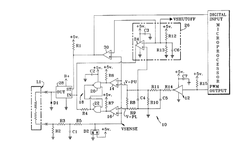
The sole Figure is a detailed circuit diagram of the solenoid driver circuit
of the
present invention.
2
CA 02209425 1997-07-04
Detailed Description
The solenoid driving circuit 10 controls the current applied to the coil L1 of
a solenoid
operated transmission control valve (not shown) in response to an analog
voltage command
signal V-CMD generated by the PWM output of a microprocessor MP. Preferably,
the
command signal will have a voltage range of 0 to 5 volts corresponding to a
desired coil
current of 0 to 1000 miliamps. Pull-up resistor R15 (connected to a 5 volt
regulator supply
voltage) and inverter 12 convert the commanded PWM signal of 0% to 100% duty
cycle to 5
to 0 volts analog voltage using a 2 milisecond filter circuit comprised of
resistor R14 and
capacitor C5.
The filtered command signal is then applied to a voltage divider formed by
resistors
R11 and R10 which supplies a commanded voltage V-PU (voltage peak-upper) at
the
common connection therebetween. A slight amount of additional filtering is
supplied by
capacitor C4 which is connected in parallel with R10. The voltage V-PU is
applied to the +
input of a reset command comparator 14 and to a voltage divider formed by
resistors R8
and R9 connected between V-PU and ground. The common connection between R8 and
R9 provides a V-PL (voltage peak-lower) signal which is a certain fixed
percentage of V-PU,
and which is applied to the - input of a set command comparator 16.
The output of reset command comparator 14 is connected to +5 volts via
resistor R6
and is applied to an input of a set/reset flip flop 18 (with Schmidt Trigger
input) formed by a
pair of cross-connected NAND gates 20, 22 and capacitor C2. The output of set
command
comparator 16 is connected to +5 volts via resistor R7 and is applied to the
an input of a
set/reset flipflop 18.
V-PU is also applied to the + input of comparator 24 which, with grounded
capacitor
C3, is part of a shutoff circuit 26. A voltage divider formed by resistor R12
and R13 between
+5 volts and ground generates a shutoff voltage V-SHUTOFF which is applied to
the - input
of comparator 24 so that comparator 24 will generate a shutoff signal until V-
PU reaches a
level representing a coil current of approximately 150 miliamps. A capacitor
C6 is
connected between ground and the common connection between R12 and R13. The
output
of comparator 24 (and of shutoff circuit 26) is connected to the IN input of
driver 28. The
output of driver 28 is connected to one end of the solenoid coil L1 and to
ground via fly-back
diode D1.
The other end of coil L1 is connected to ground via current sense resistor R2.
The
3
CA 02209425 1998-06-09
voltage across resistor R2 is proportional to the current through coil L1, and
is filtered from
high frequency noise by resistor R3, capacitor C1 and resistor R5 to generate
a voltage
VSENSE. Voltage transient suppression is performed by diode D2. Voltage VSENSE
is
applied to the + input of comparator 16 and to the - input of comparator 14.
A comparator 30 has a + input to which is applied VSENSE and a - input to
which is
applied voltage VSHUTOFF. The output of comparator 30 is connected to +5 volts
via pull-up
resistor R1 and to the status input ST of driver 28 and pulls the ST input low
when VSENSE is
below VSHUTOFF. The output of comparator 30 generates a status signal which is
applied to
a digital input of the microprocessor MP so that the microprocessor can detect
circuit faults
when the commanded voltage V-PU is greater than a value corresponding to a
coil current of
150 miliamps. The status signal must be ignored until the command is greater
than 150
miliamps.
Preferably, the driver 28 may be a Siemens' Profet device or equivalent, which
has
built-in features to detect open or short circuits in the coil L1. When the
driver 28 detects a
fault, it pulls its status line ST low.
Comparator 16 pulls its output to ground when VSENSE is too low (less than V-
PL).
Comparator 14 pulls its output to ground when VSENSE is too high (greater than
V-PU). In
this example, resistors R8 and R9 are chosen so that V-PL is 78.5% of V-PU.
When VSENSE
is below V-PL, the driver 28 is turned on (set) and remains on until VSENSE
climbs above V-
PU. When VSENSE reaches V-PU, the driver 28 is turned off (reset) until once
again
VSENSE falls below V-PL.
To make sure the driver 28 is off when the commanded voltage is too low, the V-
PU
and a small fixed voltage VSHUTOFF are fed into the comparator 24. When the
commanded
voltage from the microprocessorMP is less than a value corresponding to a coil
current of 150
miliamps the comparator 24 pulls the input to driver 28 low, turns the driver
28 off, and
prevents flip-flop 18 from turning the driver 28 on.
With this circuit, the average current through coil L1 linearly follows the
peak current
because the lower peak current is always a fixed percentage of the upper peak
current. As
the command increases the peak-to-peak amplitude increases, but the ratio
between the
upper peak and the lower peak is constant. The linearity holds even if the
inductance and/or
resistance of the coil changes and/or if the supply voltage changes.
Thus, as the command signal varies, the coil current upper peak and lower peak
values vary while the variable coil current lower peak value remains a fixed
percentage of the
4
CA 02209425 1998-06-09
variable coil current upper peak value.
This circuit will run at a variable frequency. The frequency varies as a
function of
command voltage, resistance and inductance of a coil, and supply voltage. But
since peak-to-
peak amplitude increases as the average current increases, the frequency
variation is much
less than if the peak-to-peak amplitude was constant. The R8, R9 resistor
divider ratio can be
chosen to optimize the frequency at the nominal operating point (nominal
current, resistance
and inductance of a coil, and supply voltage).
One of these control circuits can be used with multiple drivers if the drivers
are never
on at the same time. For example, one forward and one reverse driver could
share a common
low-side return and current sense circuit. The input to the forward driver
could simply be
ANDed with the forward switch, and the reverse driver ANDed with the reverse
switch. The
microprocessorwould drive the same command circuit regardless of which valve
was actually
being supplied.
Finally, this circuit is simple and consists of inexpensive components.
Microprocessor
overhead is extremely light as it only has to generate the PWM command signal.
A/D inputs
are not tied up since average current is not measured by the microprocessor.
No equations or
tables are required to convert duty cycle to current since the relationship is
linear. However,
the PWM signal should have a fairly high frequency so the time constant of
R14, C5 filter can
be minimized, or D/A converters could be used as well. Note that the sense
resistor R2
should be chosen as large as possible and should preferably have a ~~ 1 %
tolerance.
Likewise, resistors R8, R9, R10, R11 and R14 should preferably have a ~~ 1 %
tolerance. The
ground path between the sense resistor R2 and the comparators 14, 16, 24 and
30 should
have a very low impedance. The accuracy of the 5 volt regulator supply voltage
supplied to
the inverter 12 is also important.
The following is a table of components which may be used in the electronic
circuits
illustrated in the Figure. These components are merely exemplary and other
components
could be utilized without departing from scope of the present invention.
CA 02209425 1997-07-04
Exemplary Components
Resistors
R1, R6, R7, R15 10 kOhms
R2 1.0 Ohms
R3, R5 4.7 k
R4 2.7 k
R8 13 k
R9 47.5 k
R10 10.2 k
R11 23.7 k
R12 27.4 k
R13 1.0 k
R14 6.04 k
Capacitors
C 1 47 pf
C2, C3, C4, C6, C7 .047 Mf
C5 .33 Mf
Diodes
D1 GI S2G
D2 BAV99
Integrated Circuits
12 74HC14 (Hex schmidt trigger Inverter)
14, 16, 24, 30 LM2901 (Quad comparator)
20, 22 74HC08 (Quad schmidt trigger Nand gates)
28 BTS410F
Microprocessor 8 Bit (80C517A)
While the invention has been described in conjunction with a specific
embodiment, it
is to be understood that many alternatives, modifications and variations will
be apparent to
those skilled in the art in light of the foregoing description. For example,
without departing
6
CA 02209425 1997-07-04
from the principle of the invention, the non-inverting power switching device
could be
replaced with an inverting device with an inverting intermediate driver stage.
Accordingly,
this invention is intended to embrace all such alternatives, modifications and
variations
which fall within the spirit and scope of the appended claims.
7