Note: Descriptions are shown in the official language in which they were submitted.
CA 02209620 1997-07-07
SEMICONDUCTOR DEVICE
BACKGROUND OF THE INVENTION
Field of the Invention:
This invention relates to a semiconductor device, and
particularly to a semiconductor device suitable for use in
a power FET that handles a high-frequency signal.
Description of the Related Art:
As a technique related to this type of FET, one
described in the following reference, for example, has
heretofore been known.
Reference: John L.B. Valker, rHigh Power GaAs FET
AmplifierJ, ARTECH HOUSE, INC., P.123, 1993.
Fig. 3 is a pattern plan view showing an example of
one configuration of a conventional power FET described in
the above-described reference.
This type of FET comprises a region l activated as the
FET, a row 2 of pads used to draw drain terminals, and a
row 3 of pads used to draw gate and source terminals.
The pads for the drains are arranged at uniform
intervals as shown in the drawing. Further, the pads for
the gates and sources are also alternately placed at
uniform intervals.
The conventional power FET has a drawback in that it
oscillates at a frequency dependent on the size of the
interval between the pads upon its operation.
CA 02209620 1997-07-07
This drawback will be explained below. In the
conventional power FET, the drain pads used as the same
terminals exist in plural form as shown in Fig. 3.
This is because there is a restriction on the amount
of power capable of being taken out of one pad. In order
to set power quantities capable of being taken out of the
respective pads as uniform as possible or for convenience
of the formation of patterns, the intervals between the
adjacent pads have heretofore been rendered uniform as
shown in Fig. 3 in consideration of workability or the like
at wire-bonding. The same signals, i.e., signals identical
in amplitude and phase to each other are supplied to the
plurality of pads for the drains. However, since the
intervals between the pads are uniform, standing waves in
which the positions of the pads are set as nodes, can
exist.
Thus, oscillations are apt to take place at a
frequency at which the interval between the pads is set to
one or half wavelength. The oscillations are apt to occur
even in the case of the pad row of the sources and gates.
As has been described above, the conventional power
FET has a drawback in that the oscillations take place at
the frequency at which the interval between the pads is set
to one or half wavelength.
SUMMARY OF THE INVENTION
With the forgoing in view, it is therefore an object
of the present invention to provide a power FET hard to
CA 02209620 1997-07-07
generate oscillations at a frequency dependent on the
interval between adjacent pads.
According to one aspect of the present invention, for
achieving the above object, there is provided a
semiconductor device including:
a power FET which comprises a plurality of pads used
for drawing gate, source and drain terminals and wherein a
row of the drain pads is disposed on one side of a chip and
a row of the gate and drain pads is disposed on the side
opposite to the one side thereof; and
wherein the intervals between the pads in the pad row
of the drains employed in the power FET are set to unequal
intervals.
According to another aspect of the present invention,
for achieving the above object, there is provided a
semiconductor device including:
a power FET which comprises a plurality of pads used
for drawing gate, source and drain terminals and wherein a
row of the drain pads is disposed on one side of a chip and
a row of the gate and drain pads is disposed on the side
opposite to the one side thereof; and
wherein the intervals between the pads in the pad row
of the drains and gates employed in the power FET are set
to unequal intervals.
Typical ones of various inventions of the present
application have been shown in brief. However, the various
inventions of the present application and specific
configurations of these inventions will be understood from
the following description.
CA 02209620 1997-07-07
BRIEF DESCRIPTION OF THE DRAWINGS
While the specification conciudes with claims
particularly pointing out and distinctly claiming the
subject matter which is regarded as the invention, it is
believed that the invention, the objects and features of
the invention and further objects, features and advantages
thereof will be better understood from the following
description taken in connection with the accompanying
drawings in which:
Fig. 1 is a pattern plan view of a power FET employed
in a semiconductor device showing a first embodiment of the
present invention;
Fig. 2 is a pattern plan view of a power FET employed
in a semiconductor device illustrating a second embodiment
of the present invention; and
Fig. 3 is a pattern plan view of a power FET employed
in a conventional semiconductor device.
DETAILED DESCRIPTION OF THE PREFERRED EMBODIMENTS
Semiconductor devices of the present invention will
hereinafter be described by preferred embodiments with
reference to the accompanying drawings. Figs. 1 and 2
simply schematically show the relationship between shapes,
dimensions and positions to the extent that the present
irvention can be understood.
[First embodiment]
CA 02209620 1997-07-07
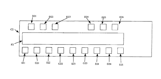
Fig. 1 a plan view of a chip for a power FET showing a
first embodiment of a semiconductor device according to the
present invention.
As shown in Fig. 1, a pad row of drains has six pads
in the same manner as that employed in the prior art shown
in Fig. 3. The amount of power per pad is identical to
that employed in the prior art shown in Fig. 3. However,
the pads are arranged side by side at equal intervals in
the conventional power FET, whereas in the present
invention, the interval between pads D23 and D24 is wider
than that between adjacent other pads and hence the pads
are arranged at une~ual intervals.
When a standing wave attempts to occur or develop at a
wavelength corresponding to the interval between pads D21
and D22 in the case of the pad layout or arrangement shown
in Fig. 1, a wavelength corresponding to the interval
between the pads D23 and D24 differs from that wavelength.
Thus, no standing wave is produced. When the standing wave
attempts to occur at a wavelength corresponding to the
20 interval between the pads D23 and D24, wavelengths
corresponding to the interval between the pads D22 and D23
and the interval between the pads D24 and D25 differ from
the wavelength corresponding to the interval between the
pads D23 and D24. Thus, the standing wave eventually leads
to non-generation.
According to the first embodiment as described above,
since the intervals between the adjacent pads of the pad
row, which are used for the drawing drain terminals, are
rendered nonuniform, the standing wave attributed to the
CA 02209620 1997-07-07
pad-to-pad interval is not produced. Thus, a power FET can
be provided which is hard to oscillate at a frequency
dependent on the pad-to-pad interval.
[Second embodiment]
A second embodiment of a semiconductor device
according to the present invention will next be described
with reference to a plan view of a power FET shown in Fig.
2.
The second embodiment shown a case in which the
intervals between pads of a pad row composed of gates and
sources are held uneven. In a power FET, a large current
or high power is generally supplied to pads for drains and
sources, whereas a large current or power is not supplied
to pads for gates so far. Thus, in the second embodiment,
the number of the pads for the sources is set to the same
as that employed in the conventional power EET and the
number of the pads for the gates is reduced.
When a standing wave attempts to develop at a
wavelength corresponding to the interval between pads G31
and S32 in a pad layout shown in Fig. 2, a wavelength
corresponding to the interval between pads S32 and S33
differs from that wavelength. Therefore, the standing wave
is not produced eventually. On the other hand, when a
standing wave attempts to occur at a wavelength
corresponding to the interval between the pads S32 and S33,
the wavelength corresponding to the interval between the
pads G31 and S32 and a wavelength corresponding to the
interval between the pads S33 and S34 differ from the
wavelength corresponding to the interval between the pads
- 6 -
CA 02209620 1997-07-07
S32 and S33. Thus, the standing wave eventually leads to
non-generation.
Further, the gates are used as inputs of the present
power FET. Thus, when oscillations are generated on the
gate side, the oscillations are amplified by the FET so as
to appear on the drain side when the frequency of the
oscillations falls within an operation frequency range of
the FET. Accordingly, the prevention of the oscillations
on the gate side or input side is of importance.
According to the second embodiment of the present
invention as described above, since the intervals between
the pads of the pad row, which are used for the drawing of
gate and source terminals, are rendered uneven, the
standing wave attributable to the pad-to-pad interval is
not produced. Thus, a power FET can be provided which is
hard to oscillate at a frequency dependent on the interval
between the pads.
According to the semiconductor devices of the present
invention, as has been described above in detail, the first
embodiment can bring about an advantageous effect in that
the oscillations attributed to the interval between the
adjacent pads on the drain side of the power FET can be
prevented.
Further, the second embodiment of the present
invention can bring about an advantageous effect in that
the oscillations attributed to the interval between the
adjacent pads on the gate and source sides of the power FET
can be prevented.
CA 02209620 1997-07-07
Moreover, the first and second embodiments of the
present invention can be simultaneously carried out. In
this case, the oscillations caused by the interval between
the adjacent pads can be prevented on both sides of the
drain side and the gate and source sides.
In the illustrated embodiments, the row of the pads
for the source terminals and the row of the pads for the
gate terminals have been placed on the same side. However,
the pads for the gate terminals may be placed on the other
side.
While the present invention has been described with
reference to the illustrative embodiments, this description
is not intended to be construed in a limiting sense.
Various modifications of the illustrative embodiments, as
well as other embodiments of the invention, will be
apparent to those skilled in the art on reference to this
description. It is therefore contemplated that the
appended claims will cover any such modifications or
embodiments as fall within the true scope of the invention.