Some of the information on this Web page has been provided by external sources. The Government of Canada is not responsible for the accuracy, reliability or currency of the information supplied by external sources. Users wishing to rely upon this information should consult directly with the source of the information. Content provided by external sources is not subject to official languages, privacy and accessibility requirements.
Any discrepancies in the text and image of the Claims and Abstract are due to differing posting times. Text of the Claims and Abstract are posted:
| (12) Patent Application: | (11) CA 2210222 |
|---|---|
| (54) English Title: | A METHOD OF PRODUCING AN OHMIC CONTACT AND A SEMICONDUCTOR DEVICE PROVIDED WITH SUCH OHMIC CONTACT |
| (54) French Title: | PROCEDE DE FABRICATION D'UN CONTACT OHMIQUE ET DISPOSITIF A SEMI-CONDUCTEUR EQUIPE D'UN TEL CONTACT OHMIQUE |
| Status: | Dead |
| (51) International Patent Classification (IPC): |
|
|---|---|
| (72) Inventors : |
|
| (73) Owners : |
|
| (71) Applicants : |
|
| (74) Agent: | ERICSSON CANADA PATENT GROUP |
| (74) Associate agent: | |
| (45) Issued: | |
| (86) PCT Filing Date: | 1996-01-17 |
| (87) Open to Public Inspection: | 1996-07-25 |
| Examination requested: | 2003-01-10 |
| Availability of licence: | N/A |
| (25) Language of filing: | English |
| Patent Cooperation Treaty (PCT): | Yes |
|---|---|
| (86) PCT Filing Number: | PCT/SE1996/000035 |
| (87) International Publication Number: | WO1996/022611 |
| (85) National Entry: | 1997-07-11 |
| (30) Application Priority Data: | ||||||
|---|---|---|---|---|---|---|
|
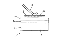
In a method of producing an ohmic contact (5) to a p-type .alpha.-SiC layer (3b) in a semiconductor device (1), layers of aluminium, titanium and silicon are deposited on said .alpha.-SiC layer (3b), and said deposited layers (5) are annealed to convert at least part of said deposited layers (5) to aluminium-titanium-silicide.
Cette invention concerne un procédé de fabrication d'un contact ohmique (5) pour une couche .alpha.-SiC de type p (3b) dans un dispositif à semi-conducteur (1). Des couches d'aluminium, de titane et de silicium sont déposées sur ladite couche .alpha.-SiC (3b). Les couches déposées (5) sont ensuite soumises à un recuit afin qu'elles (5) soient, au moins en partie, converties en siliciure d'aluminium et de titane.
Note: Claims are shown in the official language in which they were submitted.
Note: Descriptions are shown in the official language in which they were submitted.
Sorry, the description for patent document number 2210222 was not found. Text is not available for all patent documents. The current dates of coverage are on the Currency of Information page
For a clearer understanding of the status of the application/patent presented on this page, the site Disclaimer , as well as the definitions for Patent , Administrative Status , Maintenance Fee and Payment History should be consulted.
| Title | Date |
|---|---|
| Forecasted Issue Date | Unavailable |
| (86) PCT Filing Date | 1996-01-17 |
| (87) PCT Publication Date | 1996-07-25 |
| (85) National Entry | 1997-07-11 |
| Examination Requested | 2003-01-10 |
| Dead Application | 2006-02-23 |
| Abandonment Date | Reason | Reinstatement Date |
|---|---|---|
| 2005-02-23 | R30(2) - Failure to Respond | |
| 2006-01-17 | FAILURE TO PAY APPLICATION MAINTENANCE FEE |
| Fee Type | Anniversary Year | Due Date | Amount Paid | Paid Date |
|---|---|---|---|---|
| Registration of a document - section 124 | $100.00 | 1997-07-11 | ||
| Application Fee | $300.00 | 1997-07-11 | ||
| Maintenance Fee - Application - New Act | 2 | 1998-01-20 | $100.00 | 1998-01-13 |
| Maintenance Fee - Application - New Act | 3 | 1999-01-18 | $100.00 | 1999-01-07 |
| Maintenance Fee - Application - New Act | 4 | 2000-01-17 | $100.00 | 2000-01-11 |
| Maintenance Fee - Application - New Act | 5 | 2001-01-17 | $150.00 | 2001-01-08 |
| Maintenance Fee - Application - New Act | 6 | 2002-01-17 | $150.00 | 2002-01-15 |
| Request for Examination | $400.00 | 2003-01-10 | ||
| Maintenance Fee - Application - New Act | 7 | 2003-01-17 | $150.00 | 2003-01-13 |
| Maintenance Fee - Application - New Act | 8 | 2004-01-19 | $150.00 | 2003-12-08 |
| Maintenance Fee - Application - New Act | 9 | 2005-01-17 | $200.00 | 2004-12-21 |
Note: Records showing the ownership history in alphabetical order.
| Current Owners on Record |
|---|
| TELEFONAKTIEBOLAGET LM ERICSSON |
| Past Owners on Record |
|---|
| KRONLUND, BERTIL KARL |

