Note: Descriptions are shown in the official language in which they were submitted.
CA 022l0~36 Iss7-07-l~
WO96/22s62 PCT/GB96/00072
OPTICAL SWITCH
BACKGROUND TO THE INVENTION
~ The present invention relates to an optical switch
which might be used, for example, as a demultiplexer for
adding or dropping OTDM (optical time-division
multiplexing) channels in an optical telecommunications
system.
It has been recognised that in order to achieve the
highest possible bit rates (e.g. of 100 Gbit/s or more) in
optical transmission systems it is desirable that functions
such as adding or dropping a channel should be carried out
entirely in the optical domain. It has previously been
proposed to carry out such functions using a non-linear
loop mirror (NOLM) in which the non-linearity is provided
by a semiconductor gain medium which is positioned
asymmetrically in the loop. Incoming optical data is split
into two counter-propagating components. Because the
semiconductor gain medium is positioned asymmetrically, one
of these components passes through it before the other.
Accordingly, if an optical control signal is applied to the
gain medium to switch it after the first component has
passed through but before the second counter-propagating
component has arrived, then the two components experience
different phase shifts through the semiconductor gain
medium, producing a differential phase shift which may used
to switch the signal to determine whether it is transmitted
or reflected by the NOLM.
Although, as described in the present applicant's co-
pending International application PCT/GB94/02240, it is
found to be possible to operate such an NOLM at switching
rates higher than the saturation recovery time of the
semiconductor optical gain medium, nonetheless there
remains a fundamental upper limit to the possible switching
speeds determined largely by the transit time associated
with the semiconductor gain medium. In use, there has to
be time for the first pulse to pass through the gain
medlum, then for the gating pulse to pass through, and
CA 02210~36 1997-07-1~
WO 96/22S62 PCTl~;b~G/'~, 1)072
subsequently for the second pulse to pass through the
medium. This limits the possible bit-rate which can be
handled by the switch.
SUMMARY OF THE INVENTION
According to a first aspect of the present invention,
an optical switch comprising a semiconductor gain medium
and means for applying an optical control signal to the
semiconductor gain medium is characterised by a pair of
arms arranged in a Mach-Zehnder configuration with a
respective semiconductor gain medium connected in each arm,
in use respective control signals being applied to each
semiconductor gain medium with a delay between the control
signals selected so that a differential phase shift is
applied to an input optical signal propagating through the
arms of the switch, and by a phase control element
connected in one of the arms of the switch and arranged to
cancel a phase offset between pulses propagating in the two
arms.
The present invention provides an optical switch using
a semiconductor optical gain medium arranged in such a way
that the switching rate is not limited by the transit time
of the gain medium. To this end, a pair of semiconductor
gain elements are used in the two arms of a Mach-Zehnder
interferometer. By appropriate control of the period and
relative delay of a sequence of control pulses applied to
the respective gain media, a differential phase shift can
be applied to a selected one or more of the pulses in an
optically encoded data stream so that selected pulses are
output from a different port of the switch. The switching
rate is not limited by the transit time of the
semiconductor gain media and so higher rates can be
achieved than hitherto has been possible. Furthermore, the
switch achieves contrast/extinction ratios superior to
those of conventional NOLM switches when used at high bit-
rates.
As will be further described below, while the selectedone or more pulses experience a differential phase shift,
CA 022l0~36 lsg7-07-l~
W096l22562 PCT/Gb9CI00072
e.g. of ~, the other pulses experience a small differential
phase shift from the two semiconductor gain media
correlated to the delay between the two control sequences.
However, the present inventors have found that this
residual differential can be substantially entirely
cancelled by the provision of a simple phase-shifting
element in one of the arms of the Mach-Zehnder
interferometer.
Preferably the switch is a demultiplexer arranged to
select one or more pulses from an input optical pulse
stream.
The high switching rates and excellent contrast ratios
obtainable with the switch of the present invention make it
particularly valuable as an optical demultiplexer suitable
for use in optical telecommunication systems. The input
pulse stream might comprise, for example, a series of OTDM
frames with the demultiplexer being used to select a given
one or more channels from each OTDM frame for routing to a
different output port.
According to a second aspect of the present invention,
there is provided a method of switching an optical signal
to select one or more pulses from a pulse stream, the
method including applying the signal to a semiconductor
gain medium, and applying an optical control signal to the
semiconductor gain medium, characterised by splitting the
optical signal between a pair of arms arranged in a Mach-
Zehnder configuration and passing the signal in each arm
through a respective semiconductor gain medium, applying
respective optical control signals to each semiconductor
gain medium with a delay between the control signals
selected so that a differential phase shift is applied to
the signal, and applying a further phase shift to cancel a
phase offset between pulses propagating in the pair of
arms.
According to a third aspect of the present invention
an optical demultiplexer arranged to select one or more
pulses from an input optical pulse stream is characterised
CA 022l0~36 lss7-07-l~
W096/22S62 PCT/GB96/00072
by a switch in accordance with the first aspect of the
present invention arranged to switch the selected one or
more pulses in response to the said control signals.
Another important field of use for the optical switch
of the present invention is in signal processing and clock
recovery. The switch may advantageously be substituted for
the non-linear optical modulator (NOM) of a clock recovery
circuit such as those described and claimed in the present
applicant's published International application W093/22855
lo (PCT/GB93/00863).
The switch may also be used as a correlator for
sampling a repetitive optical signal. Used in this manner
it might form the basis of an "all-optical" oscilloscope
(that is to say an oscilloscope in which signal sampling is
carried out in the optical domain) or other test
instrument. In this case the control signals applied to
the semiconductors would take the form of a repetitive
periodic signal having a frequency close to but different
from the frequency of the signal to be sampled, differing,
for example, by a few kHz.
DESCRIPTION OF THE DRAWINGS
Embodiments of the present invention will now be
described in further detail, by way of example only, with
reference to the accompanying drawings in which:
Figure 1 is a schematic of a conventional NOLM;
Figure 2 is a graph showing the phase response of the
NOLM of Figure 1;
Figure 3 is a first example of a demultiplexer
embodying the present invention;
Figure 4 is a graph showing the phase response of the
demultiplexer of Figure 3;
Figure 5 is a timing diagram showing the data and
control pulses for the demultiplexer of Figure 3;
Figure 6a is a hybrid circuit implementing the
demultiplexer of Figure 3 and Figure 6b is a detail of an
alternative topology of the input side of the hybrid
circuit;
CA 022l0~36 lgg7-o7-l~
W096/22562 PCT/GB96/00072
Figure 7 is a detail showing the interface between the
planar circuits and the SOA; and,
Figure 8 is a circuit diagram of an optical clock
recovery circuit.
5 DESCRIPTION OF EXAMPLES
Figure l shows a prior art optical demultiplexer using
a non-linear loop mirror (NOLM). The loop l includes a
semiconductor optical ampli~ier SOA which is positioned
asymmetrically in the loop, that is to say the path length
l0 from the SOA to one input of the coupler differs from the
path length to the other input of the coupler. An optical
pulse stream at wavelength ~3 is input to the loop via the
coupler 2. It is split into two counter-propagating
portions. Because of the asymmetrical position of the SOA
15 one portion of a given pulse reaches the SOA and passes
through it before the other counter-propagating portion.
The SOA is switched by a stream of optical control
pulses at wavelength Az (where A2 is different from A3)
which are coupled into and out of the loop by wavelength
20 division multiplexers WDMl.
In use, when a control pulse at A2 passes through the
SOA it sweeps out the excess population of carriers in the
SOA and thereby causes a change in the refractive index at
the data wavelength A3. Therefore, when a control pulse is
25 timed to pass through the SOA after one of the counter-
propagating portions and before the other, the different
portions experience different phase shifts, and this
differential phase change can be used to switch the pulse
to determine whether it is reflected or transmitted at the
30 coupler 2.
r In the example shown in Figure l, an additional
holding beam at wavelength A~ is used to pump the SOA so as
to speed its recovery time a~ter depletion by a control
pulse. This holding beam at wavelength A1 is coupled into
35 and out of the loop by a second pair of wavelength division
multiplexers WDM2 positioned on either side of the SOA.
The use of the holding beam speeds the recovery of the
CA 02210~36 1997-07-1~
PCT/GB!1G11~ ~ ~ 72
WO 96/22562
carrier population levels after depletion by the passage of
a control pulse and makes possible increased switching
rates, as described in our above-cited co-pending
International application.
Figure 2 shows how the phase change imposed by the SOA
varies as it is clocked by a regular stream of control
pulses at ~z. In order to switch data pulses from being
wholly reflected to being wholly transmitted, it is
necessary to provide a differential phase shift of ~. The
magnitude of the phase shift is determined by the intensity
of the optical control pulses, by the electrical bias
applied to the SOA and by the length of the SOA. These are
set so that, as illustrated, there is a difference of
between the phases experienced by a data pulse arriving at
instant T1 and a second pulse arriving at T2, Tc falling
between Tl and T2 is the time of arrival of the clock
pulse. Ideally data pulses arriving at other times should
experience the same phase shift in the SOA, and so overall
experience no differential phase shift. However, when the
switch is operating over time scales significantly shorter
than its recovery time, in practice the carrier population
and hence the refractive index is varying continuously and
so pulse portions arriving, e.g., at times T3 and T4 still
experience a residual differential phase shift ~34. This
limits the extinction ratio which the switch can achieve.
Furthermore, as discussed in the introduction, there is a
fundamental limitation of the maximum possible switching
rate as a result of the finite transit time associated with
the SOA.
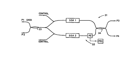
Figure 3 shows a first example of an optical
demultiplexer embodying the present invention. The
demultiplexer is configured as a Mach-Zehnder
interferometer having first and second arms 31, 32.
Respective semiconductor optical amplifiers SOA1, SOA2 are
connected in each arm. Inputs are provided in each arm for
a control signal going to each SOA. In use, the data pulse
stream at ~3 is input at one port Pl of an input coupler
CA 022l0~36 lss7-07-l~
W096/22562 ~CT/GB96/00072
33. This is a 50:50 directional coupler which splits the
input signal equally between the two arms of the
interferometer. After passing through the SOAs the optical
signals are recombined at the output coupler 34 and output
from one or other of its two ports P3, P4 depending upon
the differential phase shift produced by the SOAs.
Whereas in the prior art the differential phase shift
was produced by the use of data pulses arriving at
different times at the SOA, using the configuration of the
present invention this is not necessary. The data pulses
can arrive simultaneously at the SOAs and so the bit rate
of the data pulses is not limited by the transit time of
the SOAs. The differential phase shift is achieved by the
use of a time off-set between sequences of control pulses
applied to the different SOAs. A planar optical delay line
may be used to split a control signal from an appropriate
source to provide two control pulse streams with a
predetermined delay between them. Referring to Figure 4,
where curve A is the phase of SOA1 and curve B is the phase
of SOA2, then a control pulse arrives at SOAl at instant
Tl. The corresponding control pulse for SOA2 is delayed so
that it arrives at a later instant T3. The timing of these
control pulses and their relative delay are chosen so that
they bracket the arrival of a data pulse at the SOAs at
time T2. At that time SOAl has just been depleted by the
control pulse, while SOA2 has not yet received the control
pulse. The different portions of the pulse in SOAl and
SOA2 therefore experience different phase shifts, producing
a phase differential of ~. As a result of this phase shift
when the portions are recombined in the output coupler 34
this selected pulse is output from port P3. By contrast,
a later arriving data pulse at time T5 experiences only a
small differential phase shift ~ and so is output almost
entirely from port P4.
The residual differential ~ is eliminated entirely so
that for data pulses other than the selected pulse the
phase differential is zero. This is achieved by adding in
CA 02210~36 1997-07-1~
W096/22562 PCT/GB96/00072
one of the arms of the interferometer a phase shifting
element PE which adds a permanent phase differential equal
to ~. Then, the demultiplexer produces an optimum total
differential phase shift of ~ for the selected pulses and
0 for the other pulses. The addition of the phase shifting
element PE is equivalent in effect to shifting curve B
upwards by ~, thereby eliminating the difference in the
phase shift experienced by the pulse portions in the
different SOAs at, e.g., time T5.
The phase shifting element PE may be formed, for
example, from a length of germanium-doped silica waveguide
having a length and doping level chosen to provide the
desired phase shift. Alternatively the element PE may be
formed from a photosensitive glass. Then in the
fabrication of the circuit, after the completion of the
other elements, the switch may be operated and the output
levels from one or other of the output ports P3, P4
monitored. The photosensitive glass is then illuminated at
an appropriate ultra-violet wavelength and the intensity of
the illumination increased until the monitored circuit
output from P3 and/or P4 is optimised. An appropriate
photosensitive glass for these purposes is described in
reference (3) cited on page 10 below.
In some fields of use it may be desirable for the
phase element PE to be adjustable after fabrication. In
this case it may take the form of an electro-optic element
such as a lithium niobate cell. Alternatively the element
may be provided by a further semiconductor optical
amplifier whose phase delay is adjustable by adjusting its
electrical drive current. Where such an adjustable phase
element PE is used, then a control circuit (PEL) using a
feedback loop from the output of the switch may be used to
provide the control signal to the phase element to ensure
that the phase differential is always optimally cancelled.
The control circuit may include a photodetector which
detects the output of the switch.
CA 02210~36 1997-07-1~
W096/22562 PCT/~9G/00072
Typically the pulses to be selected by the
demultiplexer will be one or more time slots corresponding
to specific OTDM channels at a bit-rate of, e.g., 100
Gbit/s. In the example shown in Figure 5, channel 1 of
four channels is to be selected. The control pulses
therefore comprise a sequence with a period equal to the
OTDM frame period. The time off-set between the pulses
applied to SOAl and SOA2 is chosen to be greater than the
data pulse width but less than the data bit period. It can
be seen that any other arbitrary channel may be selected by
advancing the timing of the control pulses appropriately
with respect to the data pulses.
Figure 6 shows a circuit implementing the multiplexer
shown schematically in Figure 3. This is a hybrid circuit
combining planar silica technology with discrete
semiconductor components for the SOAs. Each SOA is an InP-
based semiconductor laser amplifier with the gain medium
angled at 10~ with respect to the faces of the silica
substrate and tapered at its ends. Where the SOA is, for
example, 2mm long, then the gain medium has a taper of
500~m length at each end. In this example, the width of
the gain medium reduces from 1.3~m to 0.2~m along the
length of the taper. These SOAs are sandwiched between a
pair of planar silica circuits which provide the input and
output ports of the demultiplexer as well as the couplers
and splitters illustrated in Figure 3. The tapering of the
SOA gain medium at its ends improves the efficiency of the
mode coupling between the SOA and the silica circuit. The
angle of the SOA gain medium with respect to the normal to
the end faces of the SOA, and of the waveguides, serves to
reduce internal reflections, which otherwise might cause
feedback in the devices
The couplers in this example, are all directional
couplers arranged to provide a 50:50 coupling ratio. On
the input side of the planar silica there are provided
input ports for a holding beam H and control signal C
respectively for the first SOA and a corresponding pair of
CA 022l0~36 l997-07-l~
W096/22562 PCT/GB96100072
inputs for the second SOA together with an input for the
data pulse stream D. On the output side there are
corresponding output ports for control and holding beams
together with the straight-through and cross-over output
ports for the data.
In an alternative configurati~n shown in Figure 6b, a
looped path may be provided in the silica for the holding
and control beams using a reflection grating etched in the
waveguide core between pairs of directional couplers.
Alternatively, a photo-refractive grating might be used.
The two directional couplers CO1, C02 and the arms of the
waveguides between the couplers are in the form of a Mach-
Zehnder interferometer and the reflection gratings control
the phase bias of the different arms of the interferometer.
The bias is set so that both of the input signals C and D
are output from a single arm of the interferometer system
and fed to the SOA. This system allows coupling of C and
D with close to 100~ efficiency. Where a holding beam H is
- used, then this in general will be at a different
wavelength for which the grating functions as a reflective
grating. The holding beam may be longer or shorter in
wavelength but within the gain bandwidth of the SOA, which
is typically around 50nm. The data pulses may be within
the gain bandwidth or at longer wavelengths. As shown, H
is introduced into the coupler/interferometer system in the
opposite direction to the data and control signals.
Circuits of this type are described in further detail in:
(1) "Integrated four channel Mach-Zehnder
multiplexer/demultiplexer fabricated with phosphorous
doped sioz waveguides on Si" by Verbeck et al, Journal
of Lightwave Electronics pplO11-1015, 6(6), '88.
(2) "Silica-based integrated optic Mach-Zehnder
multiplexer/demultiplexer family with channel spacing
of .01-250nm" by Takato et al, IEEE Journal on
selected areas in communications, ppll20-1127, 8(6),
'90 .
CA 022l0~36 Iss7-07-l~
W096/22562 PCTIGB96/00072
(3) "Laser-trimmed four-port bandpass filter fabricated in
single-mode photosensitive Ge-doped planar waveguide~
by Kashyap et al, IEEE Photonics Technology Letters,
pp 191-194, 5(2), Feb '93.
It should be noted in relation to this and to the
other embodiments described that the use of a holding beam
H is not essential, but may be omitted. In many
circumstances, sufficient switching speed can be obtained
simply by appropriate electrical bias of the SOAs without
use of an optical holding beam.
In this example, the waveguide channels in the planar
waveguide have a width and depth of 5 microns and a
refractive index gradient ~n=0.01. As shown in Figure 7,
at the interface with the SOAs the facet of the silica
waveguide is angled at 22~~. This geometry combined with
the tapering of the core of the SLA at its ends to provide
mode matching between the SOA active channel and the
waveguides ensures maximum coupling efficiency between the
planar circuits and the SOA devices.
The switch of the present invention is by no means
limited in use to optical demultiplexing. Another
important field of application is in optical clock
recovery. Our above-cited earlier International
application describes and claims a number of circuits for
recovering a timing waveform for use in subsequent
processing of an optical signal. The circuits are based
upon the use of a non-linear optical modulator (NOM)
connected in the optical cavity of a mode-locked laser.
The optically encoded signal is applied to the optical
modulator and modulates the phase and/or amplitude of light
in the optical path of the laser cavity thereby locking the
phase and frequency of the output pulse stream to the
timing wave of the optically encoded signal. Figure 8
shows a clock recovery circuit using the optical switch of
the present invention as the non-linear optical modulator.
The switch of Figure 3 in this case is connected into the
optical cavity of a fibre-ring laser via ports P2 and P4.
CA 022l0536 Iss7-07-ls
W096/22562 PCT/~b'jG~'C0072
The control signal for the SOAs is derived by splitting the
input datastream (that is the stream from which the clock
is to be recovered) and applying it to the two SOAs via an
optical delay line to give the required delay. The output
coupler 834 is chosen to provide, e.g., a 60:40 splitting
ratio between ports P3 and P4. Accordingly the switch in
effects modulates the amplitude of the output signal
depending on which port it is switched to.
The other components for the clock recovery circuit
are conventional and are described in further detail in our
above-cited International application. In the example
shown in the Figure, they include an isolator and an Er-
doped fibre amplifier. Alternatively, the mode-locked
laser may use a Semiconductor Laser Amplifier to provide
the active medium, and in this case advantageously the SLA
and the switch may be formed as an integrated semiconductor
device.
A further use for the switch is in an "all-optical"
oscilloscope or other test instrument. In this case the
switch acts as a correlator. A circuit in the form shown
in Figure 3 is used, with an optical signal to be sampled
input at port Pl. The control signal is then a repetitive
optical signal with a frequency different from but close to
the repeat period of the data to be sampled. There is then
a "walk-through" effect as the switch samples and outputs
from port P4 successive portions of the signal input at P1.
The switch of Figure 3 may be used with a continuous
wave input at Pl rather than a pulsed datastream. The
switch then functions as a pulse width modulator with the
width of an output pulse from P4 determined by the relative
delay between the two input control signals.