Note: Descriptions are shown in the official language in which they were submitted.
CA 02210922 1997-07-21
-1-
Method And Apparatus For Tracking Alignment
In Wireless Optical Communications
Background of the Invention
This invention relates to optical communications, and more particularly
to a method and apparatus for tracking alignment in optical communications
systems.
Optically-based wireless transceiver systems have provided
revolutionary advancements in the field of communications. Such systems have
become increasingly prevalent and have been implemented for many practical
applications. For example, optical communications are used for data gathering
functions such as video-conferencing, E-mail, fax, television, digital radio
communications, and a variety of networking applications. The popularity of
optical
systems can be attributed to their numerous beneficial characteristics.
Optical
systems are wireless; thus, physical installation is relatively simple. Noise
and
interference problems associated with other types of wireless communications
have
largely been eliminated with the advent of optical systems. The total power
consumption for most optical systems is comparably low. These and other
benefits
have made wireless optics an increasingly popular communication technique.
One shortcoming of existing wireless optical systems is the requirement
that the transmitting source be properly aligned with the receiving source.
Without
proper alignment, the optical receiver cannot effectively evaluate the optical
beam to
perform data recovery. The problem is exacerbated where substantial electrical
noise in the environment interferes with the optical receiver. Such
interference may
falsely trigger the system to recognize an optical beam when none was in fact
transmitted. In contrast, systems using hardware connections, such as fiber
optics
systems, do not require transmitter-receiver alignment. The transmitted wave
simply
follows the contour of the wire or other transmission media until it reaches
the
receiver.
Nevertheless, a wireless optical receiving system having a very efficient
correction mechanism would minimize alignment problems while preserving the
remaining substantial benefits associated with wireless optical
communications.
Also, for maximum efficiency, it ~is desirable to implement an optical
system which can effectively process a low-energy optical beam. Having such a
system, low power optical signals can be transmitted and decoded at the
receiving
end such that a minimum amount of energy is expended in the process.
CA 02210922 1997-07-21
-2-
To perform these tasks, an optical communication system must be
capable of automatically realigning the transmitter and receiver which, for
whatever
reason, have become misaligned. Unfortunately, current technology requires
that
multiple receiving elements be used for receiver realignment and data
gathering.
The use of multiple elements, among other things, increases cost and power
consumption while decreasing overall system efficiency.
As an illustration, one prior art optical receiving communication system
uses a separate quadrant sensor, positioned in the line-of-sight of the
optical
transmitter, to detect and correct alignment errors. The system also uses a
collecting
lens to project the received beam onto a photodiode for data recovery.
Disadvantageously, this approach requires at least three distinct elements (a
quadrant
sensor, a collecting lens, and a photodiode) to implement the system's optical
receiver. Thus, multiple optical receiving elements are required to implement
data
recovery and directional accuracy tracking, which complicates and increases
the cost
of the receiving system. Another disadvantage of this system is its
inefficient use of
transmitted optical power. In particular, after evaluating the alignment
accuracy of
the transmitted beam, the quad sensor must then permit photons of the beam to
pass
through the sensor to a second apparatus (collecting lens and photodiode) for
data
recovery. The transmitted beam must contain sufficient signal power to enable
the
beam to pass enough photons to the photodiode through a small aperture in the
quad
sensor. This prior art configuration places practical limits on the minimum
achievable transmitted signal power. While further drawbacks to this prior art
approach are omitted from discussion, they will be apparent to practitioners
in the
art.
It is therefore an object of the invention to provide a more simplified,
compact and robust method and apparatus for processing received optical
signals.
It is still another object of the invention to provide a method and
apparatus for using a single optical receiving element to perform both data
recovery
functions and tracking accuracy evaluations.
It is further an object of the invention to provide a more efficient optical
communication system which requires less power consumption than existing
systems.
CA 02210922 2000-OS-25
-3-
. ummar~r of the Invention
These and other objects of the invention are accomplished in accordance
with the principles of the invention by providing a method and apparatus which
uses
a single array sensor to receive transmitted data and to determine tracking
accuracy.
The array sensor, which is the principle data recovery mechanism, receives an
optical beam from a transmitting source such that a projected image of the
received
beam is captured on the array. The projected image is compared with a
predetermined image to determine tracking accuracy of the received beam.
Deviations between the projected image and the predetermined image alert the
system that a tracking error has occurred, and corrective action to realign
the
receiver with the transmitter may be initiated based on the error.
In accordance with one aspect of the present invention there is provided
an optical communications system comprising: a transmitting element; and a
receiving element, said receiving element comprising a CMOS image sensor array
for determining tracking accuracy of an optical beam transmitted from said
transmitting element and for detecting data, said data comprising bits per
time slot,
each bit being detected as a number of photons per pixel, the number of
photons per
pixel being recorded as a digital bit when the number of photons exceeds a
predetermined threshold.
In accordance with another aspect of the present invention there is
provided an optical communication receiving system for tracking beam
alignment,
comprising: an array sensor for receiving an optical beam from a transmitting
source, wherein the system compares a planar shape of an illuminated image on
said
array sensor created by the impact of said optical beam, with a planar shape
of a
predetermined image, and wherein the system initiates corrective alignment
between
the transmitting source and said array sensor upon detecting a deviation in
only one
of two dimensions between the shape of said image and the shape of said
predetermined image.
In accordance with yet another aspect of the present invention there is
provided an optical communications system for evaluating alignment accuracy,
comprising: a transmitter comprising a laser source for transmitting an
optical
beam; and a receiver comprising an array sensor which receives the optical
beam,
the optical beam impacting said array sensor, an image having a two
dimensional
CA 02210922 2000-OS-25
- 3a -
shape being formed on said array sensor by the impact of the optical beam, the
elongated shape of the formed image in comparison with a predetermined two
dimensional shape being used to determine whether said array sensor is aligned
with
said transmitter.
In accordance with still yet another aspect of the present invention there is
provided an optical receiving element comprising an array sensor comprising an
array of light gathering devices, said receiving element used to recover data
based
on the presence or absence of an optical beam impacting said array sensor, and
said
receiving element used to concurrently measure alignment errors based on the
elongated nature of the two dimensional shape of an impacting optical beam in
comparison with a predetermined two dimensional shape.
In accordance with still yet another aspect of the present invention there
is provided a method for tracking alignment using an optical communication
system,
comprising the steps of receiving an optical beam from a transmitting source
by
impacting the optical beam onto an array; comparing a two dimensional shape of
the
impacted image with a two dimensional shape of the predetermined image;
determining whether a deviation in one of said two dimensions of said two
dimensional shape exists between the shapes of the respective images; and
initiating corrective alignment based on a direction and extent of a deviation
between the shapes of the respective images.
In accordance with still yet another aspect of the present invention there
is provided an optical communication receiving system for tracking beam
alignment,
comprising: an array sensor for receiving an optical beam from a transmitting
source comprising an array of photodiodes for sensing the presence or absence
of
pulses, wherein the system compares a shape of an illuminated image on said
array
sensor created by the impact of said optical beam with a shape of a
predetermined
image, and wherein the system initiates corrective alignment between the
transmitting source and said array sensor upon detecting a deviation between
the
shape of said image and the shape of said predetermined image, wherein data is
communicated over a plurality of time slots by the impact or lack of impact of
the
optical beam onto said array sensor, and wherein the system sums for each time
slot
the number of pixels on said array sensor impacted by the beam, the impact of
the
beam onto a pixel being represented by a first data value and the absence of
impact
being represented by a second data value.
CA 02210922 2000-OS-25
-3b-
In accordance with still yet another aspect of the present invention there
is provided a method for tracking alignment using an optical communication
system,
comprising the steps of receiving an optical beam from a transmitting source
by
impacting the optical beam onto an array; comparing a shape of the impacted
image
with a shape of the predetermined image by summing the pixels on said array
which
have been impacted by the beam, comparing the sum with a predetermined
threshold
number and recording the distribution of impacted pixels into a memory where
the
sum meets or exceeds the threshold number; determining whether a deviation
exists
between the shapes of the respective images; and initiating corrective
alignment
based on a deviation between the shapes of the respective images.
Further features of the invention, its nature and various advantages, will
be more apparent from the accompanying drawings and the following detailed
description of the preferred embodiments.
Brief Description of the Drawing
FIG. la is a simplified representation of an illustrative prior art optical
communication system.
FIG. lb is a front view of a prior art quad sensor used in the optical
communication system of FIG. 1 a.
FIG. 2a is a simplified representation of an illustrative embodiment of
an optical communication system using a single array sensor, in accordance
with the
present invention.
FIG. 2b is a view of an array of light gathering devices comprising the
array sensor of FIG. 2a.
FIG. 2c is an orthogonal view of the array sensor of FIG. 2a.
FIG. 3 is a simplified representation of an illustrative alignment tracking
technique in accordance with a preferred embodiment of the present invention.
FIG. 4 is a conceptual diagram which illustrates geometric invariance
with respect to several projected images of varying magnitude and direction.
FIG. 1 a depicts a prior art system for receiving optical communications.
The system is generally characterized by two transceiver stations positioned
at some
spatial distance from each other. One transceiver station comprises a
transmitting
CA 02210922 1997-07-21
-4-
element 150, which includes laser source 100 and collimating lens 110. The
collimating lens 110 produces a circular projection of the transmitted beam.
The
other transceiver station comprises a receiving element 160, which includes
photodiode 140 and collecting lens 120. An optical beam is transmitted from
laser
source 100 in the line of sight of receiving element 160. Collecting lens 120
deflects
the impacting beam into photodiode 140 for further processing. Photons
residing in
the optical beam are used to transmit digital information to receiving element
160.
Photodiode 140 measures characteristics of photons from the beam. Such
measurements are used to recover information conveyed from transmitting
element
150 to receiving element 160. Typically, the presence or absence of a beam in
a
given time slot signifies either a logic zero or a logic one.
To effectuate reliable data recovery, proper alignment is required
between transmitting element 150 and receiving element 160. Practitioners have
conventionally deployed a quadrant sensor ("quad" sensor) 130 for this
purpose.
FIG. lb is an orthogonal view of the quad sensor 130 of FIG. la, which shows
the
circular aperture 146 into which the optical beam passes through sensor 130 to
contact photodiode 140. Quad sensor 130 relies on four spatial quadrants, 15,
16, 17
and 18, to determine whether receiving element 160 (i.e., the collecting lens
120 and
photodiode 140 of FIG. 1 a) is properly aligned with laser source 100 such
that a
precise transmission of the optical beam is effected.
The impacting photons created by the optical beam cause charge to
accumulate on the four spatial quadrants 15, 16, 17, and 18 of quad sensor 130
(FIG.
lb). The optical system periodically measures the relative difference in
charge
concentration between diametrically opposed quadrants. For vertical alignment
adjustments, the difference between the respective charge concentrations in
quadrants 17 and 18 is measured. Similarly, for horizontal alignment
adjustments,
the difference between the respective charge concentrations in quadrants 15
and 16 is
measured. These differences in accumulated charge between two quadrants are
called the differential outputs. Where the differential outputs are zero, the
charge
concentration is uniform throughout the four quadrants, which indicates that
receiving element 160 is properly aligned with laser source 100.
In the normal course of operation, the optical system periodically
measures the two differential outputs. Based ~on these periodic measurements,
the
system intermittently realigns the receiving element 160 so as to maintain the
value
of the differential outputs near zero. For quadrants 17 and 18, the magnitude
of the
differential output governs the magnitude of vertical adjustment of receiving
element
CA 02210922 1997-07-21
-5-
160 required to restore proper alignment with the transmitted beam. Similarly,
the
differential output measured from quadrants 15 and 16 controls the required
magnitude of horizontal adjustment. The differential output may be positive or
negative depending on the frame of reference chosen for the measurements.
Whether the differential output is positive or negative determines the
direction of the
required adjustment,(i.e., left or right for horizontal measurements; up or
down for
vertical measurements).
In the exemplary quad sensor of FIG. lb, quadrant 17 is given a positive
frame of reference relative to quadrant 18, and quadrant 15 is given a
positive frame
of reference relative to quadrant 16. If the concentration of charge in
quadrant 17 is
greater than in quadrant 18, the system will measure a positive differential
output.
This signifies that an upward vertical adjustment to the receiving element 160
is
necessary. The amount of realignment needed is proportional to the magnitude
of
the differential output obtained from quadrants 17 and 18.
Horizontal alignment is accomplished in a similar manner. The system
measures the difference between the concentration of charge in respective
quadrants
15 and 16. If, for instance, the measured concentration of photons in quadrant
16 is
greater than that of quadrant 15, a negative differential output is obtained,
which
means that a receiver adjustment to the left is necessary. The amount of
horizontal
receiver adjustment is directly proportional to the differential output
obtained from
quadrants 15 and 16.
Based on the respective differential outputs obtained from the two pairs
of quadrants, the optical communication system will actuate realignment using
some
known method such as with physical actuators. While the system realigns the
receiving element 160 with the transmitting element 150, photodiode 140
continues
data recovery by sensing either the existence or absence of photons from the
transmitted optical beam. The data recovery method relies on photons which are
passed through quad sensor 130 via aperture 146 onto photodiode 140.
As previously explained, the communication technique of Figs. 1 a and
lb requires the use of multiple optical receiving elements to perform the dual
tasks
of alignment tracking and data recovery. Because the beam must be processed by
a
quad sensor, and then passed through to the collecting lens for further
processing, the
use of multiple elements results in a less efficient use of the transmitted
power.
Using multiple elements also results in an optical communication system which
is
bulkier, more difficult to deploy in environments having limited space, more
costly
due to additional power consumption and the added expense of the individual
CA 02210922 1997-07-21
-6-
elements, and less immune to spurious electrical interference. Additionally,
where
multiple elements work concurrently to provide both the necessary tracking
alignment and data recovery functions, tracking alignment can be a
particularly slow
process. The quad sensor can also produce alignment errors where identical
misalignments occur in the right and left quadrants and the up and down
quadrants,
respectively.
The present invention, described below in the context of the inventor's
presently preferred embodiments, provides both a more compact approach to
optical
communications and a more efficient, unitary use of transmitted power.
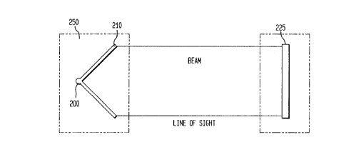
Referring to
FIG. 2a, a preferred transceiver arrangement is shown in accordance with the
present
invention. A laser source 200 and a collimating lens 210 comprises the
transmitting
element 250. Source 200 sends an optical beam using collimating lens 210 to
circularize the image. A single array sensor 225 comprises the receiving
element.
Array sensor 225 generally comprises an array of light gathering rlevices.
Although
it may comprise any suitable light-gathering device, array sensor 225
preferably
comprises an array of photodiodes arranged in rows and columns. Where
photodiodes are used as the light-gathering mechanism, each photodiode is
considered to comprise an individual pixel on array sensor 225. The output of
each
photo diode is typically coupled to an electronic control mechanism, the
details of
which are not critical to an understanding of the invention. The photodiodes
comprising each pixel are used to detect the presence or absence of photons
residing
in an impacting beam. This information, in turn, is used to establish the
existence
and shape of a transmitted optical beam in a manner to be described below.
Unlike prior art systems wherein a collecting lens 120 is required (see
FIG. 1 a), a collecting lens need not be used in the present invention. The
optical
beam instead strikes array sensor 225 directly, causing the image created from
the
laser source 200 to be collimated directly on sensor 225. The system may then
make
alignment measurements and extract data by evaluating the image illuminated on
the
array sensor 225.
FIG. 2b is an illustrative view of the surface of array sensor 225, having
a plurality of photodiodes 400 arranged in rows and columns as in some
embodiments of the invention. In these embodiments, control system 475 has a
row
address and a column address dedicated for each respective row and column of
the
array. By referencing a particular row address and column address, control
system
475 can read the output of photodiode on the array. The row and column
addresses
can be stored in a memory 450 in control system 475. In the illustration of
FIG. 2b,
CA 02210922 1997-07-21
_7_
control system 475 is referencing a particular row address and column address
to
read the output at photodiode 500 on the array.
FIG. 2c shows an orthogonal view of array sensor 225 in a flat
rectangular form. However, alternative shapes of array sensor 225 may be
contemplated.
Data recovery may beneficially be performed concurrently with the
alignment analysis using the same array sensor 225. In a preferred embodiment,
discrete time slots exist wherein each time slot corresponds to a specific
digital
value, i.e., a logic one or a logic zero. In this embodiment, the transmission
of a
beam in a time slot indicates the existence of a logic one. Conversely, the
absence of
transmission in a time slot indicates the existence of a logic zero. Data is
accordingly recovered as one digital bit per time slot. When a beam is
transmitted
from laser source 200 (FIG. 2a), the existence of photons striking sensor 225
delineates the areas of impact which, in turn, establishes the shape of the
beam. The
beam may be used for alignment evaluations (see below). The impact of the
photons
on sensor 225 also enables the system to extract data sent by the beam. Data
may be
recovered by adding, for each time slot, the net number of pixels on sensor
225
which have been impacted by photons from the optical beam. Using this summing
procedure, the transmitted information is collected for communication to a
central
controller or other designated location. The system controller then processes
this
information offline to perform data recovery and tracking alignment functions.
As
such, the single array sensor 225 advantageously performs the dual functions
of data
recovery and tracking alignment.
A preferred embodiment of the data recovery technique of the present
invention uses a CMOS image sensor as the array sensor 225. A CMOS image
sensor comprises a plurality of photodiodes arranged in row and column format,
like
the array depicted in FIG. 2b. Each photodiode comprises an individual pixel
of
array sensor 225. One advantage of using a CMOS image sensor 225 over other
devices, such as a charge-coupled device (CCD), is that it may read the output
at
individual pixels, thereby significantly increasing data recovery times.
Specifically,
for each time slot, the image sensor 225 measures the number of photons
impacting
each pixel located on array sensor 225 as follows. The system control
mechanism
preferably comprises a memory which stores row and column addresses as
described
above. The system controller addresses each pixel by selecting a particular
row
address and column address. Using these row and column addresses, the system
controller reads the contents at each pixel output. The digital value of the
pixel
CA 02210922 1997-07-21
_$_
output will depend on the amount of photons which have impacted that pixel
during
a particular time slot. In the case where a beam has been transmitted in that
time
slot, the photon concentration at each photodiode will be high. Conversely,
where
no beam has been sent, the photon concentration at each photodiode will be
markedly lower. Thus some threshold quantity of photon concentration exists
below
which the output of tile photodiode will have a first digital value, and above
which it
will have a second digital value. Where a high concentration of photons on a
photodiode (indicating the presence of a beam) yields a second digital value
at that
pixel's output, the system controller will flag that pixel. Alternatively,
where a
lower concentration of photons on a photodiode yields a first digital value,
the pixel
is not flagged. The use of a CMOS image sensor in this context has at least
two
advantages: (1) pixels not impacted by the optical beam are eliminated from
the
subsequent summing step (see below); and (2) pixels which have been impacted
by
spurious electrical noise, but which have not been impacted by the optical
beam will
not meet the photodiode threshold (if the threshold is chosen properly), and
likewise
are not considered for summation.
Next, the summing procedure described above is employed wherein the
number of flagged pixels are summed by a system controller. If the sum total
of
flagged pixels surpasses a second predetermined threshold number, the system
concludes that an optical beam has been transmitted (as opposed to either no
transmission or mere electrical interference without a transmission), and
accordingly
assigns a digital one for that time slot. Conversely, if the sum total of
flagged pixels
does not exceed the predetermined threshold number, the system determines that
no
optical transmission has occurred and assigns a digital zero for that time
slot. This
summing procedure may occur for any number of time slots, and a string of
digital
information is obtained from the transmitting element 210. Of course, the
digital
values may be reversed, where the presence of a beam instead yields a digital
zero,
etc.
The system controller may also record in memory the distribution of
impacted pixels for alignment measurements (see below). In some embodiments,
such information is stored only where the sum total of impacted pixels meets
or
exceeds the predetermined threshold number.
This preferred data recovery metl~nd using a CMOS image sensor has
distinct advantages. First, image sensor 260 significantly increases the rate
of data
recovery as compared with previous methods. For example, conventional data
recovery devices, such as Charge Coupled Devices (CCD) used in instruments
like
CA 02210922 1997-07-21
-9-
camcorders, necessitates reading the entire pixel array before evaluating
individual
pixels. This procedure results in comparably long data recovery times. In
contrast,
CMOS image sensor 160 provides for the reading of individual pixels without
requiring an assessment of the entire array. Moreover, unlike a system using a
CCD,
only those pixels selected by image sensor 160 need be considered by the
system
controller. The remaining pixels are simply discounted from the summing step.
Hence, the computation time relating to the summing procedure is considerably
faster than if all pixels were summed. Using such a device, data recovery
rates of 1
Gbps or greater can be achieved. This data recovery time is comparable to, or
better
than, optical communication techniques which employ a quad sensor.
The use of a CMOS image sensor provides further benefits in terms of
resistance to noise. Spurious electrical transmissions which trigger minimal
photon
activity on a given pixel are readily discounted by the image sensor. Thus the
effect
of noise is minimized, and more accurate data measurements are obtained.
The above illustrations, and each of the above techniques, represents the
preferred method of implementing data recovery using array sensor 225. Other
equally suitable techniques and variations may be contemplated by those
skilled in
the art after perusal of this disclosure.
For alignment measurements, the transmitted optical beam impacts the
array sensor 225, and thereby illuminates an image on sensor 225. The
preferred
method of reading the individual pixel outputs, described above, is likewise
used by
the system in determining the shape of a transmitted beam for performing
tracking
alignment. In particular, the system determines the shape of an impacting beam
by
evaluating the number and position of pixels which have been impacted by
photons.
Preferably, information relating to the distribution of impacted pixels (which
establishes the shape of the impacted image) is placed in a memory to await
further
processing. The system compares this illuminated image with a predetermined
image to determine whether deviations exist between the two. The presence of
deviations indicates that corrective measures need be taken to align the
transmitter
and receiver. The magnitude and direction of the corrective measures are
proportional to the magnitude of deviation of the illuminated image from the
predetermined image.
Advantageously, the information obtained during the data recovery
process, and specifically the information obtained from image sensor 260 about
each
pixel, may also be used to measure alignment accuracy. For instance, the shape
of
the projected image onto sensor 225 is determined based on the distribution of
CA 02210922 1997-07-21
- 10-
impacting photons on array sensor 225 as described above. The shape of this
image
yields important information about alignment accuracy (see below).
Array sensor 225 determines whether a misalignment exists between
itself and transmitting element 250. This determination is made without the
need for
additional alignment detection structures. Upon determining alignment errors,
sensor 225 provides necessary information to a system controller or other
source.
Using this information, the system may make corrective measures to promptly
restore proper alignment for the continued and accurate reception of
transmitted
data.
The realignment mechanism of the present invention relies in part on the
known principle of geometric invariance under perspective transformation. This
principle decrees that a projected circle will image as a circle, but only if
the image
is projected orthogonally (that is, perpendicularly) relative to the screen.
In all other
cases, the projected circle will image as an ellipse. Thus, where a circular
beam
from a transmitting source is projected under circumstances where the
transmitter is
not perfectly aligned with the receiver, the image will consequently appear as
an
ellipse to the transmitting source. Further, the specific contour of the
ellipse
beneficially conveys information relating to the nature and extent of the
misalignment.
Applying this principle to the present invention, orthogonal alignment
between transmitting element 250 and array sensor 225 results in the
collimated
beam imaging as a circle onto sensor 225. Thus, where sensor 225 perceives a
circle
being imaged onto it (e.g., using the CMOS image sensor technique), alignment
is
deemed correct, no corrective action is taken, and data recovery commences as
usual.
Where the projected image instead appears as an ellipse, the system
concludes that a misalignment exists between transmitter and receiver. The
degree
of divergence from a circular shape and the shape of the projected image
provides
the system with information relating to the direction and extent of
misalignment.
Using this information, the system may adjust the alignment of the sensor 225
in a
manner proportional to the magnitude and direction of the misalignment of the
optical beam. Thus, the simple projection of the imaged beam onto receiving
sensor
225 enables the system to take corrective measures in response to deviations
in
alignment.
Associated with the array sensor, and contained within the system, is a
predetermined image for comparison with the image impacting array sensor.
Where
a circular beam is projected, for example, the predetermined image will be a
circle.
CA 02210922 1997-07-21
-11-
Other geometries are intended to be within the scope of the invention.
FIG. 3 is a conceptual diagram which illustrates the use of geometric
invariance on projected images. The image projected onto array sensor 325 is
examined, and the extent to which the image deviates from a circle is
determined in
both horizontal and vertical directions. Boxes 345 represent orthogonal views
of
array sensor 325. Ensuing alignment corrections by the system are proportional
to
the magnitudes of horizontal and vertical deviations from the circular shape.
In
some embodiments, physical actuators are used to realign the receiver with the
transmitter.
FIG. 4 is a conceptual diagram which illustrates geometric invariance
with respect to several projected images of varying magnitude and direction.
The
circles labeled 501 represent an instance in time where the transmitting and
receiving
elements are perfectly aligned. In this case, the composite image will result
in circle
502, in which event no realignment need be effectuated by the system. The
other
circles 600 comprising the vertical and horizontal projected image are
displaced
from the center of the array sensor. As such, each pair of those images (one
vertical
and one horizontal) represent individual instances in time where alignment is
imperfect. Depending on the magnitude and direction of the misalignment, the
composite image will appear as an ellipse rotated on a diagonal. The extent
and
direction of misalignment are proportional to the degree of rotation of the
composite
image. In response to the shape and degree of rotation of the composite image,
the
system can then take corrective action to realign the receiving element with
the
transmitting element.
Ambiguities of sensor 225 in interpreting alignment are resolved at the
outset by properly calibrating the system upon installation. Initial
calibration is
necessary to avoid misalignment of the image by an identical amount to the
left and
right of the projected image, which would otherwise produce alignment errors
due to
the similarity of produced right and left images. Likewise, initial
calibration solves
the problem which occurs when misalignment by an equal amount up and down
results in similar ellipses causing similar images which would otherwise
produces
ambiguities in alignment. Initial system calibration enables the misaligned
image to
be projected onto a different quadrant of the array sensor such that left-
versus-right
or up-versus-down misplacements are vividly'distinguishable. Thus, in the
initial
installation, the rough location of the source is preferably ascertained, and
a center is
established relative to the communication system. Based on this initial
centering,
the system can evaluate the resulting ellipse to determine the true amount of
CA 02210922 1997-07-21
- 12-
displacement, and accordingly make alignment corrections.
In addition to projecting the beam as a circle, other shapes may be
contemplated. The principle of geometric invariance dictates that a non-
orthogonal
projection of a beam having a predetermined shape will result in the beam
impacting
a source with a different shape. Thus, for example, the practitioner may
choose to
shape the beam as a rectangle, and then use the principles of geometric
invariance
and the present invention to ascertain the extent of misalignment at the
receiving
end, making appropriate corrections.
It will be understood that the foregoing is merely illustrative of the
principles of the invention, and that various modifications can be made by
those
skilled in the art without departing from the scope and spirit of the
invention. All
such variations and modifications are intended to fall within the scope of the
claims
appended below.