Note: Descriptions are shown in the official language in which they were submitted.
CA 02211071 1997-07-21
-1-
MiTLTILAYER li'IJS>JY} MiCROWAVE C4tVi}ICTI'VF STRUC'TU1ZF
F'eIi d ofThe Invention
The present invention relates generally to the field of microwave conductive
strucuzres for
improving the cooking, heating or browning of food in microwave ovens. More
particularly, the
invention relates to articles usable in conventional food packaging which
interact with
electromagnetic energy generated by the microwave oven and adapt to different
microwave oven
types, food compositions and food geometries.
BaCk.groUnd
An example of a microwave conductive structure is a microwave susc:,ptor which
is an
article which absorbs microwave energy, eanverts it into heat and conducts the
heat generated
into food articles placed in close proximity thereto. Microwave susceptors are
particularly useful
in microwave food packaging to aid in browning or crisping those foods which
are preferably
prepared by a method which browns or crisps the food.
The field of microwave conductive packaging technology inciudes numerous
attempts to
optimize heating, browning and crisping of food cooked in microwave ovens.
Such attempts
include the selectively miczowave-permeable membrane susceptor shown in prior
U.S. patent
number 5,185,506, issued February 9, 1993 and U.S. patent number 5,245,821
issued October
19, 1993. Other attempts include a microwaveable barrier film described in
L'.S.-patent number
5,256,846 issued October 26, 1993 and a microwave diffu.ser film described in
U.S. patent
number 5,300,746 issued Apri15, 1994. U.S. patents 5,185,506 and 5,245,821
disclose examples
of constructions whicli modify the overall heating pattern in a;nicrowave oven
in an attempt to
optimize the heating for a specific food product and geometry. However, these
and conventional :
microwa.ve susceptor structures do not adequately address the heating problems
associated with
non-unii'orm electromagnetic fields found in all microwave ovens.
The unpredictability of the microwave field within a mierowave oven is a
significant
problem foz articles and methods which attempt to make heating, browning or
crisping of food
uniform. There are morc than 500 models of microwave ovens on the market
today, all of which
AMENDED SHEET
CA 02211071 1997-07-21
-2-
have different heating patterns and r,on-unifbrm energy fields. Since most
food products
themselves are non-uniform in size and shape, there is an increased natural
tendency of food to
heat unevenly. The inability to adequately predict locations of hot spots and
cold spots within a
microwaved, packaged food item including a susceptpr has made this area the
subject of much
research. For example, fishsticks or french fries loosely packaged in a box
containing a six-inch
by six-inch susceptor on the bottom, are often not properly crisped during
cooking. Food items
shield the susceptor from microwave energy, absorbing energy during microwave
heating of the
food. After exposure to the microwave field in a microwave oven, there will
thus be noticeable
differences in the heat jenerated by the 36-inch square susceptor, depending
on the location of
c o the food product. For instance, wherevar the food product does not cover
the susceptor material,
the susceptor will get extremely hot, often hot enoug.h to cause damage to the
package. Indeed, it
has been reported that susceptor packages have caught fire in consumer
microwave ovens. In
stlmmary, susceptor areas not covered by the food product get extremely hot.
At the edges of the
food product, the susceptor will also reach extremely high temperatures.
However, the susceptor
i i material near the center of the food product will reaeh a much lower
temperature. The net result
is that the heat gain of the susceptor is not balanced over the susceptor
area.
Moreover, as discussed in U.S. patent ntunber 5,041,295, issued August 20,
1991,
moisture can become trapped between a food item and an impermeable susceptor,
causing
inadequate crisping of the food item. The susceptor disclosed therein develop
cracks which
20 permit escape of trapped moisture, leaving the heated food surface
sufficiently dry to be
perceived as crisp_ The cracks also cause the susceptor disclosed to "turn
off' after having
performed its heating function.
A. need exists for a microwave conductive structure which exhibits enhanced
safety and
performance over existing commercial microwave susceptors, and also for a
micrawave
25 conductive structure which adapts itself in a controlled manner on the
basis of the oven, food
geometry, food location and food composition, so as to provide more uniforrn
heating, browning
and crisping of food products.
Summary 4f The Inyention
The above general goals and such other goals as will be obvious to those
skilled in the art
30 are met in the present invention, wherein there is provided a fused
microwave conductive
structure.A fused microwave conductive structure for use in food packaging may
comprise a
substrate layer and an electrically conductive layer deposited on a surface of
the substrate layer.
AMFNnFn cucnr
CA 02211071 1997-07-21
2/1
The conductive Ia.fer ras fuse Iir_ks with corulect adjacent conductive base
areas. Base areas
serve as conductive paths between fuse links, and act in connection with the
fuse links to
;cnerate heat on exposure to m.icrowave eneray. Base areas are less
susceptible to breaking upon
exposure to microwave energy than the fuse li.nlcs, which are substantially
susceptible to such
S
CA 02211071 2003-07-23
7..~5_
.. a ~''%.?" :F.f''~.. :='<:
.:3.i: .. ..r..,.,..M.,. ~.~ A. ,w'~'v . ...~ of . ~...~.?='.'~., "~33~..,<
t'~ ... -".~.`..,.' .;.~ of ~':? i'3. tw,.~. ~-,`-= 1.i.~:.
:i':1:.:... .y~..Y _. ~7c:M areas . .. . ..' i. "=~;:'. p.~`i~::
~.'..f:; y. 1:a .:z..:... e~v r .".b,.,, ,, in accordance zR`.i.::t3.
"::3.r...Ci.-:f,;.t .;,."'pH^"t:7 w`... the Y11."f':s:'=~en,? invention,
f':.='&:' link , ha::)eh,
7:.. ..2E;E, and ........r`.'=.;.t;:?t...o;".`.t:i b%?...::.i%,..-.:t? :>2..2s
er.tiw;'.7..,.,:?..ty of fu:ae link
?~3"ei.'+.?C;.:gr-: to eI-.",3C, sur,a to c..= yr { : :.i,. ~t. .~. '. wa3+ +?
f.~ :'er:.%. over ::.~;.f' :~ .'::; N...;.:~"(3.
..; ~J
--- pG1i'...'t,..::......:.i: according to on'<: xs'M"'e..L of the
p.`.:es..nt 3...i%t::'L;.'C:3..i:Eiy the2:r..+~'. is provided a fused
s1.3.s.'..'ept:=:yr
st...:C:i,..ui.w: ...I)..,...udinC a _iC%.._. -r:Li duc .:.vr"'+'-^..'
s't.l.::`;::tr=3 v'>;' , .i..3... i anwi. :3.
conductive la4`f?''}: (103) d."..?pt',...,;:t on t;.::.'c.a. .::i:"7:I'3.
.::..:.t1duf"`".., vf:
." ub;-:. ., .i:'=3 ".. :. (101).: t' :tra:., ":. er... .': eC.,'~. b'r' , the
; <, ; .: t;,' , %>= = ... , ye; '
t .. :'.. , d::" , . d;:id into a plurality of fuse l'i,;:.kc:.: 109;
;..3').r:< :i%;:L".c;
ar::a a.. (107) by ?` gi:, r:.:.. (105) of :? '. i.;..: stantial Y' .l. e; ; s
cia-:C'~u,... .. .+.... J tlii::n t1'3.e conductive ...:zv4:.::' .1031 a
wh.f::re:1.".. .:h<u`
,..usc; _, 3'3.%ir? (109) Mi's e ....: 3 :3. :3.geC:; _3"? _,. lc'"%:3.s't..
;r,J w33 :.e:' : ............i:?: M: f
an+.. the fuse 5. ..n..S.s (109) of b.l...h .i....ieni.....nions are equally
.= F.;.::i c.: pt.....:,) le to % brf.''.' i..., ..:t. a ~~ upon F': xpLi i
v.re to :':'3 :. +.: i.'o'A3 G:1";'tv'. :: n rt:iy,.
According to another aspect of the present
`~ s there ,1.~;J. \ ~ .:.:Z,:..A{~::a..:t.i fused s~1:. ..z:~~: c;r~ t'Ja.
~.< c:+t2"?... r:....~
t`.,? a ~.w%..~t.l,..
r._:.t'L.:;~.:1..
...nid.iud.,,nw a ..i.o._ "i..4:rd:.:cLiYve substrate ~ ~ and .b a c'.J: :['
w\:y`.,`., .}
L..}.. vrC'~~'
layer (103) disposed on the ,...`::n'coinl_uci ivre tiiu.t...~:7..~,~r,.ate
(... . ).
i
....'Ci.,.r~'..~L i. 1
_ .a t~.-..rõ i1,.. C.t ~ t ,ilr, the C.~~}~. : '< Sr`~ \.--_~'+;.~"~1,.. ..-
...Y`f : layer (103) s'-t ` w{,~S-.:..:~. into F.Yi C.3. .'.
p ;.7.rci l3. tb" of fuse l':.''k /';:i (703, 707, 711) c:: "t "U' i :a:' e
areas (701,
.". .,,
705, 709) bY' .."c g.~i 'ns of :aubs. 4ci.t"? : ..7.f~.i. ~.:~r less .:: ;a
:'f.? :.'t.,.v;t.Y ` i.a:Giss
the .'iia':.d;..it.: i-. 'a.v'_,' layer, therL:'.._n sizes of the fuse .."
."S. e ik'?:'s' (703,
.__ 5 7:a 7, . ... . ,} and :.aas..~ ...... W c;.s (701, 705, 709) are varied
from one
.~~.:..3.,.~l1, to -õ== ' 1i.. rf , ,
-~.:c :.~y +"'.~ another =.;r _.'Y s -,c.\.;.yt~I~ :. (^~ =\ ; ,
~.~a...:;::=t~: _1¾. ...~~, heat \ ; 1.. ."..~r."a~.~ ~",?:
.,._: ,.. ,:. õ ''. _ . ".i~ysi
-- ..- ~.. :%J:":.;õ> ~." p, C+'F~-,I'_Ã-_ :.n
the one reg.E.Cin i._Y.f.l.'3.n the other ...C:'g.}..Lfn upon exposure to
I.i?:;.~~.. i~.i .,...... wav%:. C'.ni:a rgSr' .
Brie,~ ~~scri~tir5n of ~~~ ~raw~,~
,"..'tIbod.s..,%' :?tti :?f t;'_e pt { L.ii.t invention will now ,:ie
s':.......'u:'i:^.^ed in connection with the '....g';..'e:e. ?yik..`
.>..r.=,:f::.'c"e..ti:'c.''.
CA 02211071 2003-07-23
.-s:i=7=~ ,y
, r ... ... . ,.
I'1; ::T<v rci ... ,.., :_. T;d. cat4? .,. .7. ke e.;, ei"eV i. tt.. iS 3 .,
,.. ,. f.. g;;.X: ess in ::`h;.. C:;.' a s
~ ~
FiLr, -i.,s~a ..~,.,'.~ a:'.ICY. ...f, are conductive structure
~~+':'~"~M..~..~:F...ki :.~:~.., ^ ~~.M.=..~.''.3..~~...~IL.< to .
1r~~..l.~.......:.i:~ "~S'b'='~~....=.(i..w.. of f.....~.. Y >^.. ..
..~~:"i:~.y-`..~,
,.. .., . -. , the . ,.
ii s veni. iont
.,.. Fi'Nti .,. i.... a ... `:.'{..t.., ... n of ..h.".~. `:abo..E. :.me:..'.
i,. '../ f .[" .;.... !A4
t=., k: :..., aloF"i " .. ... Y:t:' v., 2;
.. . g ,-. t..., =.'."t ..op v-..'z=!'.' S.Jf a =...o<:Z.::i.Cc=..%.vC' ..it,_
u`t:4.;.%_.: e
w...l..C:h :G is b?ei:{ !;.?.v~:':,5.S. . ~~,~ .;.~.L:~.~`.. K'1G't+ ~s,:, w,r
.. .E'::i'...,. .'.=''wi' ; f~,~~.~.C*, .~~... "i. is
. i . +..... !?C i
present the3"t: o. ,
F' g 4 ...... a : L:}.3.e;i1ct. ti., ... l...':.< ....ra#-. .,. C:=':; ... l:
;i+l chc:i.r'.. : ? f a
i.i!et_it.:i4: for ...% f::.L.;;;<:F a conductive 4 .::,`,:1.1L.: ...'}."e in
<,'1'.:s:`~.~.:'da'J','.-<..:.. `v`d_.,n
......., !:>w.`~pE::W:i o... ..h':..~ pre:J~~'.'.:lv ...a..'iF.'.nt_..on~
F.S-."= 5 i.. ... L_o~''...:' view f ~''..'::.~3 't.~..". structure
': ?w: .
. ,Y. ' :Ms':' }~ '~~:
i,yiA. a ~.. C,i~;,i:..~.~~..... :_ er~. :^: Si.:.. .".... ~ ~~ - ^`pC~'_.. .
t r. ..i..s.~:^f'.. .~ :.. .s'.F_.' .. r.` .i...:.a. C1le~.=,~{.- ~ . .=..t
i~:-~, a c:. :... .i..:it:.-~..~.._..5...~ ~a f >. iJ...-.. ..~~C..i.:, .
- ...C~i3C.
..../ substrate by fuse o:.3:'3..e3.i . ...7.r?Xl;
_ Ag 6 i,/ a top v:-v4t- C>w a ct,ntxÃ:;C v. ,;e stY;zcti<r::
p.tr: t~?~.... ;4Y:.,....... e' ~ :~3i.i...^"'L :.=.,. ~.r.,> ~' Y-'=`::,~ ~
"`~ C:~:-=: :~ :.i.:~. " =.rõ .3 oriented
fuse :.3,.. ~~.:;~.:.x~.,. .3.,.?72.a.;.e.:e
s...bs': 3." c1 t' by t:'... .-^ i: ,'^l idM '"` .
f. g 7 ........ a t=.:T?; view of C: conductive ... ., r;.',C:.tiir:l
i::<:3.tv ,; j ,..':i;,.,`: he:1t :;'.-'`^-`.-=.'e'..=:a.;..7.on is graded
from tht, w';,?13.:'_:¾=:r to
t_ :: s ' :'.~~.~f 't. f a.:d
, g .. :5.... a s".;.r'':'3ct w. ;a. =: rc:':p:"C': s:? : ,:-i3.'::.::: tion
of cooking a
,.,i-,od ......[:C.... in a 'b'.'..: a:.'.~:..,''.~,.I}.::: .~:<-} '~/r",
~+r:~:':`.. " .:}. the , ~ : . ...:~. 'ti%. ..L~Epre:-',=t::n-i.:.
i':1 v-:3 ntir=. n.
25) Detailed Deyw ri tio
.:'>:sr.i~::t:7.:, . in
~~.`,.':: ~. ..
~ ... . o-..,:Ci~`T3.i....<;:r3~ will ...~... ti~:: . ~~t:,'~,.:-+ ,. ..r
:T"(:~=".~5.~:?~'..,C':?''i;. . ..=.. . ~
:.
v... .:: ,^; or ... . .. <.. ., l... o45=i ,. =F3.g +. ;ei:. ':. ._ .:.. pt...
o,., ,: ~ : ia i:~. -.. ;'1 ..._.:f t 1::.>~ ( :3.. C i 3. ~F,~ :,. ~~... ~,
..
.... :: figures>
CA 02211071 2003-07-23
?7 2 11--:..
ON-
M:..., .,.ot<Syave conv`u:,. t..ve .'.''>;...- Ful: ... v.r'.'~~-~w ,
..i.n....,..u'.:..i..~f ,,'.f
:7~~:"."~'~;3~.,..~,3:~:~~' used in food r~~"~.i..u~~^M ::.L:~it-'~ ..r~' C.f
r^ X.. ... ~~.li".
t?%.'.... ,.. ': %~`>y _,
'~, .'i<-.: :s:.'s ~.~ 3 .:. . l;=
...3'fi:lv.:`.S.S:..,~ a ..:`-'.,.. <w'.'~:}-.ld'i.r,.t....v`t': substrate
,,Fig. 2, 101i suitable
_.C,ir cf.:Y_tG't....., with fS/od, ..... 23jh.,:.'.;.. a
C`.o:":d:,.4:i,i1J'"' layer
,., ,. t , i'... 2, 103i is d.....,'~'.`.~po;Y ed. The i:?tr:.i.~.~... i. ure
may ,.ie covereC.~t
waif:;5.. one or more ....C:ditiC:;ncil layers of 7-aol..- vo?`?d;.ic :3.;:e
: f i:..'. t. r' .., ... ... l, C.f"`i "";F.2-?C.~,r: . yf r.. he .:c',.., '
c':; ~ : du... .. ive substrate (F g. 2.
101) tiii.i~.Y. the cti.adt...`.:'., ,3.. v... layer (. : g 2, 103) are
laminated to
U!
a i:,.nv.e...it3.F.. whose ,.i.._,.:e and
CA 02211071 1997-07-21
WO 96/34810 PCT/US96/05939
-4-
shape is more temperature stable, such as paper, paperboard or cellophane
(Fig. 2, 201).
Microwave energy impinging on such a structure induces currents within the
conductive layer.
The currents are dissipated by the resistance of the conductive layer as heat
energy, which may
be conducted into food articles placed on or near the structure. The present
invention is of this
general type.
The present invention is now generally described in connection with Figs. 1 A -
1 C.
Fig. 1A shows a fused microwave conductive structure comprised of a paper or
plastic substrate,
generally designated 101, and a electrically conductive layer, generally
designated 103. The
layers 101 and 103 may be more clearly seen in the cross-section of Fig. 2.
The structure may be
covered with a dimensionally stable material (Fig. 2, 201) of paper,
paperboard or cellophane, for
example. For clarity, the dimensionally stable material (Fig. 2, 201) is
omitted from all top
views.
The substrate layer 101 may be made of any plastic conventionally used for
food
packaging purposes and which is not susceptible to damage during microwave
cooking or as a
result of the application of a thin film of metal or other conductive
material. For example, the
substrate may be biaxially oriented polyethylene terephthalate (PET),
polyethylene napthalate
(PEN), polycarbonate, nylon, polypropylene or another plastic approved for
direct food contact.
The conductive layer 103 may be formed of any metal or alloy conventionally
used for
microwave conductive structures. The conductive layer 103 should have a
surface resistivity in a
range of about 100/0 to 1000SZ/El. Advantages of the present invention may
include, but are not
limited to greater or lesser heat flux than current susceptors, safer more
uniform heating and
lower and higher temperature conductive structures. Suitable metals include
aluminum, iron, tin,
tungsten, nickel, stainless steel, titanium, magnesium, copper and chromium or
alloys thereof.
The conductive layer 103 may include metal oxide or be partially oxidized or
may be composed
of another conductive material, so as to adjust the layer properties.
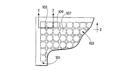
Conductive layer 103 is provided with a plurality of non-conductive areas 105,
such as
apertures or areas of non-conductive materials, conductive base areas 107 and
fuse links 109, for
example. The fuse links 109 connect base areas 107 each to the other.
The base areas, 107, can be large enough to function individually as
inefficient microwave
susceptors, but should not be so large as to function individually as
efficiently as a conventional
sheet susceptor. Alternatively, they can be too small to individually act as
microwave susceptors
and heat up significantly on exposure to microwave energy. However, a group of
such areas,
CA 02211071 1997-07-21
WO 96/34810 PCT/US96/05939
-5-
whether large or small, linked together by fuse links 109, converts microwave
energy into heat
overall similarly to a large conventional susceptor. As will be explained in
greater detail, below,
heat generation of such a susceptor including fuse links 109 is concentrated
to a greater or lesser
degree in the fuse links 109, depending upon the geometry of those fuse links
109. As will also
be explained in greater detail below, if one area (Fig. 3, 300a) of the
susceptor is over-exposed to
microwave energy, fuse links in that area will break, isolating that area from
other areas (Fig. 3,
300b) of the conductive structure. As a result, those areas (Fig. 3, 300a and
300b) will operate
less effectively as a microwave susceptor.
Failure of the fuse links is a function of the supporting substrate, the
thickness of the
conductive layer 103, the constituent material of the conductive layer, the
dimensions of the
pattern defining the fuse links 109 and the dimensions of the base areas 107
as well as variables
related to the food, the location of the food within the oven cavity and the
oven type.
Furthermore, fuse links may develop small cracks that permit displacement
currents to flow
through the cracks possibly in a capacitive coupling fashion, before failing
entirely. This, and
other factors, discussed below, permit the design of fast and slow fuses, and
high heating and low
heating fuses. Pattern dimensions and corresponding fuse link behavior is
presently determined
on an empirical basis. Fuse links covering an area of about 0.1 mm2 to 20 mmz
are suitable.
Hotter susceptors are possible using the present invention, because the sheet
resistance of a
susceptor constructed with fuses is higher than that of a susceptor
constructed of a similar
thickness layer of metal, but without fuses. The apertures through the metal
layer, which define
the fuse links 109 and base areas 107 are non-conductive. Therefore, current
flow is restricted to
the areas of the fuse links 109 and base areas 107. This restriction of
current flow is due to an
effectively higher sheet resistance. The sheet resistance of a susceptor is
also related to the
surface impedance of the susceptor at the frequencies of operation in
microwave ovens, and
power transfer from one transmission medium to another depends upon the
matching of the
impedances from one medium to another. The impedance of air is relatively high
at the
frequencies of interest. Therefore, by raising the sheet resistance of the
susceptor and
consequently raising the surface impedance, a better match to the air is
achieved. Thus, more
power is transferred into the susceptor, which converts the microwave energy
received into heat.
By orienting the fuses to avoid placement along the axis of greatest stretch
of the substrate, the
fuses may be set for a higher heat, without breaking, than would be achieved
by a conventional
susceptor, which would begin to break when the recoil forces began to rupture
the film.
CA 02211071 1997-07-21
WO 96/34810 PCT/US96/05939
-6-
Cooler susceptors are also possible using the present invention. Fuses break
when the
local temperature reaches the temperature at which the substrate recoil force
grows large enough
to break the fuse. The fuses may be set to break at relatively low susceptor
surface average
temperatures, thus limiting the overall heat generated by the susceptor
structure, by making the
fuses relatively small. A cooler susceptor may use relatively small base
areas, for example about
2 - 3 mm on a side, having a relatively heavy deposition of metal, for example
reaching an
optical density of about 0.45. In a conventional susceptor, such a thick layer
of metal would be
subject to relatively rapid, uncontrolled breakage, due to rapid heating from
high currents
generated. However, the fused susceptor according to the present invention
would break down in
a controlled fashion, at a controlled temperature. By using small, thick base
areas, the susceptor
could continue to operate at a lower efficiency, providing a low, but steady
heat to the food.
The present invention, when embodied as described above using a relatively
thick metal
layer, is advantageously used in a bag or wrap configuration, as shown
schematically in Fig. 8,
with the food 801 placed in the center. In such an application, the relatively
thick metal layer
reflects some of the microwave energy impinging on it 803. An additional
quantity of
microwave energy 805 is absorbed by the metal layer and converted to heat 807
which is
conducted to the food surface. A small remaining quantity of microwave energy
809 passes
through the metal layer to cook the interior of the food. Such operation is
particularly suitable
for food items which are susceptible to overcooking by microwave and which
require crisping or
browning at high temperature, such as filled pastries and some meats.
A number of patterns have been proposed. For example, the patterns shown in
Figs. 1 B
and 1 C will produce different degrees of heating of food articles and fuse
links, both before and
after fuse links break. The pattern of Fig. 1B may be characterized as having
slow, hot fuses
109, whereas the pattern of Fig. 1 C may be characterized as having fast, cool
fuses 109. This
difference in fuse behavior arises as follows.
Fuse links function as conventional fuses; that is, a fuse with a larger
conductive
cross-section than a second fuse requires greater current to fail than that
required to make the
second fuse to fail. With the same conductive layer thickness, wider fuse
links having
corresponding larger cross-sectional areas and connecting adjacent base areas,
fail at higher
temperatures than narrower fuse links due to increased current capacity. These
wider fuse links
also take longer to reach failure temperature. In Fig. 1B, the fuse is wider
than the distance
between opposite edges of the adjacent non-conductive area, resulting in a
slow, hot fuse. In
CA 02211071 1997-07-21
WO 96/34810 PCT/US96/05939
-7-
Fig. 1C, the fuse is narrower than the distance between opposite edges of the
adjacent
non-conductive area, resulting in a fast, cool fuse, because the current
carrying capacity of the
fuse is decreased. The fuse design rules discussed with respect to these
patterns are applied to
make fuse breakage uniform across the structure as described later.
In Fig. 3, the effect of irregularly shaped food articles on a conductive
structure according
to the present invention is seen. Food articles 301, shown in phantom, are
placed on a
conductive structure 303, in accordance with the present invention. Fuse links
305, 307 and 309
are exposed directly to microwave energy. Therefore, they break, isolating
portions 300a and
300b of the conductive structure 303 from one another. The microwave energy
absorbed in the
region near broken fuse links 305, 307, 309 and subsequently converted into
heat is reduced.
Fuse link 311, being partially covered by a food article 301 has partially
broken. Thus,
microwave heating of those areas of conductive structure 303 has been
partially reduced. Since
less microwave energy is absorbed by the regions of conductive structure 303
where fuses have
broken, the solid regions of conductive structure 303 under food articles 301
now absorb
relatively more microwave energy and produce more heat. Therefore, the
effectiveness of
conductive structure 303 in the areas covered by food articles 301 has been
enhanced.
In addition to the variables discussed above, failure of the fuse links is a
function of the
relationships between non-conductive areas 105, fuse links 109 and base areas
107 and the
polymeric substrate (Fig. 2, 101), as now discussed.
A biaxially oriented polyethylene terephthalate (PET) film is a polymeric film
which has
been stretched in two orthogonal directions. The two directions are usually
the machine
direction, i.e., the direction of film travel, and the across-the-web
direction, i.e., perpendicular to
the machine direction. Stretching a crystalline or partially crystalline film
and then rapidly
cooling or quenching the film imparts several beneficial physical
characteristics to the film such
as increased strength and yield (measured in square inches of film produced
per pound of raw
material). Typically the film is stretched more in one direction than the
other. However, if the
oriented film is brought above its orientation temperature, then it tends to
shrink to its former
size. Such films exhibit a greater recoiling or shrinkage force in the
direction of greater stretch
than in the other direction. The shrinkage is due to the stretched polymer
chains recoiling, much
like springs. Shrinkage can cause the PET film to rupture, and a small rupture
can propagate.
Ruptures and tears may disrupt susceptor operation by isolating some areas
from others, resulting
in uneven heating. In some cases, there may be excess heat build up in
localized regions.
CA 02211071 1997-07-21
WO 96/34810 PCT1US96/05939
-8-
Consider a fuse susceptor pattern, as shown in Figs. 1 A, 1 B or 1 C deposited
on a typical
biaxially oriented film with all fuses being the same size and shape, and with
fuses being aligned
with the film's directions of stretch. When exposed to microwave energy, the
fuses arranged
between base areas aligned in the direction of greatest stretch will break
before fuses aligned
with direction of lessor stretch, due to the difference in recoil force
generated upon heating.
However, the fuse links of a fuse susceptor pattern, shown in Fig. 5, having
its axes aligned 45o
to the machine and across-the-web directions will break at substantially the
same time, when
illuminated with approximately the same quantity of electromagnetic energy,
everything else
also being equal. Furthermore, since the recoil force exerted upon the fuses
aligned as described
is less than conventionally aligned fuses, otherwise equivalent fuses aligned
as described will
break at a somewhat higher temperatures.
Alternatively, in order to cause fuse links to break at substantially the same
time after the
same exposure to microwave energy, the fuse links could be aligned with the
machine and
across-the-web directions, as previously done, but with fuse links sized to
compensate for the
different shrinkage forces in the film as shown in Fig. 6. In Fig. 6, to
increase their current
carrying capacity, fuse links 601, aligned in the across-the-web direction are
wider than fuse
links 603, aligned in the machine direction.
Advantages of the present invention may include, but are not limited to,
greater heat flux
than current susceptors, safer, more uniform heating and achievement of both
lower temperature
and higher temperature conductive structures. By varying the fuse dimensions,
different heating
characteristics may be achieved. Small hot fuses may be made, which do not
rupture the PET
substrate, because they are not oriented on the weak axis of the substrate.
Conversely, large
cooler fuses which generate very uniform temperatures may be made, because the
break points of
fuses are made uniform by use of the invention. Aligning the fuse links at a
45o angle with the
film's orientation directions, as shown in Fig. 5, directs the current and
hence the heating away
from the weakest direction of the polymeric substrate, resulting in a more
robust fuse susceptor.
The fuse links begin to break at higher temperatures than similar dimension
fuses oriented with
the direction of greatest stretch.
The pattern of Fig. 7 includes these distinct regions, whose fuses and base
areas have
differing geometries. The center region is designed to have small base areas
701 and
proportionally large, hot fuses 703. Thus, the center region provides the
greatest heating effect to
the food. The fuses 703 of the center region provide a safety mechanism which
prevents
CA 02211071 1997-07-21
WO 96/34810 PCT/US96/05939
-9-
overheating of this hot region. The middle band has somewhat larger base areas
705 than the
center region, but the fuses 707 are a relatively smaller proportion of the
size of the base areas
705 than in the center region. These design choices provide somewhat less heat
than the center
region, because the fuses 707 break at a lower temperature than fuses 703, but
the base areas 705
nevertheless remain operative at a reduced efficiency after fuses 707 break.
In the outer region
are found the largest base areas 709 and the proportionally smallest fuses
711. As a result, the
outer region provides the lowest heat generation. When the fuses 711 break,
which here occurs
at the lowest temperature, the base areas 709 operate as susceptors, but at a
reduced efficiency.
Thus, this design directs the greatest heat to the food region, while the
edges remain somewhat
cooler.
The material described in connection with Fig. 7 is particularly suitable for
cooking foods
like pizza, when made as described in connection with Fig. 8. Where food is in
proximity with
the susceptor material, the fuses tend not to break, but to continue to
produce heat. Thus, the
middle part of the pizza dough may be crisped, without burning the edges.
Conductive structures in accordance with the present invention may be made by
a variety
of methods known to those skilled in the art. In general, any method which can
produce a thin
pattern film of metal on a plastic substrate is suitable. For example, pattern
printing and etching
techniques are suitable. Another such method is now described in connection
with Fig. 4.
In accordance with this method, there is supplied from a supply reel 401 a
continuous web
of plastic substrate 403. The plastic substrate 403 is passed between rollers
405 and 407 which
cause to be printed on a bottom surface thereof a negative image in oil of the
desired pattern.
The plastic substrate 403 then passes above an aluminum deposition apparatus
409. The pattern
of oil printed by rollers 405 and 407 locally prevents deposition of metal.
Metal is, however,
deposited to regions not covered by the oil. Thus, take-up reel 411 receives a
substrate on which
a conductive structure film has been deposited having, for example, one of the
patterns shown in
Figs. lA-1 C.
Another example of a method for producing conductive structures according to
the present
invention is to deposit a uniform film of metal on a substrate and
subsequently etch metal away
to form the pattern required.
The present invention has now been described in connection with a number of
specific
embodiments thereof. However, numerous modifications which are contemplated as
falling
within the scope of the present invention should now be apparent to those
skilled in the art.
CA 02211071 1997-07-21
WO 96/34810 PCT/US96/05939
-10-
Therefore, it is intended that the scope of the present invention be limited
only by the scope of
the claims appended hereto.