Note: Descriptions are shown in the official language in which they were submitted.
CA 02211197 1997-07-23
W 096126556 PCTAUS96/02516
UT~U FP~O~N~ MOnUr~ pr.~G ~nn ~RT-~ ~S~MRr.Y
R~r-~ylGl~d of the Tnvpn~-ion
This invention relates generally to electrical
connector and cable assemblies and, more particularly, to
an assembly of a multi-pair cable terminated by a modular
plug for use in the transmission of high frequency
signals.
Data communication networks are being developed
which enable the flow of information to ever greater
numbers of users at ever higher transmission rates. A
problem is created, however, when data is transmitted at
high rates over a plurality of circuits of the type that
comprise multi-pair data communication cable. In
particular, at high transmission rates, each wiring
circuit itself both transmits and receives
electromagnetic radiation so that the signals flowing
through one circuit or wire pair (the "source circuit")
may couple with the signals flowing through another wire
pair (the "victim circuit"). The unintended
electromagnetic coupling of signals between different
pairs of conductors of different electrical circuits is
called crosstalk and is a source of interference that
often adversely affects the processing of these signals.
The problem of crosstalk in information networks
CA 02211197 1997-07-23
W 096/26556 PCTrUS96/02516
increases as the frequency of the transmitted signals
increases.
In the case of local area network (LAN) systems
employing electrically distinct twisted wire pairs,
crosstalk occurs when signal energy inadvertently
"crosses" from one signal pair to another. The point at
which the signal crosses or couples from one set of wires
to another may be 1) within the connector or internal
circuitry of the transmitting station, referred to as
"near-end crosstalk", 2) within the connector or internal
circuitry of the receiving station, referred to as "far-
end crosstalk", or 3) within the interconnecting cable.
Near-end crosstalk ("NEXT") is especially
troublesome in the case of telecommunication connectors
of the type specified in sub-part F of FCC part 68.500,
commonly referred to as modular connectors. Such modular
connectors include modular plugs and modular jacks. The
EIA/TIA (Electronic/Telecommunication Industry
Association) of ANSI has promulgated electrical
specifications for near-end crosstalk isolation in
network connectors to ensure that the connectors
themselves do not compromise the overall performance of
the unshielded twisted pair interconnect hardware
typically used in LAN systems. The EIA/TIA Category 5
electrical specifications specify the minimum near-end
crosstalk isolation for connectors used in lO0 ohm
CA 02211197 1997-07-23
W 096/26556 PCT~US96/02516
unshielded twisted pair Ethernet type interconnects at
speeds of up to 100 MHz.
A high speed data transmission cable is typically
terminated by a modular plug which conventionally
comprises an insulating housing in which a planar array
of closely spaced parallel passages receive the ends of
respective cable wires. The cable typically comprises
four circuits defined by eight wires arranged in four
twisted pairs and is typically terminated by modular plug
having eight contacts engaging the ends of the eight
wires, which are received in respective wire-receiving
passages arranged in a row. Specified ones of the four
pairs of the plug contacts are assigned to terminate
respective specified ones of the four cable wire pairs
according to ANSI/EIA/TIA st~n~rd 568. For example, the
standard 568 contact assignment for the wire pair
designated #l are the pair of plug contacts located at
the 4-5 contact positions. The cable wires of the pair
designated #3 are, according to standard 568, terminated
by the plug contacts located at the 3-6 positions which
straddle the 4-5 plug contacts that terminate wire pair
#1. Near-end crosstalk between wire pairs #1 and #3
during high speed data transmission has been found to be
- particularly troublesome in modular plugs that terminate
cable according to standard 568.
CA 022lll97 l997-07-23
W 096/26556 PCTrUS96/02516
5~La~ry of ~-he TnvQnt;on
Accordingly, an object of the present invention is
to provide a new and improved cable and connector
assembly.
Another object of the present invention is to
10provide a new and improved modular plug and cable
assembly.
Still another object of the present invention is to
provide a new and improved modular plug and multi-pair
cable assembly for use in the transmission of high
15frequency signals which provides a significant reduction
in near-end crosstalk compared to conventional apparatus.
The present invention is based on the recognition
that in a modular plug terminating a multi-pair cable,
20crosstalk between two pairs of conductors defining
different circuits, i.e. between two "signal pairs",
results from both magnetic field (inductive) and electric
field (capacitive) coupling and that the magnitude of
such coupling between the two signal pairs can be reduced
25by suitably positioning the ends of the signal pairs in
the plug and adjusting the spacing between them.
Briefly, as to magnetic field coupling, in
accordance with the invention, a modular plug is
constructed and the four ends of the two signal pairs are
30positioned and fixed in the plug such that the signal
CA 02211197 1997-07-23
W 096/26556 PCTAUS96/02516
pins generate signal loops that are oriented at an angle
to each other, preferably approaching a right angle. The
magnetic field coupling and crosstalk induced between the
two signal pairs is thereby reduced compared to the
conventional plug construction which requires the signal
pins to be positioned in a single row or planar array so
that their signal loops are co-planar. A s t o
electric field coupling, a modular plug according to the
invention is constructed to enable the spacing between
the signal pins of the signal pairs under consideration
to be more evenly balanced. Since the magnitude of the
pin-to-pin capacitance is determined solely by the
distance between the two signal pins under consideration,
the electric field or capacitive coupling and crosstalk
induced between the two signal pairs is reduced compared
to the conventional plug construction in which the pin-
to-pin spacing is less symmetrical.
In a preferred embodiment of the invention, a
modular plug includes an insulating or dielectric housing
having a plurality of wire-receiving passages disposed in
first and second substantially parallel planar arrays
spaced one above the other, the passages of the first
planar array being staggered in position with respect to
~ the passages of the second planar array. The end of a
first wire of each of the first and second wire or signal
pairs is received in a respective wire-receiving passage
=
CA 02211197 1997-07-23
W 096/26S56 PCT~US96/02S16
in the first planar array while the end of a second wire
of each of the first and second signal pairs is received
in a respective wire-receiving passage in the second
planar array. The wire-receiving passages in which the
wire ends of the first and second wire pairs are received
are selected such that the pins of the first signal pair
are situated in a first pair plane and the pins of the
second signal pair are situated in a second pair plane
that intersects the first pair plane, so that the signal
loops generated by the signal pairs are oriented at an
angle to each other.
The ends of the first signal pair are preferably
received in adjacent wire-receiving passages of the first
planar array while the ends of the second signal pair
received in adjacent wire-receiving passages of the
second plane or array contiguous with the two adjacent
wire-receiving passages of the first planar array, i.e.,
one of the passages receiving a respective one of the
second wire ends is situated intermediate of the pair of
passages receiving the first wire ends. This results in
the two pair planes, and therefore the signal loops,
being oriented at a substantially right angle to each
other minimizing magnetic field coupling and additionally
more closely balances the pin-to-pin spacing, and
therefore the pin-to-pin capacitances, thereby reducing
electric field coupling and capacitively coupled
CA 02211197 1997-07-23
W096/26ss6 PCT~S96/02516
crosstalk.
In a preferred embodiment, the modular plug has
eight wire receiving passages and the multiconductor
cable includes four signal pairs. The first and second
planar arrays each include four of the wire receiving
passages, viz., two outer passages and two inner
passages. The ends of first wires of two of the wire
pairs are received in the two inner passages of the first
planar array and the ends of the second wires of the two
wire pairs are received in the two inner passages of the
second planar array to form intersecting pair planes.
Descript;on of the Draw;ngs
A more complete appreciation of the present
invention and many of the attendant advantages thereof
will be readily understood by reference to the following
detailed description when considered in connection with
the accompanying drawings in which:
Fig. l is a perspective view of a conventional
modular plug and multi-pa1r cable prior to termination
according to the prior art;
Fig. 2 is a transverse cross-section view of the
prior art modular plug and cable assembly shown in Fig.
- l taken along line 2-2 of Fig. l;
Fig. 3 is a schematic illustration of the transverse
cross-section of the conventional plug receiving the
-
CA 02211197 1997-07-23
W 096/26556 PCTrUS96/02516
cable wires corresponding to Fig. 2 and showing the
stAn~Ard terminal assignments for signal pairs #1 and #3;
Fig. 4 is a schematic illustration of the
orientation of the signal loops generated by the signal
pairs #1 and #3 of Fig. 1 in the conventional
construction;
Fig. 5 is a schematic illustration similar to Fig.
3 of the transverse cross-section of a plug receiving
cable wires in accordance with the present invention and
showing the standard terminal assignments for signal
pairs #1 and #3;
Fig. 6 is a transverse cross-section view similar to
Fig. 2 of a modular plug and cable assembly in accordance
with the present invention;
Fig. 7 is a schematic illustration similar to Fig.
4 of the orientation of the signal loops generated by the
signal pairs #l and #3 of the assembly of FigO 5 and 6 in
accordance with the invention;
Fig. 8 is a bridge circuit representation
schematically illustrating pin-to-pin capacitive coupling
between signal pairs #1 and #3 for both the prior art
modular plug of Fig. 1 and a modular plug according to
the invention of Fig. 3;
Fig. 9 is a voltage divider representation
schematically illustrating pin-to-pin capacitive coupling
between signal pairs #1 and #3 for both the prior art
CA 02211197 1997-07-23
W O 96/26556 PCTAUS96/02516
modular plug of Fig.1 and the modular plug according to
the invention of Fig. 3;
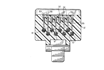
Fig. 10 is a perspective view similar to Fig. 1 of
a modular plug and cable assembly in accordance with the
present invention prior to connection;
Fig. 11 is a top plan view of the connector-cable
assembly of Fig.10 in accordance with the invention; and
Fig. 12 is a longitudinal section view of the
connector-cable assembly taken
along line 12-12 of Fig. 11.
Description Of The Preferred ~mbodiment
Referring now to the drawings wherein like reference
characters designate identical or corresponding parts
throughout the several views, the reduction in crosstalk
achieved by the invention will initially be described
with reference to Figs. 1-7.
Referring to Figs. 1 and 2, a conventional modular
plug 10 for terminating a multi-pair communication cable
14 is illustrated. Cable 14 comprises an insulating
sheath 16 enclosing four pairs of conductors or wires 18,
each wire pair or signal pair forming a separate signal
circuit during use. The construction of plug 10 is well
known and generally comprises a dielectric housing 20
having a closed forward free end 22, a cable-receiving
rearward end 24, a terminal receiving side 26 and a
CA 02211197 1997-07-23
W 096/26556 PCTrUS96/02516
cable-receiving cavity (not shown) exten~;ng
longitl~;n~lly from the rearward end 24 of housing 20 to
a front end. Eight parallel slots 28 defined by
corresponding fins 29 open on to the terminal-receiving
side 26 of housing 20 for receiving flat contact
terminals 30. The eight slots 28 are aligned over a
planar array of respective longitu~;n~lly extending
parallel passages 32 which communicate with the cable-
receiving cavity and which receive the ends of respective
cable wires 18. Each flat contact terminal 30 is
inserted into and fixed within an associated terminal-
receiving slot 28 to terminate a respective wire 18
located in a respective wire-receiving passage 32.
A noted above, near-end crosstalk between signal
pairs #l and #3 during high speed data transmission has
been the most troublesome in modular plugs that terminate
cable according to standard 568. Referring to Fig. 3, a
schematic illustration similar to Fig. 2 of the
transverse cross-section of plug 10 receiving the ends of
cable wires 18 shows the conventional planar array of
passages 32 in which the wires 18 are inserted,
designated by position numbers 1 to 8, and the standard
terminal arrangement for signal pairs #l and #3. As
shown in Fig. 3, the ends of wires 18 of signal pair #1
are received in passages 4 and 5 and the wires 18 of
signal pair #3 are received in passages designated 3 and
.
CA 02211197 1997-07-23
W 096/26556 PCTrUS96/02516
6 which straddle the 4-5 passages that receive the ends
of the wires of signal pair 1.
It has been recognized that as schematically
illustrated in Fig. 4, with the ends of signal pairs #1
and #3 in the conventional arrangement of wire passages
32 according to the s~An~Ard, the signal loop defined by
signal pair #1 has an orientation that is co-planar with
and which resides entirely within the signal loop defined
by signal pair #3 and that such an arrangement maximizes
the magnetic field coupling and the resultant crosstalk
between these two signal pairs.
Reference will now be made to Figs. 5-7 in which
parts corresponding to parts shown in Figs. 1-4 are
designated by the same reference numerals, primed. In
accordance with the invention, in order to reduce the
magnetic field coupling and crosstalk induced between two
signal pairs, the passages 32' are arranged in a manner
such that the signal loops defined by signal pairs #l and
#3 are oriented to occupy pair planes that intersect each
other. Specifically, as shown in Figs. 5 and 6, wire-
receiving passages 32' are disposed in first and second
substantially parallel planar arrays of four passages
each, spaced one above the other, with the passages of
the planar arrays being staggered in position with
respect to each other.
The cable wires 18' are inserted into passages 32'
CA 02211197 1997-07-23
W 096/26556 PCTrUS96/02516
in accordance with the st~n~rd terminal arrangement for
signal pairs. Thus, the ends of first wires 18' of
signal pairs #l and #3 are inserted into passages 32' at
inner, now laterally adjacent, positions 4 and 6 of the
first upper planar array and the ends of the other wires
of pairs #1 and #3 are inserted into passages 32' at
inner, now laterally adjacent, positions 3 and 5 of the
second lower planar array. The pair of upper array
passage positions 4, 6 can be said to be "contiguous" to
the pair of lower array passage positions 3, 5 since
lower position 5 is situated laterally intermediate of
upper positions 4, 6. In this standard configuration,
the wire ends of signal pairs #l and #3 form parts of
signal loops that lie in pair planes that intersect each
other at a point "a" situated between the planes of the
first and second planar arrays of passages 32'. Indeed,
as schematically shown in Fig. 7, the signal loops lie in
pair planes that intersect each other at a substantial
right angle, the particular orientation at which magnetic
field coupling and crosstalk induced between the two
signal pairs is r;n;m;zed. Although crosstalk resulting
from magnetic field coupling is minimized when the pair
planes form a substantial right angle with each other, or
at least intersect at a point between the planes of the
two planar arrays, it will be understood that benefits in
accordance with the invention will be obtained so long as
CA 02211197 1997-07-23
W 096/26556 PCTAUS96/02516
S the pair planes intersect at some point. This is assured
when, with the modular plug oriented such that the first
and second planar arrays of wire receiving passages are
substantially horizontal, the first pair plane extends
upwardly and in one lateral direction while the second
pair plane extends upward and in the other lateral
direction.
It will also be understood that the present
invention does not merely comprise providing a modular
plug with a dual array of staggered wire-receiving
passages per se. Indeed, such construction per se is
shown in the prior art, viz. U.S. 4,054,350. Rather, the
invention comprises a combination multi-pair cable and
plug assembly wherein the wire ends of two signal pairs
are positioned and fixed within the modular plug as
described above to reduce magnetic field coupling and
crosstalk induced between the two pairs. To applicants'
knowledge, this invention is neither taught nor suggested
by the prior art.
As noted above, crosstalk in a modular plug also
results from electric field or capacitive coupling. In
accordance, with the invention, it has been recognized
that the magnitude of such coupling between two signal
pairs is determined by the degree of symmetry of the
distances between the ends of the four wires of those
pairs. To simplify the following discussion relating to
CA 02211197 1997-07-23
W 096/26S56 PCTrUS96/02S16
capacitive coupling, those terminated wire ends of the
two signal pairs are referred to as "pins", and the pins
of signal pairs #1 and #3 located according to the
st~n~rd terminal arrangement in wire passages at
positions 4, 5 and 3, 6 respectively, are referred to as
pin 4, pin 5, pin 3, and pin 6 respectively.
Fig. 8 illustrates the dominant pin-to-pin
capacitances that exist within both a conventional
modular plug as well as in a modular plug constructed in
accordance with the invention. The capacitance between
pin 3 and pin 6 has been neglected in order to simplify
the model. The diamond shaped arrangement shown is often
used to represent a balanced bridge type circuit. To
illustrate the generation of crosstalk within the plug,
a signal source Vsig is applied to signal pair number 3 at
pin 3 and pin 6.
The magnitude of undesirable capacitive coupling
between signal pairs can be estimated by the magnitudes
of the capacitances in relation to one another. Since
all the pins are identical and parallel, the magnitude of
each pin-to-pin capacitance will depend entirely upon the
distance between the two pins under consideration. If
all pin-to-pin capacitances were equal and the four
signal pins corresponding to signal pairs #1 and #3 were
arranged in a symmetrical (with identical spacing between
nodes) diamond, a near zero capacitive coupling between
CA 02211197 1997-07-23
W 096/26556 PCTAUS96/02516
the two pairs would be expected. Such an arrangement
will maintain electrical balance of signal pairs, where
each signal pin "sees" the same impedance between itself
and every other conductor in the system.
The maintenance of an electrical balance between
signal pairs where each signal pin sees the same
impP~nce between itself and every other conductor in the
system can be explained by using a voltage divider model
shown in Fig. 9. The capacitively induced crosstalk
voltage VcrOsstalk~ will be zero if the circuit is perfectly
balanced, i.e., if the voltages at pin 5 and pin 6 are
made to sum to zero. Viewing each of the two arms of the
circuit as a voltage divider, the circuit will be
balanced if.
[1] lcs-6l- lc4
lc3-sl+lcs-6l lc3 4l+lc4-6l
As noted above, the magnitude of the pin-to-pin
capacitances will be determined by the spacing between
the pins. The capacitive balance of the standard single
row modular plug can be compared to the balance of a
dual, staggered row modular plug in accordance with the
invention by replacing the subscripts of the pin-to-pin
capacitances in formula [1] with the actual pin spacing.
A 0.04 inch center-to-center adjacent pin spacing and
0.035 inch center-to-center row height spacing has been
chosen, and the equations for a single row conventional
CA 02211197 1997-07-23
W096/26556 PCTtUS96tO2516
modular plug and a dual, staggered row modular plug in
accordance with the invention are set forth below in
equations 2 and 3 respectively.
t2] lc4o! lC80l
lc80l+1cqOl lc40l+
[3] ICs31 1C80
lc8Ol+lc53l 1c~3l+lc8ol
It is noted that the denominators in equations 2 and
3 are equal and that C80 is the right hand side numerator
for both expressions. The modular plug according to the
invention clearly achieves better balance since Cs3 is
s closer in value to C80 than is40C . The decibel
improvement in balance can be represented by:
= 2OLog [change in capacitance relative to change
for perfect balance]
= 20Log 53-40
= 2.44 dB.
Referring to Figs. 6 and 10, two sets of contact
terminals are required to terminate the wires 18', viz.
a set of four shorter terminals 30a and a set of four
longer terminals 3Ob. The longer contact terminals are
situated in respective slots and pass between adjacent
wire passages in the first upper planar array to
terminate the wire ends received in the wire passages of
the second lower planar array.
Referring to Fig. 10-12 a load or management bar 34
CA 02211197 1997-07-23
W 096/26556 PCTrUS96/02516
is utilized to facilitate aligning the wire ends with
their corresponding wire-receiving passages 32' during
the cable insertion step of termination. Management bar
34 comprises a block-shaped plastic member having an
outer configuration which corr~cron~-c to the shape of the
forward end of the cable-receiving cavity 36 (Fig. 12).
A pair of planar arrays of four bores 38 each are formed
through bar 34 having the same spacing as the dual array
arrangement of wire-receiving passages 3 2'. The diameter
of each of the bores 38 iS slightly larger than the
diameter of the wires 18' to allow for a sliding fit of
the wires 18' in bores 38. In assembly, the wires 18' of
the four signal pairs are initially inserted into the
particular bores 38 of management bar 34 that correspond
in location to the positions of passages 32~ designated
by the standard terminal arrangement. The lengths of the
wires 181 that protrude beyond the forward face 40 of bar
34 are sheared flush with the forward face 40 whereupon
the wire-carrying bar is inserted into the cable-
receiving cavity 36 of plug 10'. The bar is urged
forwardly through cavity 36 until its forward face 40
abuts the front end of cavity 36 as seen in Fig. 12. The
cable wires are then urged forwardly through bores 38 and
pass into the aligned wire-receiving passages 32'. It is
understood that the management bar may have other
configurations such, for example, as one in which the
CA 02211197 1997-07-23
W O 96/26556 PCTrUS96/02516
bores of the upper array are replaced by a planar array
of channels that open onto the top surface 42 of bar 34
to facilitate insertion of the wires thereunto.
Obviously, numerous modifications and variations of the
present invention are possible in the light of the above
teachings. It is therefore to be understood that within
the scope of the claims appended hereto, the invention
may be practiced otherwise than as specifically disclosed
herein.