Note: Descriptions are shown in the official language in which they were submitted.
CA 02211238 1997-07-23
220/202
PATENT
S P E C I F I C A T I O N
TITLE OF THE INVENTION
INKJET PRINT HEAD APPARATUS
Backqround of the Invention
1. Field of the Invention
The present invention pertains to the field of inkjet
printers, and more specifically, to piezoelectric inkjet print
heads.
2. Description of Related Art
Ink jet printers, and more particularly, drop-on-demand
-inkjet print heads having a piezoelectric transducer actuated by
electrical signals, are known in the art. Typical print heads
~5 consist of a transducer mechanically coupled to an ink chamber,
wherein the application of an electrical signal to the transducer
material causes the transducer to deform in shape or dimension
within or into the ink chamber, thereby resulting in the
expulsion of ink from an ink chamber orifice. One disadvantage
of prior art print head structures is that they are relatively
large in overall dimension, and thus cannot be placed together
into a densely packed array; this reduces available output dot
density, which will decrease the overall output definition of a
printer. Another disadvantage with prior art devices is that the
large number of components in these devices tend to increase the
costs and difficulty of manufacture. Further, the prior art
CA 02211238 1997-07-23
220/202
PATENT
structures, when placed next to each other within an array to
create a multi-channel print head, tend to produce undesirable
"crosstalk" between adjacent ink chambers, which interferes with
the accurate ejection of ink from the print head.
Therefore, there is a need in the art for a print head
structure which can be advantageously and economically
manufactured, but can also be placed in a densely packed array of
such structures for a multiple-channel print head for increased
output dot density. Further, there is a need for a multi-channel
print head structure which minimizes undesirable crosstalk
effects.
- Summarv of the Invention
The present invention comprises an inkjet print head
wherein the placement of the transducer electrodes in combination
with the particular poling direction (overall polarization
direction) of the print head transducer material provides for an
efficient combination of shear and normal mode actuation of the
print head. According to one embodiment of the invention, a
print head transducer is defined by a first wall portion, a
second wall portion, and a base portion, in which the interior
walls of these wall and base portions form three sides of an ink
channel. The upper surfaces of the wall portions define a first
face of the print head transducer, and the lower surface of the
base portion defines a second, opposite face of the transducer.
A metallization layer, forming a common electrode, is deposited
CA 02211238 1997-07-23
220/202
PATENT
on the interior surfaces of the ink channel and along the upper
surfaces of the first and second wall portions. A second
metallization layer, forming the addressable electrode, is
deposited on the entire outer surface of the base portion, and on
a portion of the outer surfaces of the first and second wall
portions. The poling direction of the piezoelectric material
~ forming the print head transducer is substantially perpendicular
to the electric field direction between the addressable
electrodes and the common electrode at the first and second wall
portions, providing fo~ shear mode deflection of the wall
portions, toward or away from each other, upon the application of
an electrical drive signal to the addressable electrodes. The
-poling direction of the piezoelectric material forming the print
head transducer is substantially parallel to the electric field
direction between the addressable electrodes and the common
electrode at the center of the base portion, providing for normal
mode actuation of the center of the base portion when an
electrical drive signal is applied. The metallization layer
forming the addressable electrodes preferably extends halfway
along the height of the wall portions. The metallization layer
forming the common electrode is preferably maintained at ground
potential.
The present invention also comprises a plurality of ink
ejecting structures capable of being densely packed into a linear
array of multiple ink channels. This array comprises a
transducer formed from a sheet, wafer or block of piezoelectric
CA 02211238 1997-07-23
220/202
PATENT
material, into which a series of ink channels are cut into a
first face of the piezoelectric sheet material. A second
opposite face of the piezoelectric sheet contains a series of air
channels, each of which are interspaced between each of the ink
channels. A metallization layer forming the common electrode is
coated over the first face of the sheet and on the interior
surface of each ink channel. A second metallization layer
forming the addressable electrodes is coated over the second face
and on the interior surface of each air channel, with the second
metallization layer initially connected from air channel to air
channel. An electrode-separation channel is cut into the bottom
of each air channel, which breaks the connection of the second
- metallization layer between adjacent air channels, and which also
extends the gap depth within the combined air/electrode-
separation channels further toward the first face of thepiezoelectric block. This transducer structure for an array of
ink channels is particularly advantageous in that it provides for
minimal mechanical crosstalk between adjacent ink channels. An
alternate embodiment further minimizes crosstalk, by feeding ink
from an ink reservoir to the ink channels via one or more slotted
ink passages, which serve to reduce the transfer of pressure
waves from one ink channel to another.
These and other aspects of the present invention are
described more fully in following specification and illustrated
in the accompanying drawing figures.
CA 02211238 1997-07-23
220/202
PATENT
Brief Descri~tion of the Drawinas
Fig. 1 is a cross-sectional side view of an inkjet print
head structure for a single ink channel according to an
embodiment of the invention.
Fig. 2 iS a partial perspective view of the inkjet print
head structure of Fig. 1.
Fig. 3A is a front view of a portion of the structure of a
sheet of transducer material for an array of ink channels
according to the embodiment of the present invention shown in
Fig. 2.
Fig. 3B is a perspective view of the sheet of transducer
material shown in Fig. 3A.
- Figs. 4A-B illustrate the normal mode actuation of a block
of piezoelectric material.
Figs. 5A-B illustrate the shear mode actuation of a block
of piezoelectric material.
Fig. 6 is a partial diagram of the preferred print head
transducer structure showing electric fields established therein.
Figs. 7 and 8 illustrate the mechanical movement of the
transducer in the preferred print head structure constructed in
accordance with the present invention.
Fig. 9 depicts an alternate print head structure
constructed in accordance with the present invention.
Fig. 10 depicts an ink feed structure for an embodiment of
the present invention.
Fig. 11 shows the front view of an alternate print head
CA 022ll238 l997-07-23
220/202
PATENT
transducer structure according to the present invention, wherein
the addressable electrode metallization layer is not
symmetrically coated on the first and second wall portions.
Fig. 12 depicts the front view of a print head transducer
according to an alternate embodiment of the present invention.
DESCRIPTION OF THE PREFERRED EMBODIMENT
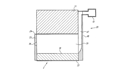
Fig. 1 is a cross-sectional side view of a single channel
of an inkjet print head structure 20 for a piezoelectric inkjet
printer constructed in accordance with an embodiment of the
present invention. Print head structure 20 comprises a print
head transducer 2, formed of a piezoelectric material, into which
is cut an ink channel 29. The ink channel 29 iS bordered along
one end with a nozzle plate 33 having an orifice 38 defined
therethrough. A rear cover plate 4 8 iS suitably secured to the
other end of ink channel 29. A base portion 36 of the print head
transducer 2 forms the floor of the ink channel 29, while an ink
channel cover 31 iS secured to the upper opening of the print
head transducer 2. Ink channel 29 iS supplied with ink from an
ink reservoir 10 through ink feed passage 47 in rear cover plate
48. As explained in more detail below, the actuation of the
print head transducer 2 results in the expulsion of ink drops
from ink channel 29 though the orifice 38 in nozzle plate 33.
Referring to Fig. 2, the print head transducer 2 of Fig. 1
iS shown in greater detail. The preferred print head transducer
2 comprises a first wall portion 32, a second wall portion 34,
CA 02211238 1997-07-23
220/202
PATENT
and a base portion 36. The upper surfaces of the first and
second wall portions 32 and 34 define a first face 7 of the
printed head transducer 2, and the lower surface of the base
portion 36 defines a second, opposite face 9 of the print head
transducer 2. Ink channel 29 iS defined on three sides by the
inner surface of the base portion 36 and the inner wall surfaces
of the wall portions 32 and 34, and is an elongated channel cut
into the piezoelectric material of the print head transducer 2,
leaving a lengthwise opening along the upper first face 7 of the
print head transducer 2. As described above, one end of ink
channel 29 iS closed off by an nozzle plate 33 (Fig. 1) while the
other end is closed off by a rear cover plate 48 (plates 33 and
- 48 are not shown in Fig. 2). A metallization layer 24 coats the
inner surfaces of ink channel 29 and is also deposited along the
upper surfaces of the first wall portion 32 and second wall
portion 34. An ink channel cover 31 is bonded over the first
face 7 of the print head transducer 2, to close off the
lengthwise lateral opening in the ink channel 29. A second
metallization layer 22 coats the outer surfaces of the base
portion 36, and also extends approximately halfway up each of the
outer surfaces of the first and second wall portions 32 and 34.
The metallization layer 22 defines an addressable
electrode 60, which is connected to an external signal source to
provide electrical drive signals to actuate the piezoelectric
material of print head transducer 2. In the preferred
embodiment, the metallization layer 24 defines a common electrode
CA 02211238 1997-07-23
220/202
PATENT
62 which is maintained at ground potential. Alternatively, the
common electrode 62 may also be connected to an external voltage
source to receive electrical drive signals. However, it is
particularly advantageous to maintain the common electrode 62 at
ground potential since the metallization layer 24 is in contact
with the ink within ink channel 29. Having the common electrode
at ground minimizes possible electrolysis effects upon the common
electrode 62 and the ink within ink channel 29, which may degrade
the performance and structure of both the common electrode 62
and/or the ink.
The preferred piezoelectric material forming the print
head transducer 2 is PZT, although other piezoelectric materials
-may also be employed in the present invention. The overall
polarization vector direction ("poling direction") of print head
transducer 2 lies substantially in the direction shown by the
arrow 30 in Fig. 2, extending in a perpendicular direction from
the second face 9 to the first face 7 of the print head
transducer 2. The print head transducer 2 may have other poling
directions within the scope of the present invention, including,
but not limited to, a poling direction which lies substantially
opposite (approximately 180 degrees) to the direction indicated
by the arrow 30 in Fig 2.
In the preferred embodiment, print head transducer 2 is
preferably formed from a single piece of piezoelectric material,
rather than an assembly of separate components which are secured
together into the desired structure (i.e., where the respective
CA 02211238 1997-07-23
220/202
PATENT
wall portions are distinct components which are bonded or glued
to a separate base portion). By forming the entire print head
transducer 2 from a single piece of piezoelectric material, the
deflection capability of the print head transducer 2 is thus not
limited by the strength or stiffness of glue lines or joints
between different transducer components.
In operation, the present invention works upon the
principle of the piezoelectric effect, where the application of
an electrical signal across certain faces of piezoelectric
materials produces a corresponding mechanical distortion or
strain in that material. In general, and of particular
importance to the present invention, the mechanical reaction of a
piezoelectric material to an electrical signal is heavily
dependent upon the poling direction of the piezoelectric
material, as well as the orientation of the applied electrical
field to that piezoelectric material.
Figs. 4A and 4B depict the normal mode actuation of a
typical piezoelectric material. In Fig. 4A, the piezoelectric
material 72 has a poling direction as indicated by arrow 70. A
voltage source 74 is connected across two exterior faces of
piezoelectric material 72, with the voltage source 74 applying an
electric field parallel to the poling direction 70 of the
material 72. As shown in Fig. 4B, this electric field causes a
normal mode mechanical distortion of the piezoelectric material
72, wherein one polarity of the applied voltage will cause
material 72 to elongate, becoming longer and thinner parallel to
CA 02211238 1997-07-23
220/202
PATENT
the poling direction 70 of the piezoelectric material 72. The
application of an opposite polarity voltage will cause material
72 to compress, becoming shorter and thicker, also parallel to
the poling direction 70 of the piezoelectric material 72 (as
shown in dashed lines in Fig. 4B).
Figs. 5A and 5B depict the shear mode actuation of a
typical piezoelectric material 76. In Fig. 5A, the piezoelectric
material 76 has a poling direction as indicated by arrow 78.
This time, however, the voltage source 74 iS connected across the
0 piezoelectric material 76 such that the application of voltage by
the voltage source 74 creates an electric field which runs
perpendicular to the poling direction of the piezoelectric
-material 76. As shown in Fig. 5b, this electric field causes a
shear mode mechanical distortion of the piezoelectric material
76, which causes material 76 to generally react by deflecting
towards a parallelogram shape, rather than the elongated or
compressed reaction of the normal mode. Depending upon the
manner in which material 76 iS restrained or held by an external
force, the material 76 may deform in a bending or twisting
manner. The particular direction, type of movement, and field of
movement for this mechanical distortion is dictated in part by
the shape, dimensions and/or composition of the piezoelectric
material 76, and also by the amplitude, polarity or frequency of
the electrical signal which is applied to the material 76. In
general, an applied voltage of one polarity will cause material
76 to bend in a first direction, and an applied voltage of the
CA 02211238 1997-07-23
220/202
PATENT
opposite polarity will cause material 76 to bend in a second
direction opposite that of the first.
Fig. 6 is a front view of one-half of the piezoelectric
material for the preferred single channel print head transducer 2
(i.e., one wall portion and one-half of the base portion). As
stated above, metallization layer 24 iS deposited on the interior
surfaces of ink channel 29 and on the upper surface of the wall
portion 34 to form the common electrode 62, which is preferably
maintained at ground potential. Metallization layer 22 iS coated
over approximately half the outer surface of wall portion 34 and
over the lower outer surface of base portion 36 to define an
addressable electrode 60, which is selectively connected to an
-electrical signal source to drive the print head transducer 2.
Upon the application of a positive voltage signal to the
addressable electrode 60, the orientation of the applied electric
field established in the transducer material is substantially as
shown in Fig. 6. At the center of the base portion 36 of the
print head transducer 2, it can be seen that a substantial
portion of the electric field generated between addressable
electrode 60 and common electrode 62 iS in the same direction as
the poling direction 30 of piezoelectric material, thereby
substantially actuating that portion of the transducer material
in the normal mode. At the wall portion 34, a substantial
portion of the electric field generated between addressable
electrode 60 and common electrode 62 iS perpendicular to the
poling direction 30, thereby substantially actuating that portion
- 11
CA 022ll238 l997-07-23
220/202
PATENT
of the transducer in the shear mode toward the other lateral wall
32 (see Fig. 7). In the preferred embodiment, the electric field
established between addressable electrode 60 and common electrode
62 changes in orientation, from the base portion 36 to the wall
portion 34, substantially as shown in Fig. 6.
Fig. 7 illustrates the movement of the transducer material
in the preferred embodiment upon application of a positive
voltage to the addressable electrode 60. The dashed lines in
Fig. 7 indicate the directional extent of movement by the print
head transducer 2 upon the application of a positive voltage.
Since the material of base portion 36 iS substantially actuated
in the normal mode, that portion of the transducer material
-becomes elongated in a direction substantially parallel to the
poling direction 30 of the piezoelectric material, inwardly into
the ink channel 29. Since portions of the piezoelectric material
of the wall portion 32 and 34 substantially deflect in the shear
mode, the wall portion bend inward, substantially perpendicular
to the poling direction 30 of the piezoelectric material.
Therefore, the application of positive voltage to electrode 60
results in the movement of the base portion 36 and wall portions
32 and 34 of the print head transducer 2 inward, toward the ink
channel 29, resulting in a diminishment of the interior volume of
the ink channel 29. The extent of transducer movement
illustrated in Fig. 7 has been exaggerated for clarity of
explanation, and the particular range of movement actually
produced by an embodiment of the present invention depends upon
12
CA 022ll238 l997-07-23
220/202
PATENT
the particular parameters of the print head transducer and/or
electrical drive signal employed.
Fig. 8 illustrates the movement of transducer material in
the preferred embodiment upon application of negative voltage to
the addressable electrode 60. The dashed lines in Fig. 8
indicate the directional extent of movement by the transducer
material upon the application of voltage to the electrode 60.
For the application of negative voltage, since the material of
base portion 36 iS substantially actuated in the normal mode,
that portion of the transducer material becomes shorter and
wider. Portions of the piezoelectric material of wall portion 32
and 34 are actuated in the shear mode, and thus, the wall
-portions bend outward, away from the ink channel 29. Therefore,
the application of negative voltage results in a net volume
increase in the interior area of the ink channel 29. Like the
depiction in Fig. 7, the extent of transducer movement
illustrated in Fig. 8 has been exaggerated for clarity of
explanation, and the particular range of movement actually
produced by an embodiment of the present invention depends upon
the particular parameters of the print head transducer and/or
electrical drive signal employed.
In operation, the application of an electrical drive
signal to the addressable electrode 60 of the print head
transducer 2 causes a mechanical movement or distortion of the
walls of the ink channel 29, resulting in a volume change within
the ink channel 29. This change in volume within the ink channel
13
CA 022ll238 l997-07-23
220/202
PATENT
29 generates an acoustic pressure wave within ink channel 29, and
this pressure wave within the ink channel 29 provides energy to
expel ink from orifice 38 of print head structure 20 onto a print
medlum .
Of particular importance to the operation of the print
head structure 20, and to the creation of acoustic pressure waves
within the ink channel 29, are the particular parameters of the
electrical drive signal which is applied to the transducer
material of the print head structure 20. Manipulating the
parameters of an applied electrical drive signal (e.g., the
amplitude, frequency, and/or shape of the applied electrical
waveform) may significantly affect the mechanical movement of the
-print head transducer structure, which affects the
characteristics of the acoustic pressure wave(s) acting within
the ink channel 29, which in turn affects the size, volume,
shape, speed, and/or quality of the ink drop expelled from the
print head 20. Details of the preferred method to operate print
head structure 20 are disclosed in copending application serial
no. (N/A), entitled "Inkjet Print Head for Producing Variable
Volume Droplets of Ink", Lyon & Lyon Docket No. 220/105, which is
being filed concurrently with the present application, and the
details of which are hereby incorporated by reference as if fully
set forth herein. As disclosed in that copending application,
the print head structure 20 iS preferably operated with variable
amplitude multi-pulse sinusoidal input waveforms at the resonant
frequency of the ink channel 29, which allows the expulsion of
14
CA 02211238 1997-07-23
- 220/202
PATENT
variable volume ink drops from the print head structure 20 at
substantially constant drop speeds.
Referring to Fig. 11, an alternative embodiment of the
present invention is shown comprising a print head transducer 102
wherein the metallization layer forming the addressable electrode
104 is not symmetrically coated over the exterior surfaces of the
first and second side wall portions 106 and 108. As shown in
Fig. 11, the addressable electrode metallization layer 104 coated
on the first side wall portion 106 extends to a height H1, while
the coating at the second side wall portion 108 extends to a
height H2, where H1 and H2 are not equal. Thus, application of
voltage to the addressable electrode 104 in this embodiment will
-tend to produce non-symmetrical movements of the side wall
portions 106 and 108. Another embodiment of the present
invention is depicted in Fig. 12, wherein a print head transducer
110 has an addressable electrode metallization layer 118 which
coats only one-half of the exterior surface of the base portion
112 along with the exterior surface of only a single wall portion
116. In this embodiment, the application of voltage to the
addressable electrode 118 will significantly actuate only half
the print head transducer structure 110.
With reference to Figs. 3A and 3B, a multiple-channel
inkjet print head constructed in accordance with the present
invention comprises an array of print head structures 20, each
having an ink channel 29 in the array linearly adjacent and
substantially parallel to its neighboring ink channel 29. A
CA 022ll238 l997-07-23
220/202
PATENT
single block, sheet, or wafer of piezoelectric material 21 is
preferably used to manufacture the transducer portion of the
array of ink channels. Figs. 3A and 3~3 show a portion of
piezoelectric sheet 21 into which a series of substantially
identical and generally parallel ink channels 29 have been cut
into a first face 51 of sheet 21. Directly opposite from the
first face 51 of sheet 21, a series of substantially identical
and generally parallel air channels 50 are cut into a second face
53, with each air channel 50 interspaced between an adjacent ink
channel 29. During the manufacturing process, the air channels
50 are initially cut to a depth approximately halfway along the
cut depth of each ink channel 29, to approximately the relative
distance marked by dashed lines 54 in Fig. 3A. A metallization
layer 24, defining common electrode 62, iS deposited onto the
inner surfaces and interior end of each ink channel 29, and over
the first face S1 of sheet 21. Metallization layer 24 iS
connected continuously from ink channel to ink channel, and is
preferably maintained at ground potential. Another metallization
layer 22, defining the addressable electrodes 60, iS deposited
onto the inner surfaces and interior end of each air channel 50
(up to and including the surface marked by dashed lines 54) and
over the second face 53 of sheet 21, wlth the metallization layer
22 initially connected from air channel to air channel at the
bottom 54 of each air channel 50. An electrode-separation
channel 52 iS then cut into each air channels 50, which also
breaks the connection between the individual metallization layers
16
CA 022ll238 l997-07-23
220/202
PATENT
22 within each air channel 50. Thus, the metallization layer 22
for each addressable electrode 60 is a discrete element, and the
addressable electrodes 60 can then be separately and selectively
connected to an electrical drive signal source. The electrode-
separation channel 52 significantly extends the cut gap createdby the combined cut depths of the air channel S0 and the
electrode-separation channel 52 towards the first face 51 of
piezoelectric sheet 21. In the preferred embodiment, this method
of manufacture results in the metallization layer 22 forming
addressable electrode 60 extending down each air channel 50 to a
position corresponding to approximately half the total cut depth
of the adjacent ink channel 29. If the metallization layer 22
-extends to a position which is too far towards the first face 51
of sheet 21, then the actuation of the transducer material in the
shear mode may cause the wall portions 32 and 34 to bend both
towards and away from the interior of ink channel 29 at the same
time, resulting in less than optimal volume displacement of the
ink channel 29. If the metallization layer 22 does not extend
far enough towards the first face 51, then the actuation of the
transducer material will not produce the desired maximal movement
of the wall portions 32 and 34, again resulting in less than
optimal volume displacement of the ink channels 29. However, the
above-disclosed metallization depth for the addressable
electrodes may differ depending upon the specific application or
print head configuration in which the present invention is
utilized. For manufacturing purposes, the electrode-separation
17
CA 02211238 1997-07-23
220/202
PATENT
channel 52, the air channels 50, and the ink channels 29 are all
preferably cut with interior end-surfaces having a rounded
bottom.
The lower cross-section of the base portion 36 of print
head transducer 2 preferably has a rectangular shape when viewed
from the front. The combination of the physical geometry of a
rectangularly shaped cross-section for the base portion 36, along
with the particular shape and orientation of the generated
electric field resulting from a rectangularly shaped base portion
36, provides for an efficient combination of shear and normal
mode actuation of the print head transducer 2. Further, a
rectangular cross-sectional shape results in the lower surface of
- base portion 36 having a relatively wide lower surface area on
which to deposit a metallization layer 22 to form the addressable
lS electrode 60. The relatively wide surface area on the lower
surface of the base portion 36 provides for a greater portion of
the electric field created between the addressable and common
electrodes at the base portion 36 to have an orientation which
actuates the base portion 36 in the normal mode, i.e., electric
field orientation which is substantially parallel to the poling
direction 30. Employing a base portion rectangular shape having
rounded corners, rather than the sharp angular corners shown in
Fig. 2, would not significantly affect the actuation of the print
head transducer 2, and is expressly within the scope of the
present invention. Alternatively, the lower cross-section of
base portion 36 can be formed in the shape of an inverted
18
CA 022ll238 l997-07-23
220/202
PATENT
trapezoid, wherein the outer walls of the base portion 36 slant
inward, toward each other, thereby narrowing the width of the
lower surface of the base portion 36. This embodiment is less
preferred than the above-described rectangular shape, since less
surface areas is available along the lower surface of base
portion 36 for the addressable electrode metallization layer, and
the physical geometry is less efficient for actuation of the
print head. A base portion having a lower cross-section in the
shape of an inverted triangle is much less preferred than a
rectangular shape, since the geometry is less efficient for
actuating the print head, and since less lower surface area is
available for deposition of an addressable electrode
metallization layer, thereby decreasing efficient normal mode
actuation of the base portion 36.
With reference to Fig. 9, the height H of the base portion
36 iS preferably equal to the width W of the wall portions 32 and
34. However, the present invention can be practiced with other
height dimensions for base portion 36, and alternatively
preferred embodiments comprise a base height range of
approximately 0. 5 to 5 times the width W of wall portions 32 and
34.
An alternate embodiment of the present invention further
comprises a base cover plate 61 which is bonded or glued to the
lower outer surface of the base portion 36 (Fig. 9). The base
cover plate 61 enhances the movement of the normal mode
deflection of the base portion 36 when the print head transducer
19
CA 022ll238 l997-07-23
220/202
PATENT
2 iS actuated. When the base portion 36 is actuated in the
normal mode with a positive polarity electrical signal, the
material of the base portion has a tendency to deform in an
elongated manner parallel to the poling direction 30, with the
upper surface of the base portion 36 elongating upward toward the
ink channel 29, and the lower surface of the base portion 36
elongating downward, away from the ink channel 29. The base
cover plate 61 provides a restraining force on the outer lower
surface of base 36, resisting the movement of the lower surface
of the base portion 36. The physical result of the restraining
force applied by the base cover plate 61 is for the upper surface
of base portion 36 to further elongate upward, increasing the
- volume displacement within ink channel 29 by enhancing the
distance that the base portion 36 elongates into the ink channel
29. Likewise, when the base 36 is actuated with a negative
polarity electrical drive signal, the base cover plate 61
restrains the tendency of the lower surface of the base portion
36 to deform in a compressive manner. The base portion 36
physically compensates for this restraining force by increasing
the movement of the upper surface of the base portion 36
downward, away from the ink channel 29, thereby enhancing the
volume change within the ink channel 29 from the normal mode
deflection of the base portion 36.
In the preferred embodiment, metallization layers 22 and
24 are formed of gold, and are sputter-deposited onto the
piezoelectric sheet 21. The cuts made in the piezoelectric sheet
CA 02211238 1997-07-23
-
220~202
PATENT
21 are preferably made with diamond saws, utilizins techniques
and apparatuses familiar to those skilled in the semiconductor
lntegrated circuit manufacturing arts. The ink channel cover 31
is preferably glued or bonded to the metallization layer 24 on
the upper surface of sheet 21 to close off the ink channels 29.
The nozzle plate 33 and rear cover plate 48 are preferably glued
or bonded to the front and rear surfaces of sheet 21,
respectively. The ink channel cover 31, base cover plate 61, and
nozzle plate 33 should preferably be formed of a material having
a coefficient of thermal expansion compatible with each other.
The nozzle is formed of gold-plated nickel in the preferred
embodiment, although other materials such as PZT are within the
-scope of this invention. The ink channel cover 31 and base cover
plate 61 are preferably formed of PZT, although other materials
may also be appropriately used within the scope of this
invention, including but not limited to silicon, glass, and
various metallic materials.
An advantageous aspect of the present invention is that a
multiple-channel print head can be formed from a single sheet of
piezoelectric material that has been pre-polarized in an
appropriate poling direction prior to manufacture of the print
head structure 20. This ability to manufacture with a pre-
polarized block of material is a significant advantage over the
prior art piezoelectric print head structures, which may require
the polarization of the piezoelectric material later in the
manufacturing cycle. By using a pre-polarized sheet of
21
CA 02211238 1997-07-23
- 220/202
PATENT
piezoelectric material, more consistency is obtained with regard
to the overall polarization of the piezoelectric material
employed. For example, a pre-polarized sheet of piezoelectric
material can be thoroughly tested for the appropriate
piezoelectric properties prior to machining, rather than after
the expense and efforts of machining have already been performed
on a particular sheet of piezoelectric material.
Another advantageous aspect of the present invention is
that the alternating air/ink channel design of the preferred
print head serves to reduce mechanical crosstalk between adjacent
ink channels normally resulting from the motion of the actuated
piezoelectric transducer material. Thus, although the preferred
-embodiment allows a densely packed array of ink channels to be
placed together, this structure also tends to reduce interference
which may occur from one ink channel to the next. This favorable
reduction in crosstalk in the preferred design is due to the
comparatively small extent of mechanical coupling between the
adjacent ink channels, and is also due to the insulating
properties of the cut gap formed by the combined air channels 50
and electrode separation channels 52.
Supplying ink to the individual ink channels from a common
ink reservoir 10 may create a crosstalk path, since pressure
waves from one ink channel 29 may travel through the ink feed
passageway 49 to an adjacent ink channel, and these unwanted
pressure waves will, in turn, affect the efficient operation of
the adjacent ink channel. Thus, to further reduce crosstalk, in
22
CA 02211238 1997-07-23
- 220/202
PATENT
an alternate embodiment of the present invention there is
provided a protective ink feed structure to supply ink from the
ink reservoir 10 to the ink channel 29. Fig. 10 is a view of the
rear of print head structure 20, showing the path of a central
ink feed passage 49, which may be formed as part of rear cover
plate 48 (not shown in Fig. 10), that extends from the ink
reservoir 10 the individual ink channels 29. One or more slotted
passageways 47 extend from the central ink feed passage 49 to
each ink channel 29. Each slotted passageway 47 is a grooved
indentation formed in the rear cover plate 48, extending in
length from the ink feed passageway 49 to the bottom of each ink
channel 29. Each slotted passageway 47 in rear cover plate 48
has a tapering curve along its length substantially as shown in
Fig. 1. Each slotted passageway 47 preferably has a slot width
which is approximately the same width as the ink channels 29.
In operation, ink is constantly supplied to the central
ink supply passage 49 from the ink reservoir 10, and when
required by an individual ink channel 29, the ink is then drawn
from the ink supply passage 49 through a slotted passageway 47
into the ink channel 29 by the pressure difference caused by the
movement of the print head transducer 2, along with the pressure
difference caused by the surface tension forces of the meniscus
at the ink channel orifice. The use of slots or slotted
passageway to supply ink to an ink channel, such as slotted
passageway 47, helps to reduce the amplitude of pressure waves
which escape the ink channels 29, reducing the probably that the
23
CA 02211238 1997-07-23
220/202
PATENT
escaping pressure waves will affect the operation of neighboring
ink channels. This is in due in part to the length of the
slotted passageways 49, which increases the distance that a
pressure wave must travel to affect a neighboring ink channel 29,
thereby diminishing the strength of the escaping pressure waves.
In addition, the slotted passageways 49 are small enough in width
to substantially prevent high frequency pressure waves from
intruding into other ink channels.
Set forth in Table I are acceptable parameters for the
block 21 of piezoelectric material forming the transducer for the
preferred embodiment:
- TABLE I
Structure Dimension
A. Thickness of PZT sheet 0.0240 in.
B. Cut width of ink channel 0.0030 in.
C. Cut depth of ink channel 0.0193 in.
D. Length of ink channel 0.2000 in.
E. Cut width of air channel 0.0030 in.
F. Cut depth of air channel 0.0118 in.
~ G. Cut width of electrode-separation channel 0.0020 in.
H. Cut depth of combined air channel 0.0213 in.
and electrode-separation channel
I. Distance from ink channel center to 0.0100 in.
adjacent ink channel center
J. Distance from ink channel center to 0.0050 in.
adjacent air channel center
K. Diameter of orifice in nozzle plate 0.0014 in.
24
CA 02211238 1997-07-23
220/202
PATENT
The particular dimensions set forth above are the
respective parameters of the preferred embodiment, and are not
intended to be limiting in any way, since alternate print head
structures within the scope of the present invention may have
structural dimensions which differ from those set forth in Table
I, depending upon the particular application in which this
invention is used. In addition, those of skill in the art will
realize that the voltage polarities or piezoelectric material
poling directions employed and described above for the preferred
embodiments could be reversed without affecting the scope or
breadth of the disclosed invention. Further, the range and/or
type of mechanical movement or distortion described and/or shown
- in connection with Figs. 6-9 are for the purposes of illustration
only, to pictorially facilitate the explanation of the invention,
and are not intended to be limiting in any way, since different
shapes, dimensions or parameters of the transducer material could
be employed within the scope of the present invention to create or
actuate other types of transducer movement or distortion. In
addition, positional orientation terms such "lateral", "top", and
"rear" are used to describe certain relative structural aspects of
the preferred embodiment; however, these relative positional terms
are used only to facilitate the explanation of the invention, and
are not intended to limit in any way the scope of the invention.
While embodiments, applications and advantages of the
invention have been shown and described with sufficient clarity to
enable one skilled in the art to make and use the invention, it
CA 02211238 1997-07-23
220/202
PATENT
would be equally apparent to those skilled in the art that many
more embodiments, applications and advantages are possible without
deviating from the inventive concepts disclosed,
described, and claimed herein. The invention, therefore, should
only be restricted in accordance with the spirit of the claims
appended hereto or their equivalents, and is not to be restricted
by specification, drawings, or the description of the preferred
embodiments.
26