Note: Descriptions are shown in the official language in which they were submitted.
CA 02211276 1997-10-24
1
Circuit arrangement with an operational amplifier
FIELD of the INVENTION
The invention relates to a circuit arrangement with an
operational amplifier, which circuit arrangement has the
property of an amplifier with a set or adjustable non-
inverting gain.
BACKGROUND of the INVENTION
As is known, operational amplifiers are amplifiers based on
the principle of the differential amplifier and realized as
integrated, in particular monolithically integrated, semi-
onductor circuits. According to the reference book by
U. Tietze and Ch. Schenk, "Electronic Circuits, Design and
Applications", 1991, ISBN 0-387-50475-4, pages 132 to 137,
either a circuit arrangement with the property of a non-
inverting amplifier or a circuit arrangement with the
property of an inverting amplifier can be realized with an
operational amplifier, by virtue of the resistor circuitry
of its two inputs and of the output.
In the case of the inverting amplifier, a first resistor
having the value rl connects the output of the operational
3o amplifier to the inverting input of the latter. Further-
more, a second resistor having the value r2 is connected
between the input of the circuit arrangement and the in-
verting input of the operational amplifier. The common
junction point of the two resistors is therefore connected
to the inverting input of the operational amplifier. Its
non-inverting input is connected to the circuit zero-point.
CA 02211276 1997-10-24
2
The gain v of this inverting amplifier is as follows, the
minus sign indicating the phase shift of 180° between the
input and output signals:
v - rl/r2 (1)
In the case of the non-inverting amplifier, on the other
hand, a first resistor having the value rl' is connected to
the output of the operational amplifier. A second resistor
having the value r2', which leads to the circuit zero-
point,, is connected in series with said first resistor. The
common junction point of the two resistors is connected to
the inverting input of the operational amplifier, and its
input is identical to that of the non-inverting amplifier.
The gain v' of this amplifier is as follows:
v' - 1 + rl'/r2', (2)
in other words is positive, which indicates phase
coincidence between the input and output signals.
Compared with the inverting amplifier explained above, the
non-inverting amplifier has the disadvantage that its gain
can only be equal to or greater than one.
If the two resistors are also incorporated in an integrated
semiconductor circuit as mentioned above, then it is, more-
over, difficult to obtain gain values of between 1 and
1.25, since unfavorable resistor values are necessary for
this.
In the case of these small gains, moreover, a further dis-
advantage of the non-inverting amplifier arises, which is
based on the property of the latter that the respective
potential of the two inputs is equal to the input voltage
CA 02211276 1997-10-24
3
of the amplifier. Consequently, each input must be able to
follow the input voltage, the maximum value of which may be
considerable. The input voltage range which, on the other
hand, can still just be processed by the amplifier is re-
ferred to as its common mode input range.
In the case of said small gains, it is then possible to
realize necessary, large values of the common mode input
range only with difficulty, if at all.
Since, furthermore, today's integrated semiconductor cir-
cuits frequently comprise digital subcircuits, which pro-
cess digital signals and have a digital circuit zero-point
corresponding to a first reference potential, and analog
subcircuits, which process analog signals and have an ana-
log circuit zero-point corresponding to a second reference.
potential, in the case of the non-inverting amplifier the
current in the second resistor flows to the potential of
the analog circuit zero-point.
Only when the latter has a sufficiently low series resist-
ance with respect to the main circuit zero-point of the
integrated semiconductor circuit does the current also
flowing therein not cause an interference voltage super-
posed on the desired potential of the analog circuit zero-
point. However, the necessary, low series resistance can
often not be realized owing to other conditions of the
integrated semiconductor circuit which have to be complied
with.
SUMMARY of the INVENTION
The invention therefore serves for the joint solution of
these four different problem areas and, therefore, consists
in a circuit arrangement with an input, with an output,
with a first operational amplifier and with a current
CA 02211276 1999-08-09
4
copier which has a current input and a current output, which
circuit arrangement has the property of an amplifier with a set
or adjustable non-inverting gain,
the first operational amplifier having an inverting and
a non-inverting input as well as an output which is also a signal
output of the circuit arrangement,
the non-inverting input being connected to a first
reference potential,
the output of the first operational amplifier being
connected via a first resistor to the inverting input,
the input of the circuit arrangement being connected
via a second resistor to the current input of the current copier,
and
the current output of the current copier being
connected to the inverting input of the first operational
amplifier,
the output section of the current copier being
connected to a second reference potential, and
the input section of the current copier being connected
to the first reference potential.
According to a first preferred embodiment of the invention, the
second resistor consists of a first and a second partial
resistor, which are connected in series with one another, and a
first switch, which is arranged between the current input of the
current copier and the first partial resistor, and a second
switch are present, which is arranged between the current input
and a junction point of the partial resistors.
CA 02211276 1999-08-09
4a
According to a second preferred embodiment of the invention, the
input section of the current copier contains a second operational
amplifier having an inverting and having a non-inverting input as
well as having an output,
the output being the current input of the current
copier and also being connected to the inverting input, and
CA 02211276 1997-10-24
- the non-inverting input being connected to the first re-
ference potential.
According to a second preferred embodiment of the inven-
5 tion, the input section of the current copier contains,
finally, a second operational amplifier having an inverting
and having a non-inverting input as well as having an out-
put,
- the output being the current input of the current copier,
- the non-inverting input being connected to the first re-
ference potential,
- a first series circuit formed by a third and a fourth
switch as well as a second series circuit formed by a
fifth and a sixth switch being connected between the
input of the current copier and the inverting input,
- the first partial resistor being connected between the
junction point of the third and of the fourth switch and
the junction point of the fifth and of the sixth switch,
- the second partial resistor leading to the junction point
of the fifth and of the sixth switch, and
- either the third and the fourth switch being simultane-
ously closed
- or the fifth and the sixth switch being simultaneously
closed, and
- the current output of the current copier being connected
to the inverting input of the first operational amplifier
via a permanently closed switch.
One advantage of the invention consists in the fact that,
if the respective value of the first and of the second
resistor is designated by R1 and R2 respectively, the gain
V of the non-inverting amplifier of the invention is equal
to R1/R2:
V = + R1/R2 (3)
CA 02211276 1997-10-24
6
As a result, however, the restriction, which results from
the one in equation (2), of the gain to values equal to or
greater than one is dispensed with, and gain values of
between zero and one can also be realized.
A further advantage is that it is now readily possible to
realize gains of between 1 and 1.25. In addition, there is
no resistor connected to a circuit zero-point, with the
result that there is no current flowing through it either,
and thus the potential of the analog circuit zero-point
remains uninfluenced by it.
BRIEF DESCRIPTION of the DRAWINGS
The invention and further advantages will now be explained
in more detail using exemplary embodiments, which are il-
lustrated in the figures of the drawing.
Figure 1 shows, in block-diagram form, the principle
underlying the invention,
Figure 2 shows, in block-diagram form, one preferred em-
bodiment of invention,
Figure 3 shows, in block-diagram form, another preferred
embodiment of invention, and
Figure 4 shows the circuit diagram of a current copier
realized using CMOS technology.
DETAILED DESCRIPTION of the DRAWINGS
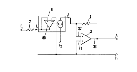
In order to explain the principle underlying the invention,
the block diagram of Figure 1 shows the circuit arrangement
of an amplifier with a set or adjustable non-inverting gain
CA 02211276 1997-10-24
7
V. The circuit arrangement has an input E and an output A,
with the result that a signal present at the input E, re-
ferring to a first reference potential P1, appears at the
output A, after having been amplified by the set gain V.
Essential parts of the amplifier are a first operational
amplifier 3, a current copier 8 having a current input and
a current output, a first resistor 1 having the resistance
R1 and a second resistor 2 having the resistance R2. The
current copier 8 is drawn by two overlapping circles which
are the commonly usual symbol of a current source.
The operational amplifier 3 has a non-inverting input 31,
which is provided with a plus symbol in the figures, as is
generally conventional in block diagrams of operational am-
plifiers, and an inverting input 32, which is provided with
a minus symbol in the figures. The output 33 of the opera-
tional amplifier 3 is simultaneously the output A of the
circuit arrangement. The non-inverting input 31 is connect-
ed to the first reference potential P1.
The output 33 is connected via the first resistor 1 to the
inverting input 32, which is connected to the current out-
put of the current copier 8. The current input of said cur-
rent copier is connected to the input E of the circuit ar-
rangement via the second resistor 2.
An input section of the current copier 8, which is a second
operational amplifier 80 in the embodiments of Figures 1
and 2, is connected to the first reference potential P1. To
be precise, in the case of the operational amplifier 80,
this is the non-inverting input thereof. Its inverting
input and its output are connected to one another and are
the current input of the current mirror 8. The output
section of the current copier 8 is connected to a second
reference potential P2.
CA 02211276 1997-10-24
8
A current flowing through the second resistor 2 and into
the input circuit of the current copier 8 and having a
current value I appears in the output circuit of said
current copier, in accordance with the essential property
of current copiers, with the same current value I and like-
wise flows into the output circuit of said current copier,
in other words the current is "copied".
Since the input resistance is ideally equal to infinity in
the case of operational amplifiers, but in reality lies in
the megohm range, the copied current having the current
value,I flows solely through the first resistor 1. Conse-
quently, the above equation (3) holds true.
In the case of the embodiment of the invention shown in
Figure 2, the second resistor 2 according to Figure 1 is
replaced by a first and a second partial resistor 21, 22
having the respective resistances R21 and R22, which par-
tial resistors are connected in series. A first switch 51
is arranged between the current input of the current copier
80 and the first partial resistor 21 and a second switch 61
is ar-ranged between this current input and a junction
point between the partial resistors 21, 22.
Consequently, it is possible to set two different values of
the gain V by correspondingly closing the respective switch
51, 61:
- When switch 61 is - as depicted - open and switch 51
is - as depicted - closed, the sum R21 + R22 of the
resistances R21, R22 is effective, and
- when switch 51 is open and switch 61 is closed, or when
both switches 51, 61 are closed, only the resistance R22
is effective.
CA 02211276 1997-10-24
9
Figure 3 shows another embodiment of the invention which is
more favorable than the embodiment according to Figure 2
when not only the current copier but also the switches 51,
61 are intended to be part of an integrated semiconductor
circuit. The switches 51, 61 are then electronic switches
in the form of transistors, and their respective internal
resistance in the on state, the so-called ON resistance, is
voltage-dependent and, in addition, is not negligible. Spe-
cifically, in the case of the circuit arrangement according
to Figure 2, the ON resistance is added to the resistances
R21~ R22~ Since the current having the value I flows via
the switches 51, 61.
The circuit arrangement of Figure 3 does not have this
disadvantage. For this purpose, in the current copier 8',
first of all the connection between the inverting input of
the second operational amplifier 80' and the output of the
latter, such a connection being present in Figure 2, is
eliminated and the inverting input itself is connected up.
To this end, a further switch 52 is arranged between the
junction point of the switch 51 with the partial resistor
21 and the inverting input of the operational amplifier
80'. In a comparable manner, a further switch 62 is con-
nected between this inverting input and the junction point
between the partial resistors 21, 22. The switches 51 and
52, and 61 and 62, thus respectively form a first and a
second series circuit of switches. In each of these series
circuits, the switches must be simultaneously closed or
open.
It is again possible to set two different values of the
gain V by correspondingly closing the respective switches
51, 52 and/or 61, 62:
CA 02211276 1997-10-24
When the switches 61, 62 are - as depicted - open and the
switches 51, 52 are - as depicted - closed, the sum
R21 + R22 of the resistances R21, R22 is effective, and
- when the switches 51, 52 are open and the switches 61, 62
5 are closed, or when all four switches are closed, only
the resistance R22 is effective.
Although, the circuit arrangement of Figure 3, too, in the
state depicted, has a voltage drop across the ON resis-
10 tance of the switch 51 generated by the current flowing
through the latter and having the value I, this voltage
drop,cannot adversely affect the voltage occurring at the
junction point of the switch 51 with the partial resistor
21, since obviously this junction point is virtually con-
nected to the first reference potential P1 via the switch
52. The same is comparably true when the switches 61, 62
are closed. This applies as long as the abovementioned
voltage drop does not limit the output voltage of the
operational amplifier 80' or drive it to saturation.
In order to ensure that the respective voltages at the cur-
rent input and at the current output of the current copier
8' are identical, provision is made of a permanently closed
switch 34, which connects the inverting input 32 of the
first operational amplifier 3 to the current output of the
current copier 8' and, naturally, is likewise realized,
like the other switches, by a semiconductor component. The
switch 34 can also been inserted into the circuits of Figs.
1 and 2, if necessary.
In the case of insulated-gate field-effect transistors as
switches, the respective width-to-length ratio of the gate
electrodes of the field-effect transistors which realize
the switches 34, 61, 62, that is to say the so-called W/L
ratio, must be made identical.
CA 02211276 1997-10-24
11
If the partial resistor 21 has a sufficiently low value,
the further switches 52, 62 can be omitted and the invert-
ing input of the operational amplifier 80' can be connected
to the junction point of the partial resistor 21 with the
switch 51.
If it is intended to be able to set more than two gain va-
lues, then the series circuit formed by the partial resis-
tors 21, 22 according to the example of Figures 2 and 3
can, of course, have further partial resistors added to it,
to which partial resistors corresponding further switches
must then be assigned.
Figure 4 shows the circuit diagram of a current copier 8
which is realized using the technology of integrated com-
plementary enhancement-mode insulated-gate field-effect
transistors, that is to say using so-called CMOS tech-
nology.
In detail, the circuit diagram of Figure 4 shows a first
series circuit 81 formed by two transistors 83, 84 which
are connected between an operating potential U and the
second reference potential P2, have their controlled cur-
rent paths connected in series and are of mutually com-
plementary conductivity types.
Furthermore, there is a second series circuit 82 formed by
two transistors 85, 86 which are connected between the
operating potential U and the second reference potential
P2, have their controlled current paths connected in series
and are of mutually complementary conductivity types; tran-
sistors 83 and 85 are p-channel transistors and transistors
84 and 86 are n-channel transistors. The control terminals
of the two transistors 83, 85 are connected to one another,
as are the control terminals of the two transistors 84, 86.
CA 02211276 1997-10-24
12
The junction point between the controlled current paths of
the transistors 83, 84 of the first series circuit 81 is
connected to the non-inverting input of a further opera-
tional amplifier 87, the inverting input of which is con-
s netted to the first reference potential P1.
The operational amplifier 87 has a differential output, one
pole of which is connected to the junction point between
the control terminals of the two transistors 84, 86 and the
other pole of which is connected to the junction point
between the control terminals of the two transistors 83,
85.
Furthermore, each of these poles is connected via a res-
pective capacitor 88 and 89 to the junction point between
the controlled current paths of the transistors of the
first series circuit 81. Depending on the specific internal
circuitry of the further operational amplifier 87, it is
also possible just to provide either the capacitor 88 or
just the capacitor 89.
Figure 4 also illustrates the behavior of the current
copier 8 with regard to the current having the value I.
This current is divided into a "positive" current Ip
flowing in the transistor 83 and a "negative" current IN
flowing in the transistor 84. Correspondingly, identical
- copied - currents I'p and I'N, respectively, flow into
the transistors 85, 86 of the second series circuit 82 and
add up to the - copied - current having the value I.
Finally, the following is also pointed out: Usually, inte-
grated semiconductor circuits which exclusively process
digital signals are fed by an operating voltage source
whose negative pole serves as circuit zero-point and can
thus also be referred to as digital circuit zero-point. In
the manufacturer's data, the potential of this digital cir-
CA 02211276 1997-10-24
13
cuit zero-point is often abbreviated to Vss and the posi-
tive potential is often designated by Vdd or Vcc. Moreover,
an operating voltage source which also has a negative volt-
age with respect to the digital circuit zero-point is not
necessary. A nowadays widespread and customary value Vdd or
Vcc of the operating voltage is +5 V.
Since analog signals can assume both positive and negata.ve
values with respect to a reference potential, which can be
l0 regarded as analog circuit zero-point, integrated semicon-
ductor circuits which process analog signals require an
operating voltage source which has both a positive and a
negative value with respect to this analog circuit zero-
point, in other words a bipolar operating voltage source.
If the reference potential is then selected to be O V,
that is literally the analog circuit "zero-point". However,
Vss must then have the value -2.5 V, for example, and Vdd
or Vcc the value +2.5 V.
For integrated semiconductor circuits which process both
analog and digital signals, referred to as mixed circuits
below, this means, for example, that the digital circuit
zero-point has a potential Vss of -2.5 V, while the analog
circuit zero-point has 0 V. However, this necessitates the
above bipolar operating voltage source. In order to avoid
this, it is frequently the case in mixed circuits that the
analog circuit zero-point is put at +2.5 V and the digital
circuit "zero-point" is put at 0 V.
Since this selection and the voltage values cited are not
mandatory, the above discussion generalized by talking of a
first and of a second reference potential P1, P2. For the
above voltage values and their polarities, the first and
the second reference potential P1, P2 respectively corres-
pond in any case to said analog circuit zero-point and the
digital circuit zero-point explained.