Note: Descriptions are shown in the official language in which they were submitted.
CA 02211678 1997-07-28
RESONATING STh~ J~5 AND
MET}~OD FO~ FORHINa TIIE R13SONATING STRUCTURE
R13LATED APPLICATIONS
This application is a continuation-in-part of co-
pending United States Patent Application Serial Nos.
08/488,146, filed June 7, 1995, and 08/480,267, filed
June 7, 1995, and claims the benefit under 35 U.S.C.
Sll9 of co-pen~ing United States Provisional Patent
Application Serial No. 60/023,819, filed August 12,
1996.
P~RGROUND OF THE ~ lON
The invention relates to transducers for measuring
force, and particularly to a silicon microelectronic
mechanical structure for measuring force. The
invention also relates to a method of forming the
microelectronic mechanical force transducer.
Semiconductor pressure transducers utilizing a
diaphragm formed of semiconductor material are commonly
known in the art. Examples of a few of such pressure
transducers are shown and described in U.S. Patent Nos.
4,744,863; 4,853,669; and 4,996,082.
It is also known in the art to use semiconductor
material to produce a resonating beam. The beam is
excited, usually using electronic means, and the
vibratory motion of the beam is detected using
electronic means. The signal generated by the
electronic means is indicative of the frequency at
which the resonating beam is vibrating and thus the
physical condition of the beam.
SUMMARY OF THE lNV~Nl-~ON
Commonly known semiconductor force transducers,
and particularly pressure transducers, typically
exhibit a low sensitivity to force. As a result,
existing semiconductor force transducers are of limited
use in measuring very low forces or very small force
changes.
CA 02211678 1997-07-28
Also, known semiconductor force transducers and
resonating beams are typically formed from a
polysilicon material which makes connection of the
electronics to the microelectronic mechanical structure
difficult and exre~sive.
Accordingly, the invention provides a force
transducer including a semiconductor substrate having a
surface defining a recess, such that the recess has a
peripheral boundary. The force transducer also
includes a flexible diaphragm connected to the surface
along the peripheral boundary to enclose the recess so
that the diaphragm ~ves in response to changes in a
force applied thereto. The force transducer also
includes a resonant beam connected to the surface
adjacent the peripheral boundary. The resonant beam
has a resonant frequency such that movement of the
diaphragm in response to changes in the force on the
diaphragm results in a change to the resonant frequency
of the resonant beam. In one embodiment of the
invention, the flexible diaphragm or the resonant beam
or both are formed from single crystal silicon.
The invention also provides a method of forming
the force transducer. The method includes the steps of
implanting in the substrate layer a one of an n-type or
p-type dopant; doping the substrate to create a first
region doped with the other of the n-type or the p-type
dopant, and a second region spaced from the first
region and being doped with the other of the n-type or
the p-type dopant; depositing an epitaxial layer on
said surface over said first and second regions;
implanting a first sinker through the epitaxial layer
and into connection with the first regent; implanting a
second sinker through the epitaxial layer and into
connection with the second region; anodizing the
~ubstrate to form porous silicon of the first and
second sinkers and of the first and second regions;
oxidizing the porous silicon to form silicon dioxide;
CA 02211678 1997-07-28
and etching the silicon dioxide to form the recess, the
flexible diaphragm, and the resonant beam.
It is an advantage of the invention to provide a
method of forming a force transducer having a single
crystal resonating beam adjacent a single crystal
diaphragm.
It is also an advantage to provide a force
tran~ducer having a ~ingle crystal resonating beam
adjacent a ~ingle crystal diaphragm.
It i~ another advantage of the invention to
provide a force transducer that can be inexpensively
formed by single-sided fabrication in relatively few
steps.
It is another advantage of the invention to
provide a force transducer of high sensitivity and
accuracy wherein the beam is integral to the substrate
of the transducer.
Other features and advantages of the invention
will become apparent to those skilled in the art upon
review of the following detailed description, claims,
and drawings.
BRIEF DESCRIPTION OF THE DRAWINGS
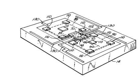
Figure 1 is an enlarged perspective view of the
microelectronic mechanical force transducer.
Figure 2 is a dark field mask for use in the step
of implanting an n-type buried layer in the structure
forming the transducer.
Figure 3 i8 a dark field mask for use in the step
of doping the structure with a p-type dopant.
Figure 4 is a top-down view of the structure after
the step of doping.
Figure 5 is a dark field mask for use in the step
of implanting sinkers through the epitaxial layer.
Figure 6 is a top-down view of the structure after
the step of implanting sinkers through the epitaxial
layer.
CA 02211678 1997-07-28
Figure 7 is a dark field mask for use in the step
of implanting the capacitor and piezoresistor.
Figure 8 is a top-down view of the structure after
the step of implanting the capacitor and piezoresistor.
Figure 9 is a clear field mask for use in the step
of creating an oxidized silicon cover over a portion of
the structure.
Figure 10 is a top-down view of the structure
after the step of creating an oxidized silicon cover.
Figure 11 is a dark field mask for use in the step
of creating anchor region-~ on the structure.
Figure 12 is a top-down view of the structure
after the step of creating anchor regions.
Figure 13 is a clear field mask for use in the
step of creating polysilicon covers at various points
on the structure.
Figure 14 is a top-down view of the structure
after the step of creating polysilicon covers at
various points.
Figure 14A is a dark field mask for use in the
step of creating an n-type sinker on the structure.
Figure 14B is a dark field mask for use in the
step of creating a p-type region in the cover layer.
Figure 14C is a top-down view of the structure
after the step of implanting the n-type sinker and the
p-type region.
Figure 15 is a dark field mask for use in the step
of creating metalization contacts on the structure.
Figure 16 is a top-down view of the structure
after the step of creating metalization contacts.
Figure 17 is a clear field mask for use in the
step of creating conductive metal current flow pathways
overlaying the metalization contacts.
Figure 18 is a top-down view of the structure
after the step of creating the conductive metal
pathways.
CA 02211678 1997-07-28
Figure 19 i8 a view taken along line 19-19 in
Figure 4 before any process steps were performed on the
~ubstrate.
Figure 20 i8 a view taken along line 20-20 in
Figure 4 after the steps of implanting the N-type layer
and doping the P-type buried regions.
Figure 21 is a view taken along line 21-21 in
Figure 6.
Figure 22 is a view taken along line 22-22 in
Figure 6.
Figure 23 is a view taken along line 23-23 in
Figure 6.
Figure 24 i8 a view taken along line 24-24 in
Figure 8.
Figure 25 is a view taken along line 25-25 in
Figure 10.
Figure 26 is a view taken along line 26-26 in
Figure 12.
Figure 27 is a view taken along line 27-27 in
Figure 14.
Figure 28 is a view taken along line 28-28 in
Figure 14.
Figure 29 is a view taken along line 29-29 in
Figure 16.
Figure 30 is an enlarged perspective view of a
force transducer that is an another embodiment of the
invention.
Figure 31 is a dark field mask for use in the step
of implanting an n-type buried layer in the structure
forming the transducer of Figure 30.
Figure 32 is a dark field mask for use in the step
of doping the structure forming the transducer of
Figure 30 with a p-type dopant.
Figure 33 is a dark field mask for use in the step
of implanting p-type sinkers through the epitaxial
layer of the structure forming the transducer of Figure
30.
-
CA 02211678 1997-07-28
Figure 34 is a dark field mask for use in the step
of implanting the capacitor and piezoresistor in the
structure forming the transducer of Figure 30.
Figure 35 is a clear field mask for use in the
step of creating an oxidized silicon cover over a
portion of the structure forming the transducer of
Figure 30.
Figure 36 i~ a dark field mask for use in the ~tep
of creating A~chor regions on the structure forming the
trAnq~ er of Figure 30.
Figure 37 is a clear field mask for use in the
step of creating polysilicon covers at various points
on the structure forming the transducer of Figure 30.
Figure 38 i8 a dark field mask for use in the step
of creating an n-type sinker on the structure forming
the transducer of Figure 30.
Figure 39 is a dar~ field mask for use in the step
of creating a p-type region in the cover layer of the
transducer of Figure 30.
Figure 40 is a dark field mask for use in the step
of creating metalization contacts on the structure
forming the transducer of Figure 30.
Figure 41 is a clear field mask for use in the
step of creating conductive metal current flow pathways
overlaying the metalization contacts.
Before one embodiment of the invention is
explained in detail, it is to be understood that the
invention is not limited in its application to the
detail~ of construction and the arrangement of
components ~et forth in the following description or
illustrated in the drawings. The invention i9 capable
of other embodiments and of being practiced or being
carried out in various ways. Also, it is to be
understood that the phraseology and terminology used
herein is for the purpose of description and should not
be regarded as limiting.
CA 02211678 1997-07-2X
D~TAIT~n DESCRIPTION OF THE P~FERRED ~RODIM~NT
Illustrated in Fig. 1 of the drawings i~ a force
transducer 10 embodying the invention. Although
various types of force transducers such as pressure
sensors, strain sensors and displacement sensors may be
formed according to the invention, the force transducer
10 is a pressure sensor.
As shown specifically in Figs. 19-29, the force
transducer 10 is formed from a sub~trate 14 of single
crystal silicon which is altered a~ set forth below in
the description of the method of making the transducer
10. In the preferred embodiment, the substrate 14 is a
p-type silicon wafer of lightly doped P(100) silicon
having p-type boron dopant with a carrier concentration
between 10l5 and 10l6 cm~3~ a <100> cut lattice, 6.0-18.0
ohm-cm resistance. Wafers meeting SEMI st~n~Ard prime
CZ or float zone, for example, are suitable. Examples
of other suitable silicon wafers are those having lower
concentrations of p-type or n-type dopants than layers
to be subsequently added to the wafer, such that the
dopant acts as an etch stop at the boundary with the
added layers. Referring generally to Figs. 19-29, the
substrate 14 includes a horizontal upper surface 18.
Although the substrate 14 can be of any suitable
thickness, in the illustrated embodiment, the substrate
14 is about 500 microns thick.
The upper surface 18 defines an elongated cavity
or recess 22 (Figs. 28 and 29) having a pair of spaced
sidewall surfaces 26 (only one of which is shown in
Fig. 29), a pair of spaced end wall surfaces 34
extending between the sidewall surfaces 26, and a
horizontal bottom surface 42 extending between the
sidewall surfaces and end wall surfaces. The sidewall
surfaces 26, end wall surfaces 34 and bottom surface 42
thus cooperate to define the cavity 22. The upper
surface 18 also defines two square cavities or recesses
46 and 50 adjacent respective end wall surfaces 34.
More particularly, the cavities 46 and 50 include
CA 02211678 1997-07-28
peripheral boundaries 54 and 58 adjacent the end wall
surfaces 34, respectively.
An epitaxial layer 60 is deposited on the upper
surface 18. The epitaxial layer 60 includes a center
portion forming a plate or beam 62 (best shown in Figs.
22 and 23) which extends across the cavity 22. In the
embodiment illustrated in Fig. 1, the beam 62 has a
longitl~i n~l axis 66 and includes opposite end portions
70 engaging the upper surface 18 adjacent the end wall
surf~ces 34 so that the beam 62 is capable of
~e~on~ting at a given frequency in response to a
stimulus. In other embodiments, the resonant plate or
beam 62 may be circular or another shape and include an
edge portions. Hereinafter, the term end portions is
defined to include any edge portion of the plate or
beam 62, notwithstAn~ing the actual shape of the plate
or beam 62. Engagement of the beam 62 to the upper
surface 18 at the end portions 70 allows strain in the
epitaxial layer 60 (or in the substrate 14) in the
direction of the longitudinal axis 66 of the beam 62 to
change the resonant frequency of the beam 62. In the
specific embodiment illustrated, the beam 62 is part of
the epitaxial layer 60. In other embodiments (not
shown), the beam 62 can be formed partially in the
epitaxial layer 60 and in the upper surface 18 of the
substrate 14. Also the beam 62 can be of any suitable
length, however, in the illustrated embodiment, the
length of the beam 62 is about 100 ym. The beam 62
includes an upper surface 72 and a lower surface 74
spaced from the bottom wall 36. The beam 62 has a
thickness of about 1.5 microns between the upper and
lower surfaces 72 and 74, respectively. The beam 62
also includes a pair of oppositely facing side surfaces
82 (only one of which is shown in Figs. 1 and 28)
extending between the upper and lower surfaces 72 and
74. The side surfaces 82 are generally parallel to the
side wall surfaces 26. The beam 62 also has a width
defined by the distance between the side surfaces 82,
CA 02211678 1997-07-28
which, in the illustrated embodiment, is about 20
microns.
The epitaxial layer 60 includes two diaphragm
portions 86 and 90 adjacent the respective end portions
S 70 of beam 62. The diaphragm portions 86 and 90 cover
the sguare cavities 46 and 50, respectively. The
~i~phragm portions 86 and 90 each include five sealed
apertures 94 (shown in the ~unsealed~ state in Fig. 6)
formed therein. As described in greater detail below,
the sealed apertures 94 facilitate fabrication of the
transducer 10 and are formed and sealed during
fabrication of the transducer 10. The diaphragm
portions 86 and 90 are deflectable, either upwardly or
downwardly, in response to a change in the force or
pressure applied to the diaphragm portions 86 and 90.
Novement of the diaphragm portions 86 and 90 changes
the strain in the beam 62 and thereby changes the
frequency at which the beam 62 resonates.
The transducer 10 also includes a cover layer 98
mounted on the epitaxial layer 60. The cover layer 98
includes a center portion 102 spaced from the upper
surface 72 of the beam 62, and a periphery 106
supporting the cover layer 98 on the epitaxial layer 60
so as to completely cover the beam 62 and seal the
cavity 22. In other words, the cover layer 98
cooperates with the side walls 26, end walls 34 and
bottom wall 42 of the upper surface 18 to enclose the
cavity 22 and thus define a closed space about the beam
62 so that the beam 62 can resonate within the cavity
22. Although any suitable material is appropriate, in
the illustrated emb~diment, the cover layer 98 consists
of polysilicon having a thickness of about 2 microns.
Although the space between the cover layer 98 and the
upper surface 72 of the beam 62 can be of any suitable
dimension, in the illustrated embodiment the cover
layer 98 is spaced about 1 micron above the upper
surface 72 of the beam 62. As described in greater
CA 02211678 1997-07-28
--10--
detail below, the cavity 22 is preferably evacuated to
minimize mechanical damping of the resonating beam 62.
The transducer 10 also includes covers 110
(numbered in Figs. 1, 14 and 27-29 only), which cover
the apertures 94 in the diaphragm portions 86 and 90 to
completely seal the cavities 46 and 50. Although any
suitable material is appropriate, in the illustrated
embodim~nt, the covers 110 consist of polysilicon
having a thickness of about 2 microns.
The transducer 10 includes means for causing
resonant motion of the beam 62. Although any suitable
mechanical or electrical means can be employed for
causing resonant ~ tion of the beam 62, in the
illustrated embodiment, the means for causing resonant
motion of the beam 62 includes a pair of electrodes 114
and 118 (best shown in Fig. 29) which cooperate in
response to an electrical stimulus to define a
capacitive drive. The electrodes 114 and 118 are
electrically connected to circuitry (not shown) to
control the capacitive drive. It will be apparent to
those skilled in the art that the beam 62 is caused to
vibrate or resonate by operation of the capacitive
drive in a known manner. It is also apparent that
various combinations of dopants can be used to form the
electrodes 114 and 118.
The transducer 10 includes means for measuring
resonating motion of the beam 62. Although any
suitable means can be used for measuring resonating
motion of the beam 62, in the illustrated embodiment
the means for measuring resonating motion of the beam
62 is a piezoresistor 122. The piezoresistor 122 is
created by implanting in the beam 62, a dopant, such as
boron. The piezoresistor 122 is connected to
integrated circuitry (not shown) in manner well known
to those of ordinary skill in the art. The resistance
of the piezoresistor 122 changes with strain in the
beam 62 in accordance with the piezoresistive effect,
and thus permits resonance of the beam 62 to be
CA 02211678 1997-07-28
measured in a known manner. It will be appreciated by
those skilled in the art that in different embodiments
(not shown)~ other arrangements of passive electronic
circuit elements (e.g., a capacitor, etc.) or of active
electronic circuit elements (e.g., operational
amplifiers, etc.) can be used for measuring the
frequency of resonance of the beam 62. Moreover, the
single crystal nature of the beam 62 allows the
placement of active or passive signal conditioning
circuitry (not shown) to be implanted directly on the
beam 62.
The transducer 10 includes metal contacts 126 and
electrical conductors 130 connected to the metal
contacts 126 for providing a means of connecting the
electrodes 114 and 118 and piezoresistor 122 to other
circuitry (not shown). In the illustrated ~mho~iment~
the metal contacts 126 are aluminum, which is deposited
on the epitaxial layer 60. In other embodiments (not
shown), the electrical contacts may be formed by
dopants implanted to define conductive regions.
The transducer 10 having the specific construction
described herein is formed by altering the p-type
substrate 14 according to the following steps:
1. implanting buried n-type layer 134 in the p-
type substrate 14 using the mask shown in Fig. 2 (see
Fig. 20);
2. implanting buried p-type layer 138 using the
mask shown in Fig. 3 (see Fig. 20);
3. depositing an epitaxial n-type layer 60 on the
upper surface 18 of the substrate 14 (see Fig. 21);
4. implanting p-type sinkers 142 through the
epitaxial n-type layer 60 and into connection with the
p-type layer 138 using the mask shown in Fig. 5 (see
Figs. 21 and 22);
5. forming porous silicon of the p-type layer 138
and the p-type sinkers 142 by anodization;
6. oxidizing the porous silicon to form silicon
dioxide in three pre-cavity regions;
CA 02211678 1997-07-28
7. implanting p-type layers (i.e., electrode 114
and piezoresistor 122) in the epitaxial n-type layer 60
using the mask shown in Fig. 7;
8. depositing a layer of sacrificial material;
9. etching the layer of sacrificial material
using mask shown in Fig. 9 to form the sacrificial
layer 150 See Fig. 25);
10. growing anchor oxide 152;
11. forming anchor cavities 154 (see Fig. 27) by
etching anchor oxide using the mask shown in Fig. 11;
12. depositing the cover layer 98 using the mask
shown in Fig. 13;
13. etching the cover layer 98;
14. dissolving the sacrificial layer 150 and the
porous silicon dioxide by etching to form the cavities
22, 46 and 50;
15. sealing and evacuating the cavities 22, 46
and 50 (see Figs. 28 and 29);
16. depositing an insulating layer;
17. implanting an n-type sinker 158 on the
epitaxial layer 60 using the mask shown in Fig. 14A;
18. implanting a p-type region (i.e., electrode
118) on the cover layer 98 using the mask shown in Fig.
14B;
19. etching metal contacts 126 through the
insulating layer using the mask shown in Fig. 15; and
20. depositing electrical conductors 130 using
the mask shown in Fig. 17 to connect the transducer 10
to integrated circuitry (not shown).
It will be appreciated by those skilled in the art
that various of the above-mentioned steps may be
omitted or altered in different specific embodiments of
the invention. For example, the steps regarding the n-
type layer, and the p-type layers may differ if
different means are employed for causing resonance of
the beam 62 or for measuring the resonant frequency of
the beam 62.
CA 02211678 1997-07-28
In the illustrated embodiment, the substrate 14 iq
prepared for implantation of the buried n-type layer
134 by initially forming a screening layer of SiO2 on
the upper surface 18 of the substrate 14. In the
illustrated embodiment, the screening layer of SiO2 has
a thickness of about 5000 +/- 500 angstroms. Oxidation
to form the SiO2screening layer i8 carried out by
first "pushing~ with about 2.25 liters per minute (l/m)
of N2 at a temperature of about 550~C for a period of
about 4 hours, ramping about 2.25 l/m Of ~2 gas at a
rate of about 20~C/minute, oxidizing with about 2.25
l/m of H2 and ~2 at about 1000~C, and then ramping with
about 8 l/m of N2 at a rate of about 20~C/minute. The
term "pushing~ as used herein means inserting the wafer
into the furnace. As also used herein, the term
n ramping" means changing the temperature in the
furnace.
The SiO2 screening layer is thereafter etched to
achieve a substantially uniform thickness. Etching
with a 10:1 buffered oxide etching solution for a
period of about 5 minutes is suitable. A suitable
etching solution includes about 40% ammonia fluoride,
15% hydrogen fluoride and 45% water. Those skilled in
the art will recognize that forming and etching a
screening layer of SiO2 before each implant or
deposition step may assist in control of the subsequent
implantation or deposition step. In other embodiments,
any of the screening layers of SiO2 may be omitted.
The buried n-type layer 134 is implanted by
applying photoresist to the substrate 14 and then
exposing the photoresist with the buried n-type layer
mask shown in Fig. 2, removing the mask, and then
dosing with a suitable n-type dopant. In the
illustrated embodiment, the n-type dopant is
phosphorous, which is dosed at a concentration of 5 x
10l3 cm~2 at 150 ReV. After the photoresist is removed,
the buried n-type layer 134 is driven to a final
thickness of about 2 to 4 microns by thermal annealing.
CA 022ll678 l997-07-28
-14-
Thermal annealing can be carried out in any suitable
manner, such as by pushing with 2.25 l/m of N2 at 850~C
for a period of about 30 minutes, ramping 2.25 l/m of
~2 at a rate of 20~C/minute, oxidizing with 2.25 l/m of
N2 at about 1100~C for a period of about 17 hours, and
ramping with 8 l/m of N2 at a rate of 20~C/minute. The
thermal annealing conditions specifically described
above are provided for illustration, and tho~e skilled
in the art will appreciate that different conditions
may be used to achieve this reQult.
The buried p-type layer 138 is implanted over the
buried n-type layer 134 by first etching the substrate
14 for 5 minutes to remove the SiO2formed in the
previous thermal annealing step. The buried p-type
layer 138 is patterned by applying photoresist to the
substrate 14 and exposing the photoresist with the mask
shown in Fig.-3. In the illustrated embodiment, the p-
type dopant is boron. The boron is dosed at a
concentration of 5 x 10l3 cm~2 at consecutive energy
levels of 50, 100 and 150 ReV. After the buried p-type
layer 138 is implanted and the photoresist is removed,
the buried p-type layer 138 is driven by thermal
annealing to a final thickness of about 1 ~m. Thermal
~nne~ling can be carried out by pushing with 2.25 l/m
Of ~2 at 850~C for a period of about 30 minutes,
ramping 2.25 l/m of ~2 at a rate of 20~C/minute,
annealing with 2.25 l/m of N2 at about 1000~C for a
period of about 1 hour and 40 minutes, and ramping with
8 l/m of N2 at a rate of 20~C/minute.
The n-type epitaxial layer 60 is deposited on the
entire upper surface 18 of the substrate 14 by
epitaxial deposition. In the illustrated embodiment,
the substrate 14 the n-type epitaxial layer 60 is
deposited by etching the substrate 14 to remove the
SiO2 formed in the previous thermal annealing step.
The n-type epitaxial layer 60 is deposited in a
conventional manner. In the illustrated embodiment,
the n-type epitaxial layer 60 has a thickness of about
CA 02211678 1997-07-28
2 +/- 0.2 microns and a resistivity of about 0.04 +/-
0.02 ohms-cm.
The p-type sinkers 142 are implanted in the n-type
epitaxial layer 60 and into electrical connection with
S the p-type layer 138. In the illustrated embodim4nt,
the n-type epit~Yi~l layer 60 i8 partially oxidized to
form a screening layer of SiO2 having a thickness of
about 500 +/- 50 angstroms. The SiO2 can be formed by
first ~pushing~ with about 2.25 liters per minute (l/m)
of EI2 and ~2 at a temperature of about 850~C for a
period of about 10 minutes, and then oxidizing with
about 2.25 l/m of EI2 and ~2 at about 850~C for a period
of about 30 minutes. The p-type sinkers 142 are
patterned by applying photoresist and exposing the
lS photoresist with the mask shown in Fig. 5. In the
illustrated embodiment, the p-type dopant is boron
dosed at a concentration of 4 x 10l4 cm~2 at an energy
level of 175 ReV. After the p-type sinkers 142 are
implanted, the photoresist is removed.
The p-type layer 138 and the p-type sinkers 142
are anodized to form a pre-cavity region consisting of
porous silicon. Those skilled in the art will
appreciate that anodization of the p-type layer 138 and
the p-type sinkers 142 is an electrochemical process
which can be carried out in any suitable manner. In
the illustrated embodiment, anodization is carried out
in an electrochemical cell containing from 10 to 50
weight percent hydrofluoric acid. The electrochemical
cell is separated into two chambers by the substrate 14
being anodized. Two platinum plates serve as the
anodic and cathodic electrodes. The back or lower side
portion of the substrate 14 faces the anodic electrode
and the upper side portion 16 faces the cathodic
electrode. An anodization voltage between about 1 and
7 volts is applied across the electrodes. The
anodization process automatically stops when the low
resistance p-type layer 138 and p-type sinkers 142 are
converted into porous silicon. The porous silicon thus
CA 02211678 1997-07-28
defines a pre-cavity region in the area previously
occupied by the p-type layer 138 and p-type sinkers
142.
The porous silicon in the pre-cavity region is
oxidized to form silicon dioxide. The porous silicon
is oxidized by first ~pu hing" with about 2.25 liters
per minute (l/m) Of ~2 at a temperature of about 300~C
for a period of about 1 hour to stabilize the porous
silicon, ramping with 2.25 l/m Of ~2 at 20~C/minute,
and oxidizing with 2.25 l/m of Hl and ~2 at 850~C for
about 30 minutes to 1 hour, uch that the oxide
thickness i~ between about 1000-3000 angstrom~. In the
illustrated embodiment, the maximum oxidation
temperature is maintained at 850~C in order to avoid
inelastic change in the resulting oxide. Upon
oxidation, the porous silicon in the pre-cavity region
- i converted to silicon dioxide, and a layer of silicon
dioxide having a thickness of about 1500 angstroms is
incidentally formed over the entire upper surface of
the n-type epitaxial layer 60.
The p-type layer (i.e., electrode 114 and
piezoresistor 122) is implanted in the n-type epitaxial
layer 60 is patterned by applying photoresist and
exposing the photoresist with the mask shown in Fig. 7.
In the illustrated embodiment, the p-type dopant is
boron dosed at a concentration of 5 x 10'5 cm~2 at an
energy level of 80 KeV. After the p-type layer is
implanted and the photoresist is removed, the p-type
layer is annealed. In the illustrated embodiment, the
p-type layer is annealed by pushing ~ith 2.25 l/m of N2
at 850~C for a period of 10 minutes and oxidizing with
2.25 l/m of N2 at 850~C for 30 minutes.
A layer of sacrificial material is deposited over
the entire n-type epitaxial layer 60 and pre-cavity
regions and then etched to define the sacrificial layer
150. In the illustrated embodiment, the sacrificial
material is deposited over the n-type epitaxial layer
60. The sacrificial material is a low temperature
CA 02211678 1997-07-28
oxide glass (LTO glass) having a thickness of about 1
micron. The LTO glass is deposited in a known manner,
~uch as by chemical vapor deposition (CVD). In other
embodiments, the sacrificial layer 150 can be silicon
nitride or another suitable material. The LTO glass is
patterned by applying photoresist and exposing the
photoresist with the mask shown in Fig. 9. The LTO
glass is etched and the mask is removed to leave the
sacrificial layer 150. Etching with a 10:1 buffered
oxide etching solution for a period of about 10 minutes
is suitable to form the sacrificial layer 150. The
photoresist thereafter i8 removed.
The substrate 14 is prepared for receiving the
cover layer 98 by forming anchor cavities 154 in a
layer of anchor oxide. In the illustrated embodiment,
the anchor cavities 154 are formed in a layer of SiO2.
A suitable layer of SiO2 having a thickness of about
1500 angstroms can be formed by oxidizing with 2.25 l/m
of E~2 and ~2 at 850~C for a period of 30 minutes. The
anchor cavities 154 are patterned by applying
photoresist and exposing the photoresist using the
anchor mask shown in Fig. 11. The wafer is etched to
form the anchor cavities 154 in the layer of SiO2.
Etching with a 10:1 buffered oxide etching solution for
a period of about 1.5 minutes is suitable to form the
anchor cavities 154. The photoresist thereafter is
removed.
A layer of cover material is deposited over the
entire upper side portion of the wafer and then etched
to define the cover layer 98. Any suitable cover
material can be used. In the illustrated embodiment,
the cover material is polysilicon deposited on the
wafer by low pressure chemical vapor deposition
(LPCVD). The polysilicon is suitably deposited at a
temperature of about 580~C to about 650~C to a
thickness of about 1 to 2 microns. The polysilicon
thus deposited is firmly secured to the wafer by
polysilicon which fills the anchor cavities 154 and
CA 02211678 1997-07-28
thus defines integral polysilicon anchors. The cover
layer 98 i~ patterned by applying photore~i~t and
exposing the photoresist using the cover mask shown in
Fig. 13. The polysilicon is etched to form the cover
layer 98. Any suitable polysilicon etching technique
can be used. For example, plasma etching with SF6 is
suitable to form the cover layer 98. The photoresi~t
thereafter is removed.
The porous silicon dioxide in the pre-cavity
region~ is removed or dissolved by etching to form the
cavities 22, 46 and 50. Any suitable etchant may be
employed. In the illustrated embodiment, the etchant
is hydrofluoric acid vapor. The use of hydrofluoric
acid vapor to etch the cavities 22, 46 and 50
eliminates the need to later dry the cavities 22, 46
and 50. In other embodiments, such as when a liquid
etchant is used, it may be necesQary to rinse the
cavities 22, 46 and 50 with water and to dry the
cavities 22, 46 and 50 by a technique such as
sublimation of cyclohexane, as is ~nown in the art.
The hydrofluoric acid vapor etches away the SiO2
between the anchors, thus forming open etch channels in
the layer underneath the cover layer 98, and thereafter
etches away the LTO glass forming the sacrificial layer
150 and the silicon dioxide in the pre-cavity regions.
The cavities 22, 46 and 50 thus formed are open, in the
sense that the etch channels were formed by etching in
the spaces between the anchors and underneath the cover
layer 98.
The cavities 22, 46 and 50 are sealed and
evacuated using any suitable method. Such methods are
commonly known in the art and are specifically shown
and described in U.S. Patent Nos. 4,744,863; 4,853,669;
4,897,360; 4,996,082; 5,090,254; and 5,104,693; which
are incorporated herein by reference. It is preferred
to evacuate the cavity 22 in order to maximize Q of the
resonating beam 62 and to evacuate the cavities 22, 46
and 50 so that they are capable of deflecting in
CA 02211678 1997-07-28
--19--
response to changes in ambient pressure. In the
illustrated embodiment, the wafer is oxidized to form
residual SiO2 layers on the inner surfaces defining the
cavities 22, 46 and 50 and the etch channels. The
residual SiO2 layers can be formed by oxidation by
pushing 2.25 l/m of H2 and ~2 at 850~C for 10 minutes
and oxidizing with 2.25 l/m of El2 and ~2 at 850~C for
30 minutes. The SiO2 layers formed on the inner
surfaces of the etch channels substantially closes the
etch channels.
The etch ch~nnels are further sealed by depositing
sealing polysilicon which fills any openings which may
remain between the SiO2 layers. In the illustrated
embodiment, the sealing polysilicon is deposited at
580~C to 650~C to a final thickness of about 1200 +/-
120 angstrom~. Excess amounts of the deposited sealing
polysilicon thereafter are etched away, leaving--
residual sealing polysilicon which fills and closes any
openings in the SiO2 layer. The sealing polysilicon
can be etched in any suitable manner. In the
illustrated embodiment, the sealing polysilicon is
isotropically plasma etched with SF6. The photoresist
thereafter is removed. Upon sealing the etch channels,
~2 remaining in the cavities 22, 46 and 50 continues to
react until substantially all ~2 in the cavities 22, 46
and 50 is consumed. The cavities 22, 46 and 50 are
thus sealed and evacuated.
The insulating layer is deposited over the cover
layer 98 and the n-type epitaxial layer 60 in a
suitable manner. Any suitable insulating material can
be used. In the illustrated embodiment, the insulating
material is silicon nitride. In the illustrated
embodiment, the silicon nitride is deposited by low
pressure chemical vapor deposition (LPCVD) at 835~C to
a thickness of about 950 +/- 90 angstroms. The
insulating layer insulates the force transducer 10 from
undesired electrical contact.
CA 02211678 1997-07-28
-20-
The n-type sinker 158 is implanted through the n-
type epitaxial layer 60 and into electrical connection
with the n-type layer. The n-type sinker 158 i8
patterned by applying photoresist and exposing the
photoresist with the mask shown in Fig. 14A. In the
illustrated embodiment, the n-type dopant is
phosphorous dosed at a concentration of 5 x 10l5 cm~2 at
an energy level of 80 ReV. After the n-type sin~er 158
is implanted and the photoresist is removed, the p-type
sinkers and the n-type sinker 158 are driven to final
thickness by thermal ~nn~Aling. Thermal annealing can
be carried out in any suitable manner, such as by
pushing with 2.25 l/m of N2 at 850~C, ramping with 2.25
l/m Of ~2 at a rate of 20~C/minute, annealing with 2.25
l/m of N2 at about 1050~C for a period of about 8.5
hours, and ramping with 8 l/m of N2 at a rate of
20~C/minute to 850~C.
The p-type region (i.e., electrode 118) is
implanted in the polysilicon cover layer 98 by applying
photoresist and exposing the photoresist with the mask
shown in Fig. 14B. While many different combinations
and concentrations of dopant are possible, the p-type
dopant of the illustrated embodiment is boron dosed at
a concentration of between 5 x 10l~ cm~2 and 5 x 10l5 cm~2
at an energy level of 60-160 Kev. After the p-type
region is implanted, the photoresist is removed.
The metal contacts 126 are deposited in a suitable
manner for connection to integrated circuitry (not
shown). In the illustrated embodi~Pnt, electrical
contact cavities are etched for receiving the
electrical contacts. The electrical contact cavities
are patterned by applying photoresist and exposing the
photoresist using the electrical contact cavity mask
shown in Fig. 15. The insulating layer is etched with
a 50:1 buffered oxide etching solution for a period of
about 2.5 minutes to form the electrical contact
cavities 235. The photoresist thereafter is removed.
The electrical contacts are then deposited in the
-
CA 02211678 1997-07-28
electrical contact cavities. In the illustrated
embodiment, the electrical contacts are aluminum. The
alllm;num i8 depo~ited to a thickness of about 7500
angstroms and etched using the mask shown in Fig. 17.
Thereafter, the aluminum electrical contacts are
alloyed into contact with the silicon by alloying at
450~C with 15~ H2 and 85% N2.
In operation of the force transducer 10, the beam
62 is cau~ed to resonate by operation of the capacitive
drive. r~al~se the re~i~tance of the piezore8i~tor 122
changes with each movement of the beam 62, the
oscillation of the beam 62 causes oscillation of the
value of the resistance of the piezoresistor 122.
Force exerted on the diaphragms causes stress or strain
in the beam 62 in the direction of the longitudinal
axis 66 of the beam 62. This stress/strain changes the
frequency at which the beam 62 is resonating. The
change in frequency can be detected electronically,
using signal conditioning circuitry (not shown), by
detecting the changing resistance of the piezoresistor.
This change in frequency is indicative of the change in
the force applied to the diaphragms.
Fig. 30 illustrates a force transducer 200 that is
another embodiment of the invention. Like parts are
identified using like reference numerals. As shown in
Fig. 30, the transducer 200 includes a substrate 14
having an upper surface 18. The upper surface 18
defines a generally circular cavity or recess 204
having a peripheral boundary 208, and an annular
cavity, recess or channel 212 surrounding the recess
204. The annular recess 212 has inner and outer
peripheral boundaries 216 and 220, respectively, with
the peripheral boundary 208 adjacent the peripheral
boundary 216.
The transducer 200 includes an epitaxial layer 60
formed on the upper surface 18 so as to define a
resonant plate or beam 224 over the recess 204 and a
flexible diaphragm 226 over the recess 212. The plate
CA 02211678 1997-07-28
224 includes a center portion 228, a lower surface 232
facing the upper surface 18 of the substrate over the
region of the recess 204, and an upper surface 236.
The plate 224 also includes a passageway 240 extending
between the upper surface 236 and the lower surface
232.
The diaphragm 226 includes an upper surface 244
and a lower surface 248 and eight passageways 2S2 (only
two of which are shown in Fig. 30) e~ten~ing between
the upper surface 244 and the lower surface 248. Eight
covers 256 (only six of which are shown in Fig. 30) are
mounted on the diaphragm 226 to enclose the passageways
252, respectively. Similar to the operation of the
transducer 10, movement of the diaphragm 226 in
response to a change in the force on the diaphragm 226
changes the stress or strain in the resonant plate 224,
which stress or strain in turn changes the frequency at
which the plate 224 resonates.
The transducer 200 also includes a cover layer 260
mounted on the epitaxial layer 60. The cover layer 260
completely encloses and seals the plate 224 within an
evacuated cavity 264, which cavity 264 includes the
recess 204.
The transducer 200 also includes means for causing
resonant motion of the beam 224. Although any suitable
mechanical or electrical means can be employed for
causing resonant motion of the beam 224, in the
illustrated embodiment, the means for causing resonant
motion of the beam includes a pair of electrodes 168
and 172 Electrode 168 is formed using the mask shown
in Fig. 31, electrode 170 is formed using the mask
shown in Fig. 34, and electrode 172 is formed using the
mask shown in Fig. 39. Electrodes 168, 170 and 172
cooperate in response to an electrical stimulus to
define a capacitive drive. The electrodes 168, 170 and
172 are electrically connected to circuitry (not shown)
to control the capacitive drive. It will be apparent
to those skilled in the art that the beam 224 is caused
CA 02211678 1997-07-28
-23-
to vibrate or resonate by operation of the eapaeitive
drive in a known manner. In other embodiments, sueh as
that shown in Fig. 1, it is possible to eause resonanee
of the beam using only two capacitor plates. It is
S also apparent that various eombinations of dopants can
be u~ed to form the eleetrodes 168, 170 and 172.
The transdueer 200 ineludes means for mea~uring
resonating motion of the beam 224. Although any
suitable means ean be used for measuring resonating
motion of the beam 224, in the illustrated embcdiment
the means for measuring resonating ~tion of the beam
224 is a piezoresistor 176. The piezoresistor 176 is
ereated by u~ing the mask shown in Fig. 34 to implant
in the beam 224, a dopant, sueh as boron. The
piezoresistor 176 i8 eonnected to integrated eireuitry
(not shown) in manner well known to those of ordinary
skill in the art. The resistanee of the piezoresistor
176 ehanges with strain in the beam 224 in aeeordanee
with the piezoresistive effect, and thus permits
resonanee of the beam 224 to be measured in a known
manner. It will be appreeiated by those skilled in the
art that in different embodiments (not shown) other
arrangements of passive eleetronie eireuit elements
(e.g., a eapaeitor, ete.) or of aetive eleetronie
eircuitry (e.g., operational amplifiers, etc.) ean be
used for measuring the frequency of resonanee of the
beam 224. Moreover, the single crystal nature of the
beam allows the placement of other active or passive
signal eonditioning cireuitry (not shown) to be
implanted direetly on the beam 224.
The transducer 200 is formed using the same
process steps used to form the transducer 10. However,
instead of using the masks shown in Figs. 2, 3, 5, 7,
9, 11, 13, 14A, 14B, 15, and 17, the transdueer 200 is
formed using the masks shown in Figs. 31-41,
respectively. Figs. 31-41 include reference or
alignment bloeks 180 for use in aligning the masks
shown in Figs. 31-41 with respect to one another.
CA 02211678 1997-07-28
Various features and advantageQ of the invention
are set forth in the following claims.