Note: Descriptions are shown in the official language in which they were submitted.
CA 02211760 1997-07-30
Doc.No.FP389 Patent
OPTICAL INTEGRATED CIRCUIT FOR BIDIRECTIONAL COMMWNICATIONS
AND METHOD FOR PRODUCING THE SAME
FIELD OF THE lWVl~ lON
The present invention relates to an optical integrated
circuit for bidirectional communication and a method for
producing the same mainly utilized with an optical fiber
communication system.
R~CKGROUN-D OF THE lNVl!iL.~ lON
Fig.6 shows one an exemplary configuration of an
optical fiber communication system for a subscriber system.
The system proposes a low-speed communication service of
POTS (Plain Old Telephone Service) (for example, telephone
service, etc.) and a high-speed communication service which
is mainly a transmission of video signals, etc.
In the same drawing, optical transmitter-receiver
equipment 5 installed in a station l is connected to the
respective optical transmitter-receiver facilities 5 of a
plurality (N units) of subscriber houses 2 via an optical
fiber transmission cable 3 and a l:N star coupler 4, and the
optical transmitter-receiver facilities 5 in the station l
and the respective subscriber houses 2 respectively have an
optical wavelength division multiplexer (WDM) l0, lx2
optical coupler 9, laser diode 6, and photo diode 8.
Furthermore, Fig.7 shows optical transmitter-receiver
equipment 5 in a subscriber house 2, wherein a light
emission drive circuit 12 and a modulation circuit 57 are
connected to the laser diode 6, and a reverse bias
I
CA 02211760 1997-07-30
, Doc.No.FP389 Patent
impression device 13, an optical receiver drive circuit 51
and a receiver demodulation circuit 14 are connected to the
photo diode 8. Furthermore, a picture signal receiver such
as video 11, etc. is connected to the optical wavelength
division multiplexer 10.
In the optical transmitter-receiver equipment 5 in a
subscriber house 2, when both communication signal light of
wavelength ~1 (for example 1.31~m) and picture signal light
as non-communication light of wavelength ~2 (for example
1.55~m) different from the above communication signal light
enter the optical wavelength division multiplexer 10, the
same permits the communication signal light of wavelength ~1
to be transmitted to the lx2 optical coupler 9 side and, on
the other hand, the same permits the picture signal light of
wavelength ~2 to be transmitted to the video 11 side.
The lx2 optical coupler 9 transmits communication
signal light inputted through the optical wavelength
division multiplexer 10 to the photo diode 8 side.
Furthermore, the lx2 optical coupler 9 is constructed so
that transmission light (communication signal light) of
wavelength ~1, which is transmitted from the laser diode 6,
enters the same, wherein the lx2 optical coupler 9 transmits
this communication signal light to the optical wavelength
division multiplexer 10 side. Transmission of communication
signal light by the laser diode is carried out by the light
emission drive circuit 12 and modulation circuit 57.
The photo diode 8 functions as a semiconductor light
reception element, and if the reverse bias impression device
CA 02211760 1997-07-30
. Doc.NoFP389 Patent
13 for impressing reverse bias voltage is driven by the
light reception drive circuit 51, the reverse bias voltage
is impressed to the photo diode 8. At this time, an optical
current responsive to the modulation of the communication
signal light incident into the photo diode 8 is detected by
the reception demodulation circuit 14.
When an optical communication is carried out between
the station 1 side and a subscriber house 2 side by a system
shown in Fig.6 using such an optical transmitter-receiver
equipment 5, for example, the communication signal light is
made incident into an optical fiber transmission cable 3 via
the lx2 optical coupler 9 and optical wavelength division
multiplexer 10 by driving the laser diode 6 secured at the
station 1 side optical transmitter-receiver equipment 5 and
transmitted via the optical fiber transmission cable 3.
Thereafter, the communication signal light is inputted into
the optical transmitter-receiver equipment 5 at the
subscriber house 2 side. Thereby, this inputted
communication signal light is transmitted to the optical
wavelength division multiplexer 10, lx2 optical coupler 9
and photo diode 8 in the optical transmitter-receiver
equipment 5 of a subscriber house 2 in order, and the same
communication signal light is received by the photo diode 8
and is detected by the reception demodulation circuit 14 as
an optical current as described above.
Furthermore, to the contrary, when communication signal
light is transmitted from a subscriber house 2 to the
station 1 side, the laser diode 6 in the transmitter-
receiver equipment 5 of the subscriber house 2 is driven to
transmit the communication signal light through the lx2
CA 02211760 1997-07-30
Doc.No.FP389 Patent
optical coupler 9 and optical wavelength division
multiplexer 10 in order and to transmit the same through an
optical fiber transmission cable 3. The communication signal
light transmitted through the optical fiber transmission
cable 3 is received by the optical transmitter-receiver
equipment 5 in the station 1 side in compliance with the
same actions as those at the optical transmitter-receiver
equipment 5 of the abovementioned subscriber house 2 side.
I0 Furthermore, for example, as shown in Fig.6, when
picture signal light of wavelength ~2 is transmitted from a
picture signal light transmission device 67 at the station 1
side, this picture signal light is transmitted to the
optical fiber transmission cable 3 via the optical
wavelength division multiplexer 10 at the station 1 side and
is made incident into the optical transmitter-receiver
equipment 5 at the subscriber house 2 side. Thereafter, the
picture signal light is divided by the optical wavelength
division multiplexer 10 and is received by a video 11 at the
subscriber house 2 side, wherein the picture signal light is
reproduced.
Fig.8 shows a device configuration of the conventional
optical transmitter-receiver equipment 5. As shown in the
same drawing, this device forms an optical waveguide circuit
20 having a core 18 on a circuit board 25, and the optical
waveguide circuit 20 is constructed so as to form a lower
clad layer 27a, a core 18, and an upper clad layer 27b in
the order. A fiber-fixing fixture 21, at which two optical
fibers 23a and 23b are provided, is provided at one end side
of the optical waveguide circuit 20. The respective optical
CA 02211760 1997-07-30
. Doc.No.FP389 Patent
fibers 23a and 23b are optically connected to the core 18 of
the optical waveguide circuits 20, respectively.
Furthermore, a laser diode 6 and a photo diode 8 are
provided and optically connected to the other end side of
the optical waveguide circuit 20 and the laser diode 6 and
photo diode 8 are respectively mounted on the circuit board
25 via an electrode pattern 19. Furthermore, the laser diode
6 is connected to the abovementioned modulation circuit 57
and light emission drive circuit 12, which are not
illustrated in Fig.8, via the electrode pattern 19 and the
photo diode 8 is connected to the abovementioned reverse
bias impression device 13, reception drive circuit 51 and
reception demodulation circuit 14 via the electrode pattern
19.
In the device illustrated in the same drawing, the
optical waveguide circuit 20 constitutes the abovementioned
optical wavelength division multiplexer 10 and lx2 optical
coupler 9, and the optical wavelength division multiplexer
10 has a communication light selective transmission filter
24 inserted into a filter groove 22 of the optical waveguide
circuit 20. The communication light selective transmission
filter 24 is able to transmit the communication signal light
of wavelength ~1 and reflect the picture signal light of
wavelength ~2.
In a case where the optical transmitter-receiver
equipment 5 is configured as shown in the same drawing, as
both the communication signal light of wavelength ~1 and the
picture signal light of wavelength ~2 enter the optical
transmitter-receiver equipment 5 from the optical fiber 23a,
s
CA 02211760 1997-07-30
, Doc.No.FP389 Patent
the picture signal light of wavelength ~2 of these rays of
light is reflected by the communication light selective
transmission filter 24 of the optical wavelength division
multiplexer 10 and is caused to outgo from the optical fiber
23b, and the communication signal light of wavelength ~1
passes through the communication light selective
transmission filter 24 and enters the lx2 optical coupler 9,
wherein the same enters the photo diode 8 via the lx2
optical coupler 9. Furthermore, the communication signal
light of wavelength ~1 transmitted from the laser diode 6
passes through the communication light selective
transmission filter 24 after passing through the lx2 optical
coupler 9, and the same is caused to outgo from the optical
fiber 23a.
OBJECT AND SU~L~RY OF THE lNVL..~ lON
However, since an optical transmission system for
optical subscribers illustrated in Fig.6 is an optical
transmission system aiming at, for example, subscriber
houses 2 of general households, it is highly recommended
that the system construction cost is decreased as much as
possible in view of spread of the service thereof.
Particularly, it is requested that the cost of the optical
transmitter-receiver equipment 5 to be installed at the
subscriber house 2 side is decreased and the same is highly
integrated with the size thereof reduced.
However, conventional optical transmitter-receiver
equipment 5 has a laser diode 6 and a photo diode 8 as
described above, and in particular since the light emission
drive circuit 12 for driving the laser diode 6 must transmit
CA 02211760 1997-07-30
DocNo.FP389 Patent
intensive light for transmission from a subscriber house 2
side to the station 1 side by using the laser diode 6, it is
necessary to prepare a large-sized transmitter-receiver
equipment 5. Therefore, it was difficult to make the optical
transmitter-receiver equipment 5 small.
Furthermore, in conventional optical transmitter-
receiver equipment 5, it is necessary to optically connect
both the optical components of the laser diode 6 and photo
diode 8 to the core 18 of the optical waveguide circuit 20
at a high accuracy. There is such a problem where the core
alignment work is very difficult. Especially, since the mode
field diameter of the laser diode 6 is very different from
the mode field diameter of the core 18 and the shapes
thereof are also much different from each other, there is
such a problem where the optical coupling loss is
unavoidably made large. Therefore, in order to compensate
that, there arise many difficulties, that is, the output of
the laser diode 6 must be increased greatly, a reflection
countermeasure must be provided, and since a laser is a heat
generating element, a Peltier cooling element is
incorporated and the temperature control circuit thereof
also becomes necessary.
Thus, in the conventional optical transmitter-receiver
5, since an especially large-sized light emission drive
circuit 12 is necessary, there is a limit in the downsizing
and high integration of the component compositions.
Furthermore, a number of processes in line with the mounting
of the respective optical components are required and they
are not easy. Thus, it was difficult to decrease the cost of
production.
CA 02211760 1997-07-30
Doc.No.FP389 Patent
The present invention attempts to solve the
abovementioned shortcomings and problems, and it is
therefore an object of the invention to provide an optical
integrated circuit for bidirectional communications and a
method for producing the same, which are able to make
optical transmitter-receiver equipment small and highly
integrated and further, to reduce the production cost.
In order to achieve the above object, the present
invention is able to solve the abovementioned shortcomings
and problems by providing the following means. That is, an
optical integrated circuit for bidirectional communications
according to the invention is an optical integrated circuit
in which an optical waveguide circuit having a lower clad
layer, a core and an upper clad layer formed in the order on
a substrate and a semiconductor light reception element is
connected to the outgoing end side of the core of the
corresponding optical waveguide circuit, comprising: a
reception mode actuation portion in which a reflector for a
communication signal light is provided at the abovementioned
semiconductor light reception element, a polarization plane
modulating element is formed on the surface side of the
upper clad layer of an optical waveguide circuit in a
channel of the reflection light reflected by the reflector
and arriving at the bidirectional input/output end of the
abovementioned optical waveguide circuit, the abovementioned
semiconductor light reception element is actuated in line
with a synchronization timing of reception when
communication signal light is inputted into the
semiconductor light reception element through the
abovementioned optical waveguide circuit thereby causing the
CA 02211760 1997-07-30
, Doc.No.FP389 Patent
communication signal light to be received by the
semiconductor light reception element; and a transmission
mode actuation portion in which the communication signal
light is reflected to the bidirectional input/output end
side of the abovementioned optical waveguide circuit by the
reflector without actuating the semiconductor light
reception element when the communication signal light is
inputted into the semiconductor light reception element, in
line therewith polarization plane modulation is given to the
reflection light by the abovementioned polarization plane
modulating element, and the corresponding polarization plane
modulated light is made transmission light and the same is
transmitted to the bidirectional input/output end side of
the core of the abovementioned optical waveguide circuit.
An optical integrated circuit for bidirectional
communications according to the invention is characterized
in that the abovementioned optical waveguide circuit is
constituted as an optical wavelength division multiplexer
having a bidirectional light input/output port in which both
communication signal light and non-communication signal
light, the wavelength of which is different from that of the
communication signal light, are made incident, a
communication light output port for leading only the
communication signal light of the communication signal light
and non-communication signal light to the input side of a
semiconductor light reception element, and a non-
communication signal light output port for leading the non-
communication signal light in a direction deviating from the
input side of the corresponding semiconductor light
reception element.
CA 02211760 1997-07-30
. Doc.No.FP389 Patent
Furthermore, an optical integrated circuit for
bidirectional communications according to the invention is
also characterized in that the abovementioned optical
waveguide circuit has the main light path for connecting the
bidirectional light input/output port and communication
light output port, a non-communication light output port is
provided at the outgoing end side of a branch path branched
from the corresponding main light path, and a communication
light selective transmission filter is provided at the
branch portion of the corresponding main light path and
branch path, which is able to transmit the communication
signal light incident from the abovementioned bidirectional
light input/output port to the abovementioned communication
light output port side, to transmit the light reflected by a
semiconductor light reception element of the communication
signal light to the abovementioned bidirectional light
input/output port, and to reflect the non-communication
light incident from the abovementioned bidirectional light
input/output port to the abovementioned branch path side.
Furthermore, an optical integrated circuit for
bidirectional communications according to the invention is
further characterized in that the abovementioned optical
waveguide circuit is constructed to be a Mach-Zehnder
interferometer type circuit which has the first optical
waveguide and second optical waveguide, wherein the first
optical waveguide and second optical waveguide are arranged
and formed in a row with a gap provided therebetween, two
directional couplers formed by making the corresponding
first optical waveguide and second optical waveguide closer
to each other are disposed in a series partway of the first
optical waveguide and second optical waveguide, and a phase-
CA 02211760 1997-07-30
Doc.No.FP389 Patent
shifting portion in which the lengths of the first optical
waveguide and second optical waveguide are relatively
changed intervenes between two directional couplers, and the
incident side of any one of the abovementioned first and
second optical waveguides is made a bidirectional light
input/output port, the outgoing side of any one of the
abovementioned first and second optical waveguides is made a
communication light output port, and the outgoing side of
the other optical waveguide is made a non-communication
output port.
Furthermore, an optical integrated circuit for
bidirectional communications according to the invention is
further characterized in that the abovementioned
polarization plane modulating element is formed of a
piezoelectric element, the abovementioned piezoelectric
element is constructed by depositing a lower electrode, a
piezoelectric member and an upper electrode in the order on
the surface side of the upper clad layer, the substrate is
made of a silicon substrate or silica glass substrate, and
the optical waveguide circuit is formed by any one of flame
deposition method, evaporation method, and chemical vapor
phase growth method.
Furthermore, an optical integrated circuit for
bidirectional communications according to the invention is
further characterized in that a reverse bias impression
device for impressing reverse bias voltage is connected to
the abovementioned semiconductor light reception element,
the reception mode actuation portion is constructed so as to
drive the reverse bias impression device when communication
signal light is inputted into the corresponding
Il
CA 02211760 1997-07-30
Doc.No.FP389 Patent
semiconductor light reception element, and the transmission
mode actuation portion establishes a bias-free or forward
bias state by stopping the reverse bias impression drive of
the abovementioned reverse bias impression device when
communication signal light is inputted into the
semiconductor light reception element, wherein the
communication signal light inputted into the semiconductor
light reception element is permitted to transmit from the
input side of the corresponding semiconductor light
reception element to the reflector side.
Still furthermore, a method for producing an optical
integrated circuit for bidirectional communications
according to the present invention is characterized in that
after optical waveguide circuits are formed on a substrate
at areas other than those where semiconductor light
reception elements are disposed and electrode patterns are
deposited and formed on the surface side of the area, at
which semiconductor light reception elements are disposed,
of a substrate when producing an optical integrated circuit
for bidirectional communications constructed as described
above, semiconductor light reception elements are mounted on
the corresponding electrode patterns and the corresponding
semiconductor light reception elements are optically
connected to the outgoing end side of the core of the
abovementioned optical waveguide circuits.
In an optical integrated circuit for bidirectional
communications, constructed as above, according to the
invention, a reception mode actuation portion is connected
to the semiconductor light reception elements connected to
the outgoing end side of the core of the optical waveguide
CA 02211760 1997-07-30
Doc.No.FP389 Patent
circuit, wherein when communication signal light is inputted
into the semiconductor light reception element through the
optical waveguide circuit, the semiconductor light reception
element is actuated by the reception mode actuation portion
S in line with the synchronization timing of reception,
thereby the communication signal light is received by the
semiconductor light reception element.
Furthermore, with the invention, a polarization plane
modulating element is formed at the outgoing end side of the
core of the abovementioned optical waveguide circuit, a
reflector of communication signal light is provided at the
abovementioned semiconductor light reception element, and
the semiconductor light reception element is connected to
the transmission mode actuation portion. When light is
transmitted from the optical integrated circuit for
bidirectional communications, the transmission mode
actuation portion is able to reflect the communication
signal light to the bidirectional input/output end side of
the optical waveguide circuit by a reflector without
actuating the semiconductor light reception element when the
communication signal light is inputted into the
semiconductor light reception element, and is able to
modulate the plane of polarization by a polarization plane
modulating element with respect to the reflected light of
the communication signal light. Thereby the polarization
plane modulated light is made transmission light and is
transmitted to the bidirectional input/output end side of
the core of the optical waveguide circuit.
Thus, in the invention, since it is possible to perform
both reception and transmission of communication signal
CA 02211760 1997-07-30
Doc.No.FP389 Patent
light using semiconductor light reception elements by
actuation of the transmission mode actuation portion and
reception mode actuation portion, an optical integrated
circuit can be formed without requiring any light emitting
diode such as laser diodes, etc. which were requisite in the
conventional optical transmitter-receiver equipment.
Therefore, not only it is possible to achieve a downsizing
and high integration of the equipment equivalent to the
omission of light emitting diodes such as laser diodes, but
also no large-sized drive circuits, etc. for driving the
light emitting elements are required, wherein further
downsizing and high integration can be attempted along with
decreasing the cost of production. Furthermore, since it is
not necessary to optically couple both the light emitting
elements such as laser diodes and light reception elements
to an optical waveguide circuit, a process for mounting
light emitting elements onto a substrate may be omitted,
whereby it is possible to further decrease the cost of
production and accordingly to solve the abovementioned
shortcomings.
That is, an optical integrated circuit for
bidirectional communications according to the invention is
such that a reflector of communication signal light is
secured to a semiconductor light reception element connected
to the outgoing end side of an optical waveguide circuit and
a polarization plane modulating element is provided at the
optical waveguide circuit, and when communication signal
light passes through the optical waveguide circuit and is
inputted into the semiconductor light reception element, the
semiconductor light reception element is caused to receive
the communication signal light by controlling the reception
14
CA 02211760 1997-07-30
Doc.No.FP389 Patent
mode actuation portion, the reflector reflects communication
signal light to the bidirectional input/output end side of
the optical waveguide circuit without actuating the
semiconductor light reception element when the communication
S signal light is inputted into the semiconductor light
reception element by actuation of the transmission mode
actuation portion, and plane polarization modulation is
given to the reflected light for transmission. Therefore,
the bidirectional communication is enabled without use of
light emitting diodes such as laser diodes, etc. which were
requisite in the conventional equipment.
Accordingly, not only it is possible to make the
equipment small and to decrease the production cost in line
with omission of light emitting diodes in the conventional
equipment, but also it is possible to omit a large-sized
light emission driving circuits, etc. for driving the light
emitting elements, whereby it is possible to further make
the equipment small and to secure higher integration of the
equipment along with decreasing of the production cost.
Furthermore, according to an optical integrated circuit
for bidirectional communications of the invention, it is not
necessary to individually align the cores of both the light
emitting element and light reception element and to
optically couple them with respect to an optical waveguide
circuit unlike conventional equipment in which an optical
integrated circuit is constructed by using both light
emitting diodes and semiconductor light reception elements.
Since only semiconductor light reception elements may be
optically coupled to an optical waveguide circuit, the core
alignment and optical coupling can be easily carried out. In
CA 02211760 1997-07-30
Doc.No.FP389 Patent
particular, since the mode field diameter of light emitting
elements such as laser diodes, etc. is greatly different
from the mode field diameter of the core of an optical
waveguide circuit, there causes such problems where the core
alignment work thereof is very difficult and the optical
coupling loss will become large. However, the mode field
diameter of the semiconductor light reception element is not
greatly different from that of an optical waveguide circuit,
the core alignment work is easily carried out, and the
optical coupling loss will not become large. Therefore, the
mounting of semiconductor light reception elements can be
remarkably easily performed in comparison with the mounting
of light emitting elements.
Accordingly, the mounting process of optical integrated
circuits is very easy in an optical integrated circuit for
bidirectional communications according to the invention, and
in line therewith, it is possible to further decrease the
production cost of the equipment and to make the same highly
accurate.
Furthermore, according to an optical integrated circuit
for bidirectional communications in which the abovementioned
optical waveguide circuit is made an optical wavelength
division multiplexer having a bidirectional light
input/output port into which both communication signal light
and non-communication signal light, the wavelength of which
is different than that of the corresponding communication
signal light, a communication light output port for leading
the communication signal light of the communication signal
light and non-communication signal light incident from the
corresponding bidirectional light input/output port to the
16
CA 02211760 1997-07-30
Doc.No.FP389 Patent
input side of a semiconductor light reception element, and a
non-communication signal light for leading the non-
communication light in a direction deviating from the input
side of the corresponding semiconductor light reception
element, it is possible to construct a high density light
transmission system which is able to simultaneously carry
out both optical communications using the communication
signal light and picture proposal service using, for
example, non-communication light as non-communication light,
lo by using an optical fiber transmission cable, etc.
Furthermore, when forming an optical wavelength
division multiplexer by the abovementioned optical waveguide
circuit, in an optical integrated circuit for bidirectional
communications, by providing the main light path for
connecting the bidirectional light input/output port and a
branched path branched from the main light path, providing a
communication light selective transmission filter at the
branch portion of the main light path and branch path, and
forming a Mach-Zehnder interferometer type circuit by the
first optical waveguide and the second optical waveguide, it
is possible to construct an optical wavelength division
multiplexer which is able to easily divide the communication
signal light from the non-communication light at a high
accuracy.
Furthermore, since an optical integrated circuit for
bidirectional communications according to the invention is
composed by forming the abovementioned polarization plane
modulating element of piezoelectric elements, it is possible
to form a polarization plane modulating element which is
CA 02211760 1997-07-30
Doc.No.FP389 Patent
able to easily modulate the plane of polarization at a high
accuracy.
According to an optical integrated circuit for
bidirectional communications of the invention, in which the
abovementioned piezoelectric element is constructed by
laminating a lower electrode, a piezoelectric member and an
upper electrode in the order on the surface of the upper
clad layer, it is possible to easily form a piezoelectric
element at a high accuracy, whereby it is possible to
modulate the plane of polarization, which is carried out by
a piezoelectric element, at a much higher accuracy.
Furthermore, according to an optical integrated circuit
for bidirectional communications of the invention, in which
the abovementioned substrate is made of a silicon substrate
or silica glass substrate, and the optical waveguide circuit
is formed by any one of flame deposition method, evaporation
method, and chemical vapor phase growth method, it is
possible to easily form an optical waveguide circuit at a
high accuracy.
Still furthermore, according to an optical integrated
circuit for bidirectional communications of the invention,
in which a reverse bias impression device for impressing
reverse bias voltage is connected to the abovementioned
semiconductor light reception element, the reception mode
actuation portion is constructed so as to drive the reverse
bias impression device when communication signal light is
inputted into the corresponding semiconductor light
reception element! and the transmission mode actuation
portion establishes a bias-free or forward bias state by
18
CA 02211760 1997-07-30
Doc.No.FP389 Patent
stopping the reverse bias impression drive of the
abovementioned reverse bias impression device when
communication signal light is inputted into the
semiconductor light reception element to transmit the
communication signal light inputted into the semiconductor
light reception element from the input side of the
corresponding semiconductor light reception element to the
reflector side, it is possible to easily control the
reception of communication signal light by the reception
mode actuation portion and also to easily to control the
transmission of communication signal light by the
transmission mode actuation portion.
Still furthermore, according to a method for producing
an optical integrated circuit for bidirectional
communications of the present invention, after optical
waveguide circuits are formed on a substrate at areas other
than those where semiconductor light reception elements are
disposed, semiconductor light reception elements can be
mounted at electrode patterns on the surface side of the
area, at which semiconductor light reception elements are
disposed, and it is possible to easily optically connect the
semiconductor light reception elements to the outgoing end
side of the core of an optical waveguide circuit at a high
accuracy, whereby it is possible to easily produce an
optical integrated circuit for bidirectional communications
at a high accuracy.
BRIEF DESCRIPTION OF THE DRAWINGS
These and other objects and advantages of the present
invention will become more apparent and more readily
19
CA 02211760 1997-07-30
Doc.No.FP389 Patent
appreciated from the following detailed description of the
exemplary embodiments of the invention, taken in conjunction
with the accompanying drawings, in which:
s Fig.1 is a block diagram showing a configuration of
components of a preferred embodiment of an optical
integrated circuit for bidirectional communications
according to the invention.
Fig.2 is a construction view showing one example of
optical transmitter-receiver equipment in which an optical
integrated circuit according to the abovementioned preferred
embodiment is used.
Fig.3 is an explanatory view showing an equipment
construction of another preferred embodiment of an optical
integrated circuit for bidirectional communications
according to the invention.
Fig.4 is an explanatory view showing an equipment
construction of still another preferred embodiment of an
optical integrated circuit for bidirectional communications
according to the invention.
Fig.5A and Fig.5B are explanatory views showing a
construction example of a photo diode used for the preferred
embodiments of an optical integrated circuit for
bidirectional communications according to the invention.
Fig.6 is an explanatory view showing one example of an
optical transmission system for an optical subscriber
system.
CA 02211760 1997-07-30
DocNoFP389 Patent
Fig.7 is an explanatory block diagram showing a
construction example of conventional optical transmitter-
receiver equipment.
Fig.8 is an explanatory view showing the equipment
construction example of the conventional optical
transmitter-receiver equipment.
DET~TT~n DESCRIPTION OF ~K~KK~ EMBODIMENTS
Hereinafter, a description is given of preferred
embodiments of the invention with reference to the
accompanying drawings. In the description of preferred
embodiments of the invention, the parts which are identical
to those in the conventional example are given the same
reference numbers, and the description thereof is omitted.
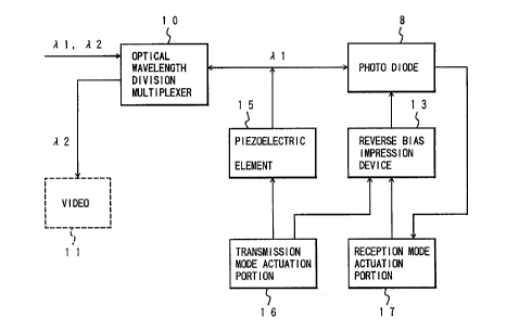
In Fig.1, the construction of major parts of one preferred
embodiment of an optical integrated circuit for
bidirectional communications according to the invention is
illustrated, using a block diagram. In Fig.2, an example of
the system configuration of optical transmitter-receiver
equipment 5 using the optical integrated circuit is
illustrated. As shown in Fig.1, an optical integrated
circuit for bidirectional communications of the preferred
embodiment is constructed of an optical wavelength division
multiplexer 10, a photo diode 8, a piezoelectric element 15,
a reverse bias impression device 13, a transmission mode
actuation portion 16, and a reception mode actuation portion
17.
CA 02211760 1997-07-30
. Doc.No.FP389 Patent
Furthermore, as shown in Fig.2, an optical waveguide
circuit 20 is formed by forming a lower clad layer 27a, core
18 and upper clad layer 27b on a substrate 25 in the order,
wherein a fiber fixing member 21 is secured at the incident
side of the optical waveguide circuit 20 as in the
conventional examples, and optical fibers 23a and 23b are
disposed and fixed at the fiber fixing member 21. On the
other hand, a photo diode 8 which acts as a semiconductor
light reception element is connected to the outgoing end 29
side of the core 18 of the optical waveguide circuit 20 and
is mounted on the substrate 25. A high reflection coating
film 30 which functions as a reflector of communication
signal light is provided at the photo diode 8. Furthermore,
a piezoelectric element 15 which acts as a polarization
plane modulating element is formed on the surface of the
upper clad layer 27b at the upper side at the outgoing end
29 side of the core 18.
The optical waveguide circuit 20 has a bidirectional
light input/output port 33 into which both communication
signal light of wavelength ~1 and non-communication signal
light (wavelength ~2) having a different wavelength from the
communication signal light, a communication light output
port 34 for leading only the communication signal light of
the communication signal light and non-communication light
which are made incident from the bidirectional light
input/output port 33 to the input side of the photo diode 8
and a non-communication light output port 35 for leading the
non-communication light in a direction deviating from the
input side of the photo diode 8, thereby constituting an
optical wavelength division multiplexer 10 shown in Fig.1.
The bidirectional light input/output port 33 is connected to
22
CA 02211760 1997-07-30
Doc.No.FP389 Patent
the optical fiber 23a, the communication light output port
34 is connected to the photo diode 8, and the non-
communication light output port 35 is connected to the
optical fiber 23b.
Furthermore, a main light path 52 which connects the
bidirectional light input/output port 23 and communication
light output port 34 is formed, and the non-communication
light output port 35 is provided at the outgoing end side of
a branch path 53 which is branched from the main light path
52, wherein a filter groove 22 is formed at the branch
portion where the main light path 52 and branch path 53 are
separated from each other, and a communication light
selective transmission filter 24 is provided at the filter
groove 22. The communication light selective transmission
filter 24 has functions of transmitting the communication
signal light incident from the bidirectional light
input/output port 33 to the communication light output port
34 side, transmitting the reflected light of the photo diode
8 of the communication signal light to the bidirectional
light input/output port 33 side, and reflecting the non-
communication light incident from the bidirectional light
input/output port 33 to the branch path 53 side.
Furthermore, in the preferred embodiment, a substrate
25 is made of silicon substrate, and the optical waveguide
circuit 20 is formed by any one of flame deposition method,
evaporation method, and chemical vapor phase growth method.
The abovementioned piezoelectric element 15 is, in this
preferred embodiment, constructed by laminating and forming
a lower electrode, a piezoelectric member, and an upper
CA 02211760 1997-07-30
Doc.No.FP389 Patent
electrode in the order on the surface side of the
abovementioned upper clad layer 27b. In detail, an Au/Cr
multilayered film is deposited as the lower electrode, ZnO
is formed to be film-like as a piezoelectric member by using
S a high-frequency magnetron spattering apparatus thereon, and
furthermore, an Au/Cr multilayered film is formed thereon as
the upper electrode by the same deposition method as that
for the lower electrode.
Furthermore, it is necessary to orient the ZnO in C axis in
order to obtain a good piezoelectric film. Since the atomic
orientation of ZnO in C axis is well matched to the atomic
orientation of (111) plane of Au, it is possible to form a
good piezoelectric film by orienting Au in (111) plane.
Still furthermore, by depositing Cr as the undercoat of Au,
it is possible to increase the (111) plane orientation of Au
in addition to an increase of the adhesivity of Au to glass.
The photo diode 8 is mounted to the substrate 25 via an
electrode pattern 19. A reception mode actuation portion 17
which actuates the photo diode 8 in line with the
synchronization timing of reception when communication
signal light is inputted into the photo diode 8 through the
optical waveguide circuit 20 and causes the photo diode 8 to
receive the communication signal light is connected to the
photo diode 8 as shown in Fig.1. Furthermore, although not
illustrated in Fig.1, a light reception drive circuit and a
reception modulating circuit which are similar to those in
the conventional example are connected to the reception mode
actuation portion 17. A reverse bias impression device 13
which is similar to that of the conventional example is
connected to the photo diode 8, and the reception mode
CA 02211760 1997-07-30
Doc.No.FP389 Patent
actuation portion 17 is constructed so that the photo diode
8 is actuated by driving the reverse bias impression device
13 when communication signal light is inputted into the
photo diode 8.
The transmission mode actuation portion 16 reflects the
communication signal light to the incident side
(bidirectional light input/output port 33 side) of the
optical waveguide circuit 20 by the high reflection coating
film 30 without actuating the photo diode 8 when the
communication signal light is inputted into the photo diode
8, simultaneously gives a polarization plane modulation to
the reflected light of the communication signal light by the
abovementioned piezoelectric element 15, and transmits the
polarization plane modulated light into the incident side
(bidirectional light input/output port 33 side) of the core
18 of the optical waveguide circuit 20 as transmission
light. With respect to this control, the transmission mode
actuation portion 16 is constructed so that the same
establishes a bias-free or a forward bias state by stopping
the reverse bias drive of the reverse bias impression device
13 when the communication signal light is inputted into the
photo diode 8 and the communication signal light inputted
into the photo diode 8 is transmitted (guided) from the
input side of the photo diode 8 to the high reflection
coating film 30 side.
Fig.5A and Fig.5B respectively show the detailed
construction example of the photo diode 8, wherein Fig.5A
shows a waveguide type light reception element and Fig.5B
shows a plane type light reception element. In these
drawings, 36 is a low reflection coating portion, 38 is an
CA 02211760 1997-07-30
Doc.No.FP389 Patent
upper electrode, 39 is a lower electrode, 40 is a p-InGaAs
contact layer, 41 is an InP ridge, 42 is a p-InP upper clad,
43 is a 1-InGaAs P core layer, 44 is an N-InP lower clad, 45
is non-reflection coating, 46 is a 1-InGaAs contact layer,
47 is an InP upper clad, 48 is a multiple quantum well, 49
is a black reflection mirror, and 50 is an InP lower clad.
For example, a waveguide type light reception element
shown in Fig.5A has such a laminated structure where a 1-
InGaAs P core layer 43 is put between the n-InP lower clad
44 and p-InP upper clad 42, thereby forming a PN junction
diode. In this photo diode 8, the low reflection coating
portion 36 is formed at the incident side of light and a
high reflection coating film 30 is formed at the opposite
IS side thereof, wherein as reverse bias impression voltage is
impressed from the reverse bias impression device 13 to the
photo diode 8, the same can be detected as an optical
current in response to the modulation of the incident light
(communication signal light) passing through the 1-InGaAs P
core layer 43.
Furthermore, in a case of a bias-free state where no
reverse bias voltage is impressed in the photo diode 8, the
1-InGaAs P core layer 43 becomes almost transparent.
Therefore, as a bias-free state is established by stopping
the drive of the reverse bias impression device at the
abovementioned transmission mode actuation portion 16 when
communication signal light is transmitted, the communication
signal light which is made incident into the photo diode 8
arrives at the high reflection coating film 30 through the
1-InGaAsP core layer 43, where the same is reflected by the
high reflection coating layer 30.
26
CA 02211760 1997-07-30
Doc.No.FP389 Patent
Furthermore, in a case of a plane type light reception
element shown in Fig.5B, the multiple quantum well 48
functions like the 1-InGaAsP core layer 43 of the waveguide
type light reception element shown in Fig.5A, and the photo
diode 8 is detected as an optical current in response to the
modulation of the incident communication signal light when
reverse bias voltage is impressed by the reverse bias
impression device 13, and when the bias-free state is
established, the incident communication signal light arrives
at the Bragg reflection mirror 49 through the multiple
quantum well 48, wherein the same is reflected by the Bragg
reflection mirror 49.
The preferred embodiment is constructed as described
above, and when an optical integrated circuit for
bidirectional communications is produced, for example, an
optical waveguide circuit 20 is formed at areas other than
the areas excepting the areas where the photo diode 8 is
disposed on the substrate 25, and an electrode pattern 19 is
formed on the surface side of the areas, at which the photo
diode 8 is disposed, at the substrate 25. Thereafter, by
mounting the photo diode 8 on the electrode pattern 19 and
connecting the same at the outgoing end 29 side of the core
18 of the optical waveguide circuit 20, an optical
integrated circuit for bidirectional communications can be
produced.
Next, a description is given of the actions of the
preferred embodiment. Furthermore, this embodiment is, for
example, installed at a subscriber house 2, as well as the
conventional optical transmitter-receiver equipment 5,
, CA 02211760 1997-07-30
Doc.No.FP389 Patent
wherein an optical fiber 23a is connected to an optical
fiber transmission cable 3 of an optical transmission system
for subscribers as shown in Fig.6 while an optical fiber 23b
is connected to a picture signal light reception device such
as a video 11, etc. And as communication signal light of
wavelength fÉ1 and picture signal light ~2 which are
transmitted by the optical fiber transmission cable 3 and
passes through the optical fiber 23a are made incident from
the bidirectional light input/output port 33 of the optical
waveguide circuit 20, the communication signal light and
picture signal light are made incident into a communication
light selective transmission filter 24, wherein the
communication signal light of wavelength fÉ1 is transmitted
through the communication light selective transmission
filter 24 and advances to the communication light output
port 34 side while the picture signal light of wavelength ~2
is reflected by the communication light selective
transmission filter 24, advances to the non-communication
light output port 35 side and is further received by the
video 11, etc. via the optical fiber 23b.
The communication signal light propagated to the
communication light output port 34 side is caused to exit
from the outgoing end 29 side and is inputted into the photo
diode 8. However, at this time, at the reception mode for
receiving communication signal light by the photo diode 8,
the photo diode 8 is driven by the reverse bias impression
device 13, which is carried out in response to the
synchronization timing of reception on the basis of control
of the reception model actuation portion 17 when the
communication signal light is inputted into the photo diode
8, whereby the communication signal light is received by the
28
, CA 02211760 1997-07-30
Doc.No.FP389 Patent
photo diode 8. This reception signal is demodulated by a
reception demodulation circuit secured at the reception mode
actuation portion and is detected as an optical current.
On the other hand, at the transmission mode which is
able to transmit communication signal light from the optical
integrated circuit for bidirectional communications, the
drive of the reverse bias impression device is obstructed by
the transmission mode actuation portion 16, whereby the
photo diode 8 is not actuated. Therefore, the communication
signal light inputted into the photo diode 8 by a station 1
side is allowed to reach the high reflection coating layer
30, wherein the communication signal light is reflected by
the high reflection coating layer 30 to the bidirectional
input/output end side of the optical waveguide circuit 20.
Furthermore, at this time, high-frequency signals are
impressed as transmission signals by the transmission mode
actuation portion 16, using a piezoelectric element 15,
whereby elastic waves are generated by a piezoelectric film
of the piezoelectric element 15, the elastic waves operate
on the core 18 to cause birefringence to be produced at the
core 18. Accordingly, with this action, polarization plane
modulation is given to the reflected light of the
communication signal light, wherein the polarization plane
modulated light is constituted to be transmission light
which is able to pass through the core 18 and pass through
the communication light selective transmission filter 24.
Herein, the modulated light reversely moves to the
bidirectional light input/output port 33 side and is
transmitted by the light fiber transmission cable 3, passing
through the optical fiber 23a, whereby the light
transmission is thus carried out.
29
CA 02211760 1997-07-30
. Doc.No.FP389 Patent
Furthermore, since the transmission light is made
polarization plane modulated light, the polarization plane
modulated light is caused to pass through an optical
s detector, etc. at the light reception portion ~for example,
station 1 side) of the transmission light to demodulate the
same as intensity modulated light, and the same can be
detected.
According to the preferred embodiment, by the
abovementioned actions, it is possible to carry out light
transmission by utilizing communication signal light
transmitted from the station 1 side without using any light
emitting elements such as laser diodes 6, etc. which are
IS requisite in the conventional light transmitter-receiver
equipment 5, and it is possible to carry out bidirectional
communications of light using the photo diode 8 which acts
as a semiconductor light reception element. Therefore, it is
possible to achieve the downsizing of facility and a
decrease of the production cost in line with omission of
light emitting elements such as laser diodes 6, etc.
Furthermore, as in the conventional example, in a case
where communication signal light is transmitted by using
light emitting elements such as laser diodes 6, etc., it is
necessary to emit intensive light which is caused to
transmit through an optical fiber transmission cable 3.
Therefore, a large-sized and highly accurate light emission
drive circuit is required. However, according to the
preferred embodiment, communication signal light is given
polarization plane modulation by utilizing the communication
signal light transmitted, for example, from the station 1
, CA 02211760 1997-07-30
Doc.No.FP389 Patent
side to a subscriber house 2 side and received by the photo
diode 8 in order to cause the same to be transmission light
from the subscriber house 2 side. Therefore, it is needless
to say that no large-sized drive circuit is required, and
the transmission light can be easily formed by the
polarization plane modulation of the communication signal
light received by the photo diode 8 side. Accordingly, it is
possible to easily obtain light transmission from subscriber
houses 2 side at a decreased production cost.
Furthermore, according to the preferred embodiment, in
addition to the downsizing and high integration of the
facility, and decrease of the production cost in line with
omission of light emitting elements such as laser diodes 6,
etc. and light emission drive circuit 12, which are
requisite in the conventional optical transmitter-receiver
equipment 5, only the photo diode 8 may be aligned with and
optically coupled to the optical waveguide circuit 20,
differing from the conventional optical transmitter-receiver
equipment 5 for which the laser diode 6 and photo diode 8
must be individually aligned and optical coupled to the
optical waveguide circuit 20. Therefore, the alignment work
and optical coupling thereof can be easily carried out in a
short time.
2s
Still furthermore, since the mode field diameter of the
photo diode 8 is not greatly different from the mode field
diameter of the core 18 of the optical waveguide circuit 20
unlike the mode field diameter of laser diode 6, the optical
coupling loss will not be increased unlike the optical
coupling between the laser diode 6 and the optical waveguide
circuit 20 in the conventional equipment. Furthermore, no
CA 02211760 1997-07-30
Doc.No.FP389 Patent
countermeasure against reflection is required in order to
prevent the optical coupling loss from being increased.
Therefore, it is possible to produce equipment. Resultantly,
the production cost of the equipment can be further
decreased.
Furthermore, according to the preferred embodiment, a
polarization plane modulating element to give polarization
plane modulation to the reflection light at the photo diode
8 with respect to communication signal light is formed of
piezoelectric elements 15. Since it is possible easily form
the piezoelectric elements 15 at a high accuracy by
laminating and forming a lower electrode, a piezoelectric
member and an upper electrode in the order on the surface
side of the upper clad layer 27b of the optical waveguide
circuit 20, the equipment can be further easily produced,
and it is possible to produce highly accurate equipment.
Furthermore, according to the preferred embodiment,
since Au/Cr multiple layers are used as a lower electrode
and an upper electrode when forming the piezoelectric
element 15, the Au glass adhesivity can be increased by
depositing Cr as the undercoat of Au, and the (111) plane
orientation of Au can be improved. Still furthermore, the C
axis orientation of ZnO can be performed by depositing and
forming a ZnO piezoelectric member at the lower electrode of
Au/Cr. Moreover, by giving polarization plane modulation to
the reflection light of the communication signal light using
the piezoelectric element 15, the polarization plane
modulation can be further accurately carried out.
CA 02211760 1997-07-30
. Doc.No.FP389 Patent
Furthermore, the present invention is not limited to
the preferred embodiment. Various variations and
modifications may be available as embodiments thereof. For
example, in the abovementioned preferred embodiment,
although an optical waveguide circuit 20 is constructed by
forming a lower clad layer 27a, a core 18 and an upper clad
layer 27b on the surface side of a substrate 25 in the
order, the surface of which is flat, for example, as shown
in Fig.3, the optical waveguide circuit 20 may be
constructed by forming a lower clad layer 27a on a substrate
25 having a dent portion 28 and forming a core layer 18 and
an upper clad layer 27b thereon.
Still furthermore, although in the above preferred
embodiment an electrode pattern 19 is directly formed on the
surface side of a substrate 25 and a photo diode 18 is
mounted on the electrode pattern 19, for example, as shown
in Fig.3, the photo diode 18 may be mounted on an electrode
pattern 19 which is formed on the upper side of an
insulation film 26 formed on the surface side of the
substrate 25 as necessary.
Furthermore, with the abovementioned preferred
embodiment, the optical waveguide circuit 20 has a main
light path 52 and a branch path 53 and provides a
communication light selective transmission filter 24 at the
branch portion of the main light path 52 and branch path 53,
and accordingly an optical wavelength division multiplexer
10 is formed, which is able to divide the communication
signal light and non-communication signal light incoming
from the bidirectional light input/output port 33 and leads
the communication signal light to the communication light
CA 02211760 1997-07-30
, Doc.No.FP389 Patent
output port 34 side and leads the non-communication light to
the non-communication light output port 35 side. However,
for example, as shown in Fig.4, the optical waveguide
circuit 20 may be a Mach-Zehnder interferometer type circuit
having the first optical waveguide 7a and second waveguide
7b.
Furthermore, the Mach-Zehnder interferometer type
circuit is such that the first waveguide 7a and second
waveguide 7b are juxtaposed and formed in a row with a gap
secured therebetween, two directional couplers 54 which are
formed with the first optical waveguide 7a and second
optical waveguide 7b approached each other partway of the
first optical waveguide 7a and second optical waveguide 7b
are arranged in series, and a phase-shifting portion in
which the length of the first optical waveguide 7a and that
of the second optical waveguide 7b are made relatively
different from each other is caused to intervene between the
two directional couplers 54. And in the example shown in
Fig.4, the incident side of the second optical waveguide 7b
is made a bidirectional light input/output port 33, and the
outgoing side thereof is made a communication light output
port 34 while the outgoing side of the first optical
waveguide 7a is made a non-communication light output port
35.
Furthermore, when a Mach-Zehnder interferometer type
circuit is used for an optical wavelength division
multiplexer 10 composed of an optical waveguide circuit 20,
the incident side of any one of the first and second optical
waveguides may be made a bidirectional light input/output
port, the outgoing side of any one of the first and second
34
, CA 02211760 1997-07-30
, Doc.No.FP389 Patent
waveguides may be made a communication light output port,
and the outgoing side of the other optical waveguide may be
made a non-communication light output port.
Furthermore, in the abovementioned preferred
s embodiment, although the piezoelectric element 15 is
constructed by laminating and forming a lower electrode of
Au/Cr, a piezoelectric member of ZnO, and an upper electrode
of Au/Cr in the order on the surface side of the upper clad
layer 27b of the optical waveguide circuit 20, it is not
necessary that the formation method of the piezoelectric
element 15 and materials used for forming the piezoelectric
element 15 are particularly limited, they may be adequately
determined.
lS Still furthermore, in the above preferred embodiment,
although a polarization plane modulating element which gives
polarization plane modulation to the reflection light at the
photo diode 8 of communication signal light is formed of a
piezoelectric element 15, the polarization plane modulating
element may not be necessarily limited to the formation by a
piezoelectric element 15. The same may be any element which
is able to modulate the plane of polarization with respect
to the reflection light of the communication signal light.
Furthermore, in the above preferred embodiment,
although the substrate 25 is a silicon substrate, the
substrate 25 is not limited to a silicon substrate. It may
be made of silica glass substrate.
Furthermore, in the abovementioned preferred
embodiment, although the optical waveguide circuit 20 is
formed by any one of flame deposition method, evaporation
, CA 02211760 1997-07-30
Doc.No.FP389 Patent
method, and chemical vapor phase growth method, the optical
waveguide circuit 20 may be formed by a method other than
these.
Furthermore, although in the preferred embodiment the
transmission mode actuation portion 16 causes the photo
diode 8 to enter a bias-free state by stopping the drive of
a reverse bias impression device 13 when communication
signal light is inputted into the photo diode 8 and causes
the photo diode 8 not to be operated, the transmission mode
actuation portion 16 may cause the reverse bias impression
device 13 to enter a forward bias state by stopping the
drive of the reverse bias impression device 13, thereby
causing the photo diode 8 not to be operated.
Furthermore, in the preferred embodiment it is
constructed that the optical waveguide circuit 20 is made a
circuit of the optical wavelength division multiplexer 10,
for example, wherein communication signal light of
wavelength ~1 and non-communication signal light (for
example, picture signal light of a wavelength ~2) of a
wavelength different from the wavelength of the
communication signal light is inputted into the
bidirectional light input/output port 33, only the
communication signal light is outputted from the
communication light output port 34 (the output end 29 of the
core 18) and is inputted into the photo diode 8 while the
non-communication light is outputted from the non-
communication light output port 35. However, the optical
waveguide circuit 20 provided in an optical integrated
circuit for bidirectional communications according to the
36
CA 02211760 1997-07-30
Doc.No.FP389 Patent
invention may not be necessarily limited to the circuit of
an optical wavelength division multiplexer 10.
For example, the optical waveguide circuit 20 may be
constituted to be a circuit having a core 18, communication
signal light inputted into a semiconductor light reception
element such as a photo diode 8, etc. through the core 18 is
received by the semiconductor light reception element by
controlling the reception mode actuation portion 17, and
communication signal light is reflected to the optical
waveguide circuit 20 side by controlling the transmission
mode actuation portion 16, wherein polarization plane
modulation is given to the reflection light to form
transmission light, and thereby is transmitted to the
incident side of the core 18 (that is, the bidirectional
light input/output end side).
However, when an optical integrated circuit for
bidirectional communications according to the invention is
applied to a subscriber light transmission system as shown
in Fig.6, if it is possible to receive both communication
signal light and non-communication light such as picture
signal light, etc. as in the abovementioned preferred
embodiment wherein communication can be carried out by only
the communication signal light and the picture signal light
can be introduced to a picture signal light receiving device
such as a video 11, etc., a system which can provide both
services of communication by communication signal light and
picture signal transmission by picture signal light by
utilizing an optical fiber transmission cable 3 can be
constructed at a decreased production cost.