Note: Descriptions are shown in the official language in which they were submitted.
CA 02211834 1997-07-2~
w~s6/24~7s PCT/AU96100048
-- 1 --
~ROADBAND GRATING
FIELD OF THE I~v~NllON
This invention relates to broadband Bragg gratings
and to a method of forming the gratings. The invention
has particular application to in-fibre Bragg gratings and
is hereinafter described in the context of a germano-
silicate fibre, having a photosensitive core, but it will
be understood that the invention does have broader
application, fc~r example to planar wave guides and other
light transmitting devices in which gratings may be
formed.
BACKGROUND OF THE INVENTION
Bragg grcLtings are conventionally employed as
filters in opt:ical commlln;cation systems. The gratings
are formed witkL regions of differing (i.e., high and low
amplitude) reEractive index in the direction of light
propagation and they reflect light over a spectral range
~AB centred on a wavelength ~B = 2nP where
~B = Bragg (centre) wavelength,
n = effective (average) refractive index, and
P = grating period.
The spectral region or bandwidth ~B over which
reflection occurs depends upon the strength of the
grating (i.e., the amplitude or depth of refractive index
modulation) and the length of the grating. In the case
of a 10 cm long grating that is formed to provide a
centre wavelength ~B ~f 1.55 ~m, the reflection bandwidth
would be in the order of 0.01 nm.
The above described Bragg gratings are employed
conventionally as optical filters which, in being formed
within optical Eibres, exhibit low insertion loss, and as
transducers in strain or temperature responsive sensor
devices. Also the gratings when chirped are employed as
dispersion compensators and function as such to reflect
different spectral components of light from different
axially spaced positions along the length of the grating.
Chirping has the effect of expanding the width of
the reflection peak and is achieved by varying the
CA 02211834 1997-07-2~
IAU~CI~C~8
WO 96/24079
-- 2
periodicity of the grating in the direction (Z) of light
propagation. The chirping may be linear in which the
grating period P = PO t ~Z or non-linear in which case
the grating period p = pO + ~zn for example.
One problem that is inherent in the above described
gratings, inc:luding those that are chirped to exhibit an
expanded speclral width, is that they cannot be tuned to
a significant extent. However, it would be useful if a
broa~band grat:ing of the described type could be produced
for use in processing a single channel signal to
facilitate a reduction in the degree of tuning required
to match a source to the grating. This in turn would
facilitate replacement of one source with another without
there being a need for critical component matching.
Another problem that is inherent in the known gratings is
that they cannot be employed singly to perform filtering,
dispersion compensation or other ~unctions simultaneously
on multiple channels at different wavelengths. In this
respect it has been recognised by the inventors that it
would be useful if a single grating could be employed to
perform equivalent fu~ctions on multiple cnmml~n;cation
channels such as exist in wavelength division
multiplexing (I~M) systems.
SUMMARY OF THE INVENTION
The present invention seeks to meet the above
stated needs by providing a light transmitting device
that comprises a Bragg grating which is formed in the
direction of ]ight propagation with grating regions of
alternatingly high and low refractive index, the grating
regions having periodicity P. Also, the grating regions
are structured in a manner which varies periodically with
a modulation period L ~ P, and either one or the other or
both of the gr~ting period P and the modulation period L
is or are chirped over substantially the full extent of
the grating.
The invention may also be defined in terms of a
method of producing a broadband Bragg grating and which
comprises forming grating regions of alternatingly high
CA 02211834 1997-07-2~
W O 96/24079 PCT/AU96100048
-- 3
and low refractive index in the light transmitting
device, the gra.ting regions being formed in the direction
of light propagation and having periodicity P. When
! forming the grating regions they are structured in a
manner which varies periodically with a modulation period
L ~ P, and chirping is imposed on either one or the other
or both of the grating period P and the modulation
period L over substantially the full extent of the
grating.
10The light transmi~ting device in which the grating
is formed may comprise any device in which regions of
differing refractive index may be created, but it
preferably comprises an optical fibre.
The grating regions may be structured in a manner
such that the amplitude and/or the phase and/or the
periodicity o~ the grating regions is/are varied
periodically (with modulation period L) along the length
of the grating. That is, in one embodiment of the
invention the a~mplitude of the high levels of refractive
index may be modulated, whilst in a second embodiment of
the invention t:he phase- may be varied by introducing at
least one discontinuity into each of the successive
modulation periods. In a third embodiment of the
invention, the periodicity of the grating regions may be
varied within each successive modulation period L, in the
manner of a sampled grating. In all three of the
identified embodiments, the complete grating is chirped
in terms of one or the other or both of the grating
period P and the modulation period L. Thus, chirping of
the complete grating is effected in addition to (i.e., at
the same time as or subsequent to) the establishment of a
periodic structure within the grating.
The grating period P will not be constant
throughout the length of the grating and will vary due to
chirping of the grating if for no other reason. However,
the grating period P will not vary by a significant
amount relative to the modulation period L and may be
considered notionally as having a substantially constant
CA 02211834 1997-07-2~
W 096/24079 PCT/AU~r'~ ~18
-- 4
value P < ~.
In the case of a grating in whicn the periodicity
o~ the grating regions is varied periodically, the
grating may be considered as one in which each of the t
successive portions (i.e., periods) of the grating is
structured as a chirped grating portion, with each 03 the
successive portions being substantially identical and,
but for chirping of the full grating length, having the
same phase relationship.
A grating in which the phase is varied periodically
may be achievecl by introducing at least one discontinuity
into each o~ the successive portions of the length of the
grating, such as by interrupting the sequence o~
alternating hiqh-low regions of refractive index in the
direction of light propagation.
In the case of a grating in which the high level o~
the re~ractive index is varied periodically as to
amplitude, modulation of the amplitude may be in the form
of a smooth wave function, for example as a sine wave
having a period L, or as a sawtooth wave~orm, but it
pre~erably is applied as a square-wave function. The
modulation may be partial or be applied for the full
re~ractive index depth of the grating regions, and in the
latter case would effectively create spaced-apart grating
sections. This effect may be achieved by forming
separate (periodic) grating sections, the sections being
spaced apart i3'L the Z direction and having period I, but
it would be essential in such case to ensure that a
constant phase relakionship is maintained between the
grating regions in the successive grating sections. This
may, for example, be achieved by side-writing a length of
grating by using W radiation and a single phase mask
- which extends for the full length of the intended
grating, and by discontinuing the writing o~ the grating
during alternating periodic intervals along the Z
direction 03- the mask.
The grating period P will typically be in the order
of 0.20 to 0.6() ~m, so that the reflected wavelengths
CA 02211834 1997-07-2~
wos6l24o7s PCT/AU96/00048
-- 5
will be in the range of 0.58 ~m to 1.74 ~m. The
modulation period L will typically be in the order of
0.20 to 8.00 ~n and most pre~erably will be in the order
of 1.0 mm. When the amplitude of refractive index of the
grating is 100~, modulated by a square wave o~ period L to
create spaced-apart grating sections, each grating
section may have a length in the direction of light
propagation in the order of 0.02 to 4.00 mm and
preferably in the order of 0.1 mm.
As statecL in the above definitions of the present
invention, either or both of the grating period P and the
modulation period L may be chirped, to produce different
spectral responses. If the grating period P is chirped
and the modulation period L is maintained constant (other
than to the extent that it may be influenced to a small
extent by chirping of the grating regions), the grating
will exhibit a spectral response in which identical
expanded (i.e., "chirped") reflection peaks having a
spectral width ~ appear at each side o~ an expanded
("chirped") reflection peak that is centred on the Bragg
wavelength ~B and fall _under an envelope determined by
the Fourier transform of the periodic modulation
function. The expanded reflection peaks at each side of
the centre wavelength will be spaced apart from the
centre reflection peak and from each other by the
distance ~A.
In an alternative grating in which the grating
period P is maintained constant and the modulation
period L is chirped, the grating will exhibit a spectral
response in which non-identical expanded ("chirped")
re~lection peaks having respective spectral widths ~
appear at each side of a narrow reflection peak centred
on ~B and having spectral width ~B~
In the further alternative form of the grating, in
which both the grating period P and the modulation
period L are ch:irped, the grating will exhibit a spectral
response in which non-identical expanded ("chirped~)
reflection peaks having respective spectral widths
CA 02211834 1997-07-2~
W O 96/24079 PCTlA~-g~ 18
-- 6
appear at each side of an expanded ("chirped") reflection
peak having spectral width ~ centred on ~B-
Chirping of the grating period P and the modulationperiod L may be effected in any known manner, for example
during side-writing o~ the grating or, following writing
of the grating, by subjecting the grating to a post-
formation chirping procedure as known in the art. Thus,
chirping may be achieved by application of strain
differentially along the length of the grating, by
applying loading to a previously tapered ~ibre core, by
application o~ heat to establish a temperature gradient
along the lengt:h of the grating or by modification of the
structure o~ the grating by applica~ion o~ any one of the
known techniques for inducing the stress optic effect.
The grating as above defined may be structured
further by varying the amplitude o~ the high levels of
refractive index over the full length of the grating, in
addition to establishment of the periodic structure. For
example, a Gaussian envelope may be imposed on the
grating regions over the full length of the grating for
the purpose of smoothing the spectral response.
The grating in its various possible forms may be
used in various optical circuits, ~or example to provide
for dispersion compensation at multiple wavelengths.
Thus, the invention may be defined further as
providing an optical commlln;cation system comprising an
optical transmitter which is arranged to transmit light
having a centre wavelength ~ and bandwidth ~, a receiver
arranged to receive the transmitted light, and a light
transmitting medium connecting the transmitter and the
receiver. A grating of the type as above defined, which
exhibits multiple reflection peaks, is located in circuit
with the light transmitting medium and the grating is
selected such that one of its reflection peaks has a
centre wavelenqth that coincides with the transmitter
wavelength ~ and has a bandwidth at least equal to the
bandwidth ~.
In the above de~ined system the wavelength of a
-
CA 02211834 1997-07-2~
wos6/2407s PCTIAU96/00~8
-- 7
replacement light source may effectively be tuned to that
of the r~m~;n~er of the system, provided that the amount
of tuning required is not greater than one-hal~ of the
spectral separation between the reflection peaks of the
grating. .
In a part:icular application of the invention, the
above defined optical c~mml-n;cation system may comprise
an optical transmitter which is arranged to transmit
multi-channel l.ight having centre wavelengths ~l'~~~~~n
and channel band widths ~ a receiver arranged
to receive t:he ~ransmitted light, and a light
transmitting medium connecting the receiver and the
transmitter. .~ grating of the type as above defined,
which exhibits multiple reflection peaks, is located in
circuit with the light transmitting medium and is
connected optically with means arranged to direct light
into the grating from a first portion of the light
transmission medium, to receive reflected light from the
grating and to direct the reflected light into a second
portion of the light transmitting medium. The grating is
selected such t:hat its reflection peaks coincide with the
centre wavelength ~ n and have spectral widths not
less than the respective channel bandwidths ~ n~
The invention will be more fully understood from
the following d.escription o~ three exemplary embodiments
of in-fibre Bragg broadband gratings and from the
description of a preferred method and apparatus for
producing the gratings within optical fibres. The
description i'3 provided with reference to the
accompanying drawings.
BRIEF DESCRIPTION OF THE DRAWINGS
In the dra.wings -
Figure,1 ~;hows on an enlarged scale a portion of anoptical fibre incorporating a grating in accordance with
a first embodiment of the invention,
Figure 2 shows a graphical representation of two
sections of the grating as shown in Figure 1,
Figure 3 shows on an enlarged scale a portion of an
CA 022ll834 l997-07-2
W 096/24079 PCT/AU~S/~C1
- 8
optical fibre incorporating a grating in accordance with
a second embodiment of the invention,
Figure 4 shows a graphical representation o~ two
sections of the grating shown in Figure 3,
Figure 5 shows on an enlarged scale a portion of an
optical fibre incorporating a grating in accordance with
a third embodiment of the invention,
Figure 6 shows a graphical representation of two
sections of the grating shown in Figure 5,
Figure 7 shows an apparatus used in side writing a
length of the c~ptical fibre shown in Figure 1,
Figure 8 shows an idealised graphical
representation of the spectral response of the grating
shown in Figures 1 and 2,
Figure 9 shows a graphical representation of the
spectral respo~lse of the grating shown in Figure 1, in
the plot A before chirping and in the plot B after
chirping, and
Figure 10 shows a block diagrammatic representation
of an optical commlln~cation system that incorporates one
or other of t.he gratings as represented in Figures 1
to 6.
DETAILED DESCRIPTION OF MODES OF THE INVENTION
The optical fibre 10 that "carries" the various
embodiments of the grating comprises a single mode boro-
germano-silicate fibre and when formed is loaded with
molecular hydrogen to increase its photosensitivity.
This is achieved by "soaking" the fibre in a highly
pressurised atmosphere of hydrogen at 70 atm at 70~C for
24 hours.
The grating is written into the optical fibre 10 in
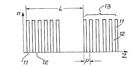
the direction of light propagation through the fibre and,
as shown in Figures 1 and 2, grating regions 11 and 12 of
alternatingly high and low refractive index are formed in
the optical fibre 10 with periodicity P. Also, the
grating regions 11 and 12 are structured in a manner such
that the amplitude of the high levels of refractive index
is varied periodically with a modulation period L. The
CA 02211834 1997-07-2~
W O 96/24079 PCTlAU96tO0048
g
modulation of the c~mplitude might take the ~orm o~ a
smooth wave ~unction or any other periodic form, but as
illustrated in Figures 1 and 2 a 100~ scluare wave
modulation is applied to the grating regions so as to
create spaced-apart grating portions or sections 13.
The grating period P will typically be in the order
of 0.20 to 0.60 ~m, depending upon the recluired
reflection wavelength, but will vary along the length of
the grating with chirping of the grating. The modulation
period will typically be in the order of 0.20 to 8.00 mm.
The length of each section 13 will typically be in the
order of 0.1 mm and the total grating length will
typically be in the order of 5 to 10 cm.
The grating 10 is chirped for its full length, by
chirping the grating period P, the modulation period L or
both the grating period and the modulation period. Which
of these chirps is imposed will be dependent upon the
spectral response recluired to be exhibited by the
grating, this having been described in more detail
earlier in the specification. Linear chirping is most
preferably imposed on the grating, typically in the order
o~ 0.03~.
The grating which is shown in Figures 3 and 4 of
the drawings is structured in a manner such that the
periodicity of the grating regions is varied periodically
with modulatian period L. Each of the grating
sections 13 incorporates grating regions 11 and 12 of
alternatingly high and low refractive index, but the
grating period P within each section 13 ~;m;n;shes
linearly with length of the grating section. Thus, each
grating section may be considered as being separately
chirped, typically in the order of 1.0~ to S.0~, in the
manner of a sample grating, but further chirping is
imposed on the grating over its full length.
The grating shown in Figures 3 and 4 will have a
no~;n~l grating period P in the order of 0.20 to 0.60 ~m
and will otherwise have ~;men~ional characteristics
similar to those which have been described above with
CA 02211834 1997-07-2~
wos6l2407s PCT/AU96/00048
- 10 -
reference to Figures 1 and 2.
The grating which is shown in Figures 5 and 6 o~
the drawings is structured in a manner such that the
phase is varied by a discontinuity in each of the
successive grat:ing sectlons 13. Each of the grating
sections 13 incorporates grating regions 11 and 12 of
alternatingly ]ligh and low refractive index, with a
grating period P, but a phase change is introduced by
interrupting the sequence of alternating high-low regions
of refractive index, for example by establishing
consecutive regions lla of high refractive index. Each
section of the grating is identical and the sections are
spaced by modulation period L.
The grating as shown in Figures 5 and 6 has
~;men~ional cha.racteristics similar to those described
above with reference to Figures 1 to 4.
Although the various grating configurations have
been described in the context o~ separate gratings, the
grating regions of any one grating may be structured in a
manner such that the amplitude and the phase, or the
amplitude and the peri~dicity, or the phase and the
periodicity are, in respective cases, both varied
periodically with modulation period L.
Each of t:he above described gratings is written
into the optical fibre 10 in the direction of light
propagation through the fibre and, whilst various
techniques may ]~e employed for side-writing the grating,
a phase mask 14 preferably is employed in the manner
indicated in Figure 7. The phase mask comprises a silica
mask having 1 mm long parallel grooves 15 which are
spaced apart with a period of 1.06 ~m, assuming that the
grating is to have a period P of 0.53 ~m to produce a
reflection peak centred on ~B ~f 1.55 ~um. The grooves
within the phase mask are etched to a depth of
approximately 240 nm, and the grooves extend over a
distance of 14 cm in the direction perpendicular to their
length and, thus, in the direction of propagation of
light through the grating. The phase mask 14 may be
CA 02211834 1997-07-2~
W O 96/24079 PCTIAU96/00048
- 11 -
employed to produce a grating having a 10 cm length and,
with the ~lm~n~ions stated, is arranged to diffract W
light at 240 nm mostly in the +1 and -1 orders of
di~fraction.
The fibre 10 is stripped of its protective coating
for a distance at least as long as the grating to be
written (10 cm as de.5cribed), and placed directly behind
the phase mask 14 such that the axis of the fibre is
perpendicular to the mask grooves 15. The fibre is laid
in V-grooves 16 and is held by magnets 17, so that it is
maintained under a slight tension.
A laser beam pulsed at 10 Hz, at a wavelength
of 240 nm is generated by a frequency-doubled excimer-
pumped dye laser 18 and is directed through a mechanical
shutter 19. The laser beam is deflected by a mirror 10
and focused by way of a fused silica cylindrical lens 21
which is locate~ with its axis perpendicular to the ~ibre
axis, in such a way that the beam width on the fibre
corresponds to the width of one section 13 of the
grating. The lens 21 has a focal length of 20 cm and the
lens is positioned at a-distance from the fibre selected
to determine the re~uired beam width.
The mirror 20 and lens 21 are both mounted to a
carriage 22 in such a way that they may be moved as a
unit in a direction parallel to the incident laser beam
and to the fibre axis. Thus, the focused, deflected beam
from the laser is translated along the fibre by movement
of the carriage 22 and is aligned in a way such as always
to be incident with the same power density on the core of
the fibre when the passage of the beam is unblocked by
the shutter 19.
When writing the grating, the carriage 22 is first
brought to rest in a desired position and the laser beam
is passed through the shutter 19, so that a short section
of the grating is written into the fibre as a consequence
of the interference pattern created by the diffracted W
beam. The pulse energy of the laser beam will typically
be in the order of 2 mJ, and the energy density impinging
CA 022ll834 l997-07-2~
W 096/24079 PCT/AU96/00048
- 12 -
on the fibre core will typically be in the order of
10 mJ/mm2. The strength, or depth of refractive index
modulation effected by the side writing is proportional
to exposure t:ime and a typical exposure time will be
around 10 to 50 seconds.
Following the required period of exposure to
irradiation, the shutter 19 is closed to block the laser
bearn and the carriage 22 is moved by distance L, being
the period of ispaced-apart sections of the grating to be
written into the length of the fibre. As stated in the
preceding text, the distance L is significantly greater
than the period P of the grating itself and typically
will be in the order of 1.00 mm. In the case o~ a phase
mask which is etched to provide a centre Bragg wavelength
of 1.55 ~m, and where the effective refractive index of
the grating is 1.46 and the desired spectral separation
is 1.0 nm, the distance L will be O.812 mm by application
of the formula provided earlier in this text.
After forward movement of the carriage 22 the
shutter 19 is again opened to permit further irradiation
of the fibre and this- process is repeated until the
desired length of grating has been created.
Chirping of the period P of the grating and/or of
the modulation period L may be effected during formation
of the grating itsel~ by appropriately grooving the phase
mask 14. As an alternative approach, chirping may be
effected following formation of the grating, for example
by use of a procedure involving application of strain
differentially along the length of the grating.
Chirping in one or the other the manner described
is applied along the full length of the grating.
Figure 8 of the drawings shows an idealised
graphical representation of the grating that is shown in
Figures 1 and 2 and which is produced in the manner
described above with reference to Figure 7. The
graphical representation is applicable to a grating in
which the grating period P is chirped and the modulation
period L is maintained substantially constant. In this
CA 02211834 1997-07-2~
W O 96/24079 PCT/AU96/00048
- 13 -
case identical, expanded reflection peaks having a
spectral width ~ appear at each side of an expanded
reflection pea~: that is centred on the Bragg wavelength
~B~ with the spacing between the peaks being
In the case of a grating having a centre Bragg
wavelength ~B of 1.55 ~m and having a length in the order
o~ 10 cm, the grating will exhibit a spectral width ~AB
in the order of 0.01 nm and an e~An~ ("chirped")
spectral width ~ in the order of 0.5 nm, resulting ~rom
a linear chirp o~ 0.031~ applied to the grating period P
over the full length of the grating.
The centre spacing A~ between adjacent peaks in the
spectral responses may be shown to be A~ = ~B2/2 n~ and
typically will be in the order of 1.00 nm in the case of
a Bragg wavelength AB ~f 1.55 ~Lm and modulation period
L = 0.8 mm.
Figure 9 ~3hows a plot of transmission power against
wavelengths applicable to a grating that has been
fabricated in a hydrogen loaded, boro-germano-silicate
optical fibre. A 240 nm, 10 Hz, 2 mJ/pulse beam was
focused to a 0.15 mm width by a cylindrical lens with its
axis perpendicular to the ~ibre axis, in the manner
described with reference to Figure 7. The beam was
translated along the optical fibre, which was placed
directly behind a 14 cm long phase mask, and translation
was stopped every 1.0 mm to expose a region o~ the
optical ~ibre for 40 seconds. The total length of the
grating so produced was 100 mm and, although not shown in
Figure 9, the t:ransmission spectrum ~or the grating shows
plus strong re~lection peaks with bandwidth of
0.04 nm. The grating was chirped ~ollowing side writing
to produce a linear chirp in the order o~ 0.03~ along the
~ull length of the grating to broaden the reflection
peaks. Figure 9 shows a spectrum o~ three o~ the
strongest peaks be~ore and a~ter chirping and, apart from
some irregularit:ies, attributed to deviations from linear
chirp, the peak~; are seen all to be broadened to the same
bandwidth of 0.36 nm.
CA 02211834 1997-07-2~
W 096/24079 PCT/AU96100048
- 14 -
Figure 10 shows a block diagrammatic repre~entation
o~ a comml~n;cation system in which any one of the above
described gratings may be employed for the purpose of
processing multiple channels having separation ~ and
S spectral width not greater than ~. ~s illustrated, the
system includes an optical transmitter 25 in which multi-
rh~nn~l light outputs are generated with carrier
wavelengths Al,A2,~~~~An modulated to bandwidths
~ A2, ~~ ~ ~ ~n with system information. The output from
the transmitter 25 is launched into a first section of
what is referrel~ to generally as an optical transmi~sion
medium 26 which may include an optical fibre and such
other optical components as may be required, for example,
to connect, spl:it, filter or amplify the output from the
transmitter. A bro~h~nA grating 27 of a type as above
described is located in circuit with the transmission
medium 26 and the grating is selected such that it
exhi~its broad reflection peaks at wavelengths that
coincide with each of the carrier wavelength ~ 2l~~~l~n
and exhibits reflection peaks having bandwidths greater
than that of the bandwidths ~ 2~ n~ An optical
device 28, for example in the form of a circulator or
coupler, is located between the transmission medium 26
and the grating 27 for directing the transmitter output
into the grating, receiving reflections from the grating
and directing the reflected light into a ~ollowing
section of transmitting medium 29.
The above described arrangement is repeated as
required for a given system and two repeats of the system
are shown in ~'igure 10. The output from the final
section 30 of the transmission medium is fed to an opto-
electronic receiver 31.