Note: Descriptions are shown in the official language in which they were submitted.
CA 02211923 1997-07-30
l ~..
~ C ~; _
C% i..r~~$.~)::~~.; 01 t1
,t.: :~ y
rtitt~:.~ .~ r ~ i;:~
OPTICAL SYSTEM EMPLOYING NEAR-INCOHERENT
PROCESSING FOR DISTORTION CORRECTION
TECHNICAL FIELD
The present invention relates generally to systems for correcting
nonlinear distortion in fiber optic communication systems and more
particularly to an optical network that employs optical modulators and adds a
correction signal on a fiber optic cable.
BACKGROUND OF THE INVENTION
The use of electrooptic modulators for high dynamic range fiber
optic link applications in the communications field and in other applications
has been hindered by the nonlinearity of these devices. The Mach-Zehnder
modulator which is the work horse of the analog links, possesses an intrinsic
nonlinearity due to the interferometric nature of its operation. Linearization
of these devices has become necessary in the most demanding applications.
The linearization of electrooptic modulators for high dynamic range
applications has taken many forms.
Basically, there are two classes of linearization that have been
explored. The first class contains those devices having electronic
predistortion which electronically produces the correction for third order
distortion prior to feeding the signal into a modulator. This approach is
limited in its capacity to maintain the proper amount of correction over very
large signal applications where higher order nonlinearities occur. In
addition, the stability required in most applications is lacking and devices
incorporating the electronic predistortion are difficult to produce.
The other approach which has been explored on a limited basis
is founded on classic feed--forward techniques used in the design of high
performance, high frequency RF amplifiers for many years. In this approach,
the nonlinear element is t:he modulator and is driven directly by the
supplied RF signal. The output of this nonlinear element is then
electronically compared to the input, and an error signal is produced. The
error signal is simply the difference between the input to and output of the
nonlinear element. This error signal is then amplified, fed forward and
combined with the output: of the first nonlinear element. Care has to be
taken to match the amplitude and phase of the error signal and the original
output of the element in order to insure adequate cancellation of the error
A~ENDED SI"'I~E r SUBSTITUTE SHEET
IP~A/EP
CA 02211923 1997-07-30
L
signal.
Exemplary prior art is shown in reference D1, U.S. Pat. No.
5,166,509 to Curran shows an optical modulator noise nonlinearity reduction
circuit. An optical modulator or laser source 10 has a detector 14 for
detecting
its output signal, and producing a corresponding output signal. A tapping
device 12 is connected to tap off a portion of the input modulation signal as
a
reference signal, which is compared to and subtracted from the detector
output signal by a subtraction unit 18 to produce an error output signal
proportional to the laser noise/distortion components. The error signal is
amplified by amplifier 34 and fed to an external modulator, to reduce or
cancel the noise/distortion in the laser output signal.
Reference D2, U.S. Pat. No. 5,289,550 to Plastow shows a
modulated light source ~n~ith a linear transfer function and method utilizing
the same, including two rnodulatable optical sources. The output of the first
modulator, with a high power low noise, is sampled, compared to the input
signal, and used to generate an error signal used to modulate the second
optical source, with a low power and moderate noise. The output of the
second modulator is combined with a delayed output of the first modulator
to remove departures from linearity.
It would be desirable to have a system for correcting harmonic
distortion in fiber optic networks which is wavelength independent and
which allows the use of a single light source. The present system is drawn
towards such an. invention.
SUMMARY OF THE INVENTION
An object of the present invention is to provide an apparatus
for correcting nonlinear distortion by means of a feed-forward correction
apparatus in a fiber optic system having a single laser source.
Another objf:ct of the present invention is to provide an
apparatus of the foregoing type which alters the coherence of an optical
signal
by means of an optical phase modifying device such that stable feed-forward
correction is achieved wii:hout spurious interference signals within a
selected
radio frequency band.
Yet another object of the present invention is to provide an
apparatus of the foregoin~~ type in which the phase modifying device utilizes
SUBSTITUTE SHEET
!°~A~~P
i CA 02211923 1997-07-30
~~0.
a time dependent sine wave (or combination of sine eaves) variation of the
differential optical phase of the optical signals.
Still another object of the present invention is to provide an
apparatus of the foregoing type in which the phase modifying device
generates interference terns or noise outside of the radio frequency band.
Another object of the present invention is to provide an
apparatus of the foregoing type characterized by an optical delay of a source
within a limited temporal coherence to alleviate interference between the
combination of the main and corrective optical signals.
Another object of the present invention is to provide an
apparatus
AI~EI~~E ~ S;~EET
SUBSTITUTE SHEET
IPEA/E"
CA 02211923 2000-05-26
- 3 -
of the foregoing type characterized by orthogonal states
of polarization for the main and corrective optical
signals.
Still another object of the present invention is to
provide an apparatus of the foregoing type in which the
optimization of the feed-forward network is accomplished
via parametric control of optical and electrical
components.
According to the present invention, a system for
providing compensation for nonlinearities in an optical
system that transmits data signals in a data transfer
frequency band, includes an optical source for providing
a coherent main optical beam; a beam splitter for
receiving the optical beam and providing first and
second split optical beams; and a frequency generator
for generating a radio frequency (RF) modulation signal
whose frequency spectrum includes the data transfer
frequency signal band. There is an RF signal tap for
extracting a reference portion of the RF modulation
signal as well as a main modulator for receiving the RF
modulation signal and modulating the first split optical
beam to output a modulated main optical beam having
modulated and distorted optical components. A quasi-
incoherent compensation apparatus includes an
incoherence mechanism for making the second split
optical beam and the main optical beam incoherent with
respect to one another in the data frequency signal band
such that no optical interference products between the
main and the second split optical beams occur within the
data transfer frequency band when the main and the
second split optical beams are combined. There is also
a mechanism for generating an error signal indicative of
the difference between the RF signal and said distortion
portion of the main optical beam. A compensation
modulator modulates the second split optical beam in
accordance with the error signal. An optical combiner,
CA 02211923 2000-05-26
- 3a -
downstream of the incoherence mechanism and the
compensation modulator, receives the modulated main and
second split optical beams and provides therefrom a
compensated output beam.
BRTEF DESCRIPTION OF THE DRAWING
Fig. 1 is a simplified schematic representation of
a known optical system providing correction for
nonlinear distortion.
Fig. 2 is a simplified schematic representation of
a system providing optical correction for nonlinear
distortion as provided according to
CA 02211923 1997-07-30
WO 96/24201 PCT/US96/01334
4
the present invention.
Fig. 3 is a diagrammatic representation of modulated optical signals
including a signal as compensated by the system of Fig. 2
Fig. 4 is a diagrammatic representation of modulated optical signals
showing a composite triple beat measurement.
Fig. 5 is a simplified schematic representation of a first alternative
embodiment of the present invention utilizing phase delay.
Fig. 6 is a simplified schematic representation of a second
alternative embodiment of the present invention utilizing orthogonal states of
polarization.
Fig. 7 is a simplified schematic representation of an other
alternative embodiment of the present invention utilizing dithered servo
control of feed forward parameters.
Fig. 8 is a simplified schematic representation of still another
alternative embodiment of the present invention utilizing dithered servo
control with a pilot tone added to the main modulator.
Fig. 9 is a simplified schematic representation of another
alternative embodiment of the present invention utilizing active control of
relative signal gains.
Fig. 10 is a simplified schematic representation of another
alternative embodiment of the present invention generating two output beams.
CA 02211923 2000-05-26
DESCRIPTION OF THE PREFERRED EMBODIMENT
In a fiber optic link correction of harmonic
distortion can be accomplished through the use of a
known system similar to that shown in FIG. 1. In this
5 system 10, a laser 12 generates an optical signal 14 for
presentation to modulator 16. A radio frequency signal
generator 18 presents an RF signal on line 20 to the
modulator while a portion thereof is tapped off on line
22 for the generation of an error signal. This tapped
off portion of the RF signal is combined with a pick off
signal on line 24. The pick off signal is initially
produced by a detector 26 connected to an optical tap 28
on the output side of the modulator and thereafter
amplified by amplifier 29. A representation of the RF
spectral content of the signal generated by the signal
generator is shown at phase plot 30, while the phase of
the modulated optical signal is indicated at phase plot
32. In these plots, phase is indicated by the upward
pointing arrows.
This optical signal combination is performed such
that the result is the exact signal needed to correct
any errors in the modulator. An error correction signal
on line 34 is then used to drive a laser diode 36 which
will produce an optical signal indicated at 38 carrying
the error information. The output of the laser diode
whose relative phase is shown by the downward arrows of
plot 40 is then combined with the modulated optical
signal presented by the original modulator' through the
use of an optical tap 42. The resulting output signal 44
presented on the fiber is the original modulator output
co-propagating with the error signal. At the detector at
the end of the optical fiber (not shown), these two
signals are transformed into photocurrents which add;
thereby yielding the desired sum of the original signal
out of the modulator and the error signal. The resulting
sum should ideally be a signal resembling the original
CA 02211923 2000-05-26
5a
RF input.
This implementation is fraught with several
drawbacks. The foremost is the fact that the CW laser
source used for the modulator and the laser diode are of
differing wavelengths. This difference in wavelengths is
always great enough that the two signals do not
propagate on the fiber at exactly the same velocities
due to the dispersion of standard single mode fibers
used today. This difference in velocity gives way to
phase shear between the error and the signal as they
propagate down the fiber. After about 5-10 km of
propagation, the system is incapable of correcting the
nonlinear distortions of the modulator to
CA 02211923 1997-07-30
WO 96/24201 PCT/US96/01334
6
the degree typically needed (20dB). While it is conceivable that these can be
produced on the exactly the same wavelength, it is not practical.
A solution to this problem is to use the same laser source split two
ways, one for the main modulator and the other for a modulator used to
generate the optical error signal. In this arrangement, the laser diode of the
system of Fig. 1 is simply replaced with a modulator similar to the main
modulator. This would be acceptable if it were not for the fact that, at the
final
optical coupler, the main optical signal and error signal add coherently in
the
optical domain, producing cross terms which are not present in the system 10.
The cross terms are extremely sensitive to the relative phase of the two
optical
signals. A solution is achieved by accurately controlling the optical phase of
the
two beams, but such control is extremely difficult to accomplish to the degree
necessary.
Referring now to Fig. 2 , there is shown a system 45 provided
according to the present invention having a single wavelength feed-forward
topology which alleviates the coherent effects of combined beams. The present
invention provides, in essence, a system with a second optical beam source by
synthesizing the same from a portion of the system's laser beam. The main
requirement of the synthesized optical beam is that, when combined with the
system laser beam, the resultant beam produces no interference at frequencies
within the band of interest; i.e., the beams are quasi-incoherent. Several
embodiments of the present invention are detailed herein which manipulate
the optical phases of the main and synthesized "error" beams to produce the
quasi-incoherent combined beams with no deleterious spurious interference
terms within the needed frequency response of the overall optical system.
Techniques used in these embodiments include frequency shifting polarization
rotation and time delay. Feed-forward correction of nonlinear distortion
products is realized with a single laser source.
CA 02211923 2000-05-26
7
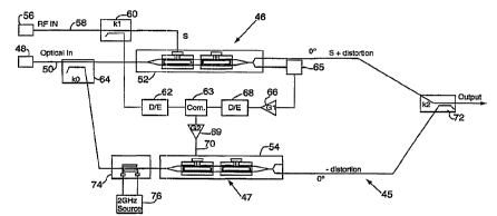
The system 45 can be divided into main and
correction optical circuits 46, 47. The main optical
circuit includes a laser 48 that provides an optical
beam 50 that functions as the optical carrier. There is
a first modulator 52 that is the "main" modulator, while
a second, "error correction" or feed-forward modulator
54 is also provided. A radio frequency generator 56
presents an RF signal on line 58 to the main modulator,
while a portion of that RF signal is extracted at tap 60
for presentation to delay and equalization circuitry 62
whose output is presented to a signal combiner 63.
A portion of the laser beam is also extracted by an
optical splitter 64 which presents the extracted optical
beam to the input of the correction modulator. A portion
of the main modulated optical beam is also tapped,
detected by photodetector 65 and amplified by amplifier
66 and presented first to delay and equalization
circuitry 68 and then to a second input port on the
combiner 63. A difference signal between the output of
the main modulator and the input signal thereto is
amplified by amplifier 69 and fed on line 70 to the
correction modulator. The two optical beams from the
main and correction modulators are then combined at
final optical coupler 72 to achieve cancellation of
nonlinear distortion products.
Problems arising from the interference between the
optical beams can be alleviated in the frequency band of
interest by appropriately modifying the differential
optical phase imposed by the main phase modulator. In
the feed-forward embodiment of FIG. 2, the error signal
is generated in a known manner and fed to the correction
modulator which generates the optical version of the
error. As noted, the optical beams arriving at the final
optical coupler are coherent in the RF and the optical
domains. With the present invention, the optical
CA 02211923 2000-05-26
7a
coherence of these fields is altered by phase modulator
74 which receives the extracted optical beam before
presentation to the correction modulator. The phase of
the extracted beam is changed to move the beam out of
band by the use of a single tone constant amplitude
signal such as a 2 GHz tone provided by phase modulation
signal generator 76. The alteration of the coherence of
the optical fields is done so as to produce no optical
interference between the two beams at the final optical
coupler at any frequencies within the desired bandwidth.
CA 02211923 1997-07-30
WO 96/24201 PCT/US96/01334
8
The simplest, but by no means the only way, to view the present
invention is to utilize a frequency shifting element in place of or, for the
present
purposes an equivalent of, the phase modulator. Examples of frequency shifting
elements could include accoustoptic devices or complex integrated optical
circuits for accomplishing the same. If the optical signal (carrier) entering
the
error modulator has a frequency offset relative to the carrier entering the
main
modulator, the resulting interference of the optical beams at the output
coupler
would occur at a frequency equal to this offset. The resulting photocurrent in
a
detector placed at the end of a fiber optic cable, for example, would contain
the
two signals, error and main, and an interference term which is around the
frequency offset. This can be expressed as
I out = S2 Main + S2 Error + F(SMain x SError) Eq. 1
Where lout is the photocurrent in the detector, SMain arid SE,ror are the
optical
field amplitudes from the main and error modulators respectively, and F is a
function of the product represented in its argument. It is in this function,
F, that
the interfering cross terms are recovered. As stated above however, the
frequency content of the signals represented by the function F would be
centered
around the frequency offset and out of the band of interest.
In the embodiment shown in Fig. 2, the phase modulator is used,
effectively, to frequency shift the optical carrier at a frequency greater
than twice
the bandwidth. In addition, if the phase modulator is driven such that the
peak
to peak phase deviation is equal to 2.405 radians (corresponding to Jp, the
first
zero of the Bessel function), the spectrum of the optical carrier signal
entering
the error modulator will posses energy at frequencies offset from the carrier
at
multiples of the driving frequency but none at the original carrier frequency.
In
this special case the carrier is said to be depleted. Thus, any optical
interference
between the error beam and the main beam will not produce any spurious
signals within the system's bandwidth, just as in the pure frequency shift
example set forth above.
While a simple phase modulation of the optical carrier beam has
been demonstrated, there are other waveforms which can accomplish the same
desired result. The possible waveforms which can be used to minimize the
coherent cross terms in Eq. 1 which give rise to in-band interference effects
can
be determined by noting the nature of the interference cross term given by F
and
CA 02211923 1997-07-30
WU 96!24201 PCTlUS96101334
9
proportional to a cosine function as shown below.
F(SxS,> ~ cos(cr(t)) Eq. 2
This implies that, in order to eliminate the effects of this term within the
RF
bandwidth of interest, e(t) must be chosen such that the time average of this
term is approximately zero.
cos(e(t)) = 0 Eq. 3
where the time average interval is comparable to the inverse of the highest
frequency in the RF band of interest. In practice this time interval must be
no
greater than the inverse of twice the highest frequency. There are a number of
solutions which satisfy this condition. A partial list is shown below.
~ Sine/cosine wave with amplitude 2.405 radians or any other
amplitude corresponding to a zero in J0.
~ Frequency modulated signal with amplitude 2.405 radians or any
other amplitude corresponding to a zero in J0.
~ A combination of harmonic signals.
~ Limited bandwidth random noise with the proper characteristics
so~ as to deplete the carrier.
Due to the one-to-one correspondence between the voltage applied to the phase
modulator and the induced phase shift, any solution to Eq. 3 can be realized
by
applying an electrical signal in the form of the solution directly to the
phase
modulator electrodes.
Those skilled in the art will note then, that the present invention
corrects for nonlinear distortion in fiber optic system using interferometric
modulators such as the rrlach-Zehnder interferometer, although other
apparatus providing optical modulation can be equivalently substituted. The
present invention involvE~s the addition of a correction signal on the optical
transmission path which contains the error canceling information.
Furthermore, one light source can be used and the system can be made
independent of wavelength. This is possible because of the frequency shifting
or
phase scrambling of the additive correction signal achieved through the use of
a
. phase or frequency modulator which insures the corrective light signal adds
incoherently or quasi-incoherently within the signal bandwidth of interest.
The
present system provides correction which is also substantially independent of
link length in optical fiber systems.
CA 02211923 2000-05-26
FIG. 3 graphically illustrates the performance
characteristics of the system of FIG. 2. Diagram 78 shows
amplitude versus frequency signal presented to the system
with and without correction. Two tones of frequency at 40
5 and 40.1 Mhz were used as the RF input signal to the
system as simulated typical input. A tone of 400 Mhz was
applied to the phase modulator to accomplish the
elimination of the coherent cross term set forth in
equation 1. The input RF signals were adjusted to produce
10 appreciable third order distortion as evidenced by the
spurs at 39.9 and 40.2 Mhz in the uncorrected trace 80.
When the corrective network was enabled, there was a
reduction of the distortion spurs of more than 30 dB, as
by trace 82, indicating vastly improved linearity of the
system.
An additional perspective on the present invention
can be seen by way of reference to FIG. 4. Shown therein
is a diagram 84 indicative of the system s performance
using simulated cable television (CATV) carriers at
frequencies consistent with national telecommunications
standard NTSC specifications. In this case, a 60 channel
system was used with a modulation index (OMI) of
approximately 6.4~ per channel, with the carrier centered
at 289.25 Mhz. The phase modulator signal has an
approximate frequency of 1 GHz and at an amplitude
sufficient to eliminate the coherent crossterms between
the main and error optical beams. Trace 86 demonstrates
the system performance with the carrier signal on. There
is appreciable composite triple beat (CTB) signal
component, as evidenced by the large amount of signal
present when the carrier signal was turned off (trace
88). This indicates that there is significant and
unacceptable nonlinear distortion in the system. When the
corrective network was turned on (trace 90), there was a
significant reduction in the CTB signal, corresponding to
a significant improvement in the linearity of the system.
CA 02211923 1997-07-30
WO 96124201 PCTlUS96/01334
11
The present invention encompasses embodiments that utilize
alternatives to externally :modifying the coherence in order to achieve a
reduction in the coherent cross term of Eq. 1. One embodiment takes advantage
of the natural finite coherence length or temporal coherence length of any
laser
source. In this alternatives embodiment, a portion of the laser beam can be
delayed by a time much greater than the laser's characteristic coherence
time,ic,
If this delayed light source is used as the light source for the feed-forward
modulator, the lack of coherence between it and the light from the main phase
modulator will insure a reduction or elimination of the coherent cross term.
Fig. 5 is a simplified schematic illustration of a first alternative
embodiment of
the present invention. Th.e system 92 is substantially the same as that shown
with respect to Fig. 2, but additionally includes a delay element 94 which
receives the extracted optical beam prior to presentation to the error
correction
modulator. The delay element retards the extracted beam for a time much
greater than the coherence time, ~c.. This allows incoherent addition at the
final
coupler to form the output optical beam. The delay element obviates the need
for a phase modulator anti associated signal generator.
Coherence tune is commonly expressed as expressed as a
characteristic length, Lc. 7.'his length is the distance over which light
would
travel in the coherence time. Typical coherence lengths for laser sources vary
from ten meters to several hundreds of meters for diode lasers, while diode
pumped solid state (DPSS) lasers have a coherence length of many kilometers.
The delay element is preferably a coil of optical fiber of appropriate length.
Note
that from a practical point of view, it is currently not cost effective to
include the
length of fiber in a fiber delay line needed to achieve the required delay for
DPSS
lasers. However, fiber delay lines for diode lasers are realizable with
moderate
lengths of fiber and are, therefore, economically viable.
Another, more simple alternative approach to embody the present
invention is to use orthogonal states of polarization for the main and feed-
forward error modulators. Interference between the combined beams is
precluded in this embodiment if orthogonality of the two optical signals is
maintained. Referring no~N to Pig. 6, there is schematically shown a second
alternative system 96. The system 96 is substantially the same as the system
shown with respect to Fig,. 2 and is realized by providing the modulators with
CA 02211923 2000-05-26
12
polarization maintaining fiber 98, 100 at their
respective outputs for receiving the modulated optical
beams. There is also a 90 degree polarization rotator
102 that receives the optical beam modulated by the
~ correction modulator. Thereafter, a rotated correction
beam 104 is combined with the main modulated optical
beam 98 by coupling the same to orthogonal states of a
polarization maintaining coupler 106. This provides
stable, feed-forward correction signal to the degree
that the two signals are truly orthogonal and therefore
do not interfere.
FIG. 7 is a simplified schematic illustration of a
third alternative embodiment to the present invention.
Shown in the figure is a system 108 that is
substantially the same as shown with respect to that of
FIG. 2 with the inclusion of elements that allow for
active control. In general, the parameters which govern
the amplitude of the correction signal and therefore the
degree of cancellation of the distortion products in a
system's output beam need to be controlled accurately in
order to assure optimum performance. Once the phase of
the corrective RF signal is adjusted to maximize
cancellation of the distortion products, the only
critical parameter is the relative RF gain between the
main and correction optical circuits through the final
coupler. This gain can easily be adjusted via electrical
control of the RF ._signal gain of either amplifier 110 or
112 or by adjusting the amount of optical power
emanating from the output of either or both modulators
by varying the amount of optical coupling provided by
couplers 114 or 116 or by adding an additional intensity
modulator 118 in either the correction (or main) optical
circuits. Subsequently, this relative gain can be
optimized by monitoring the cancellation of either the
distortion products or a test signal by using a dithered
servo or other common optimization technique. In the
CA 02211923 2000-05-26
13
embodiment shown in FIG. 7, the system 108 also includes
an output beam coupler 120 which presents a portion of
the output beam to a detector 122 whose signals are
provided to dither servo control circuitry 124 of a
known type. Output control signals are presented on
lines 126, 128 to amplifiers 110 and 112. Alternatively,
control signals could be presented to optical splitters
114, 116 or either the main or correction modulator.
FIG. 8 is a simplified schematic illustration of a
fourth alternative embodiment to the present invention.
Shown in the figure is a system 130 that is also
substantially the same as shown with respect to that of
FIG. 2 with most of the features of the system 108 shown
in FIG. 7. However, the system 130 includes a frequency
generator 132 for providing a pilot signal in the data
frequency band for dithering purposes. This signal is
added to the RF input signal to the main modulator after
the tapped RF signal is split for the error correction
circuitry. Consequently, the signal combiner receives
the RF input signal which is a reference, while the
signal presented to the combiner by amplifier 110
contains the modulator error plus error terms introduced
by the dither signal. Also included in this embodiment
is filter 134 for filtering the signals received from
photodetector 122.
In operation, a pilot or test tone is continuously
fed into the main modulator the system 130 after the
initial RF coupler. This pilot tone appears to the feed-
forward system as a distortion product which must be
canceled. In fact there is no difference, apart from its
origin, between this tone and any distortion product
created in the main modulator. The degree of
cancellation of this tone will exactly mimic the
cancellation of any distortion and is, therefore, an
excellent measure of system performance. The RF gain
(G2) of amplifier 112 is controlled via an output signal
CA 02211923 2000-05-26
14
from a voltage controlled gain element 136 or AGC. The
AGC signal is continuously dithered around some gain
error level which is generally slowly varying. This
dithered gain will be evident at the output of the
detector monitoring the final output.
Filtering is used to reduce the bandwidth of the
signal entering the servo circuitry, but the frequencies
around the pilot tone frequency are preserved. These
frequencies can be placed at any location in the band-
width of the system. The amplitude of the detected pilot
tone emerging from the filtering network will be varying
in synchronization with the dithered gain: The phase,
relative to the dither signal, and its amplitude can be
used to determine the magnitude and direction of
deviation from optimum cancellation through the use of
standard synchronous detection schemes employed in servo
feedback systems. The phase to the feedback loop is
chosen so as to drive the detected pilot tone to a
minimum, thus indicating maximum cancellation. While a
single pilot tone was used in the embodiment of FIG. 8,
any combination of tones or noise signals can be
employed to monitor cancellation. In this manner,
several regions of the RF spectrum of operation can be
simultaneously monitored.
In many applications, dual output beam operation of
the system is desired. An example of such a system is
shown schematically in FIG. 9 in which two main
modulator output beams are corrected for distortion and
are available for use. System 138 provides feed forward
correction in basically the same manner as used with
single output systems with the following modifications.
The system 138 includes dual output main modulator 140
for generating main beams 144 and 146, and dual output
correction modulator 142 for generating feed forward
beams 148, 150.
CA 02211923 2000-05-26
14a
In this system, the phase of the RF signals must
simultaneously be set for maximum cancellation in each
output. This is preferably achieved by fabricating the
system with closely controlled fiber lengths so as to
insure a small relative phase offset between all of the
main and correction signals at each combiner 152, 154.
Control of the interference cancellation can be achieved
using control circuitry 156 by varying the relative gain
of either the main modulator output beams or the
correction modulator output beams. For example, the gain
of amplifier 158 (G2) and coupling provided by coupler
160 (k0) can be manipulated in a simple fashion to
attain optimum cancellation at each of the system
outputs simultaneously. Any combination of electrical or
optical elements which varies the relative gain of the
main or correction signals can be employed in a similar
fashion. Furthermore, closed loop optimization can be
achieved as shown schematically in FIG. 10 with system
162 using the same principles discussed previously with
the system of FIG. 7. In the system 162, two servo loops
164, 166 are formed, each monitoring the cancellation of
one of the output beams, with separate servo control
circuits 168, 170 optimizing the content of each output
beam 172, 174. In an alternate embodiment, for example,
the embodiment of FIG. 2 may be modified by inserting
the phase modulator into the main optical beam, thereby
creating the differential optical phase.