Note: Descriptions are shown in the official language in which they were submitted.
CA 02211989 1997-07-30
CONNECTOR HAVING IMPROVED NOISE-SHIELDING STRUCTURE
Background of the Invention:
This lnvention relates to a hlgh-speed
transmission connector for transmitting a high-speed
signal.
A high-speed transmission connector of the type
suffers noise and impedance mismatching as major
problems. In order to solve both of these problems, a
combination of a coaxial connector and a coaxial cable is
required. However, such a combination not only has a
compllcated structure but also is difficult to assemble.
Under the circumstances, proposals have recently been
made of various connectors for the purpose of removing
the above-mentioned disadvantages.
For example, a conventional connector is
disclosed in Japanese Unexamined Patent Publication No.
159832/1993. The conventional connector is attached to a
printed board through metal blocks. In the conventional
connector, a long time is required in order to actually
attach the connector to the printed board as will far
later be described in conjunction with the drawing.
Since the metal blocks is heavy in weight and is
difficult to handle, it is difficult to keep a balance of
the connector in a condition where the connector is
CA 02211989 1997-07-30
attached to the printed board. In addition, the
connector has no means for assuring impedance matching
although it is required ln those connectors of the type.
Therefore, a desired transmission characteristic can not
be achieved.
Another conventional connector is disclosed in
Japanese Unexamined Patent Publication No. 21111/1993 as
a stacking connector having a simplified coaxial
structure. The stacking connector has dlsadvantages in
which it is difficult to achieve impedance matching known
in the art and which a high-density and a small-scale
structure can not be achieved.
Summary of the Invention:
It is therefore an object of this lnvention to
provlde a hlgh-speed transmlssion connector wh~ch has
lmproved nolse-shlelding structure.
It is another object of this invention to provide
a hlgh-speed transmlssion connector which is easily
assembled, light in weight, and reduced in size and which
can assure impedance matching.
Other objects of this lnventlon will become clear
as the description proceeds.
According to an aspect of thls invention, there
is provided a high-speed transmission connector
comprising a male connector and a female connector
adapted to connect with the male connector. The male
connector comprlses a conductive contact pin, a first
outer conductor enveloping the contact pin, and a first
CA 02211989 1997-07-30
insulator housing holding the contact pin and the outer
conductor. The female connector comprises a conductive
socket member for being brought into contact with the
contact pin with the contact pin inserted to the socket
member when the female connector is connected to the male
connector, a second outer conductor enveloping the socket
member for being brought into contact with the flrst
outer conductor with being inserted to the first outer
conductor so that the flrst outer conductor are kept at
an earth potential through the second outer conductor
when the female connector is connected to the male
connector, and a second insulator housing holding the
socket member and the second outer conductor.
According to another aspect of this invention,
there is provided a high-speed transmission connector
comprising a male connector and a female connector
adapted to connect with the male connector. The male
connector comprises a plurality of conductive contact
pins arranged parallel to one another to have a
predetermined fashion, a plurality of cylindrical outer
conductors enveloping the contact pins, respectively, and
a first insulator housing holding the contact pins and
the cylindrical outer conductors. The female connector
comprises a plurality of cylindrical conductive members
arranged parallel to one another to have the
predetermined fashion, each of the cylindrical conductive
members being brought into contact with each of the
contact pins when the female connector ls connected to
CA 02211989 1997-07-30
the male connector, a plurality of cylindrical insulator
portions enveloping the cylindrlcal conductive members,
respectively, each of the cylindrical insulator portions
being inserted in each of the cylindrical outer
conductors when the female connector is connected to the
male connector, a plurality of metal films formed around
the cylindrical insulator portions, respectively, each of
the metal films being brought in contact with each of the
cylindrical outer conductors so that the cylindrical
outer conductors are kept at an earth potential when the
female connector is connected to the male connector, and
a second insulator housing holding the cylindrical
conductive members and the cylindrical insulator
portions.
According to still another aspect of this
invention, there is provided a high-speed transmission
connector comprising a male connector and a female
connector adapted to connect with the male connector.
The male connector comprises a plurality of conductive
contact pins arranged in a matrix fashion, a first
insulator housing having introducing holes for insertion
of the contact pins and having inner and outer surfaces
entirely covered with a metal film, and a plate attached
to a rear side of the first insulator housing, the plate
being penetrated by a plurality of contact pins arranged
in a matrix fashion and being entirely covered with a
metal film except those portions of front and rear walls
around the contact pins. The female connector comprises
CA 02211989 1997-07-30
a plurality of conductive socket members each of which is
inserted into each of the introducing holes to be brought
into contact with the contact pins in the first insulator
housing when the female connector is connected to the
male connector, cylindrical conductors each of which ls
inserted into each of the introducing holes in the first
insulator housing to be brought into contact with the
metal film formed on an internal wall of the introducing
hole when the female connector is connected to the male
connector, a second insulator housing to which the
conductive socket members and cylindrical conductors are
implanted, and inner and outer terminals extending from
rear ends of the conductive socket members and the
cylindrical conductors, respectively.
According to yet another aspect of this
invention, there is provided a high-speed transmission
connector comprising a male connector and a female
connector adapted to connect with the male connector.
The male connector comprises a plurality of contact pins
arranged in a matrix fashion, a first insulator housing
having an opening formed at its one end and accommodating
the contact pins so that the contact pins penetrating a
bottom of the first insulator housing, the first
insulator housing having a protruding portion protruding
from an internal wall of the bottom around each of the
contact pins and having a tapered top end, and a locking
spring portion of a metal material arranged around the
protruding portion, the first insulator housing having
CA 02211989 1997-07-30
inner and outer surfaces covered with a metal film except
the locking spring portion and the protruding portion
around the contact plns. The female connector comprises
a second insulator housing having a chambered recessed
portion to be fitted to the protruding portion and having
holes for insertion of the contact plns, a plurality of
conductive socket members held to the second insulator
housing to be brought into contact with the contact pins
when the female connector is connected to the male
connector, and a metal film covering the second housing
except an internal wall around the contacts.
Brief Description of the Drawing:
Fig. 1 is a sectional view of a conventional high-
speed transmission connector;
Fig. 2 is a sectional view of another
conventional high-speed transmission connector;
Fig. 3A is a perspective view of a high-speed
transmission connector according to a first embodiment of
this invention;
Fig. 3B is a sectional view of the high-speed
transmission connector of Fig. 3A;
Fig. 3C is a sectional partial view of the high-
speed transmission connector of Fig. 3A;
Fig. 4A is a perspective view of a modification
of a female connector included in the high-speed
transmission connector of Figs. 3A-3C;
Fig. 4B is a sectional view of the female
connector of Fig. 4A;
CA 02211989 1997-07-30
Fig. 5A iS a perspective view of another
modification of a female connector included in the high-
speed transmission connector of Figs. 3A-3C;
Fig. 5B is a sectional view of the female
connector of Fig. 5A;
Fig. 6A is a perspective view and a sectional
view of a high-speed transmission connector according to
a second embodiment of this invention;
Fig. 6B is a sectional view of the high-speed
transmission connector of Fig. 6A;
Fig. 6C iS a conductive socket member included in
the high-speed transmission connector of Figs. 6A and 6B;
Fig. 7 is a sectional partial view of a
modification of a connector coupling portion of the high-
speed transmission connector of Figs. 6A and 6B; and
Fig. 8A is a sectional view of a high-speed
transmission connector according to a third embodiment of
this invention; and
Fig. 8B iS a sectional view of a connector
coupling portion extracted from the high-speed
transmission connector of Fig. 8A.
Description of the Preferred embodiments:
At first, description will be made as regards
conventional high-speed transmission connectors with
reference to the drawing for better understanding of this
invention.
Referring to Fig. 1, a first conventional high-
speed transmission connector 56 corresponds to that is
CA 02211989 1997-07-30
disclosed in Japanese Unexamlned Patent Publication No.
159832/1993 and comprises a housing 56a formed by an
insulating member and accommodating a plurality of
contacts 55 for insertion of plugs of a male connector.
Two metal guide members as first and second guide members
57 and 61 are arranged at a rear side of the connector 56
and coupled to each other at their slant surfaces fitted
together.
A lead terminal portion 58 extending from each
contact 55 is made to pass through a guide hole 59 of the
first guide member 57. At the slant surfaces, the lead
terminal portion 58 i6 perpendicularly bent, made to pass
through a guide hole 60 of the second guide member 61,
and connected to a through hole 62 in a wiring board 43.
The first and the second guide members 57 and 61 in the
form of metal blocks are brought into contact with a pad
63 as ground of the wiring board 43 to be kept at an
earth potential. Thus, in the above-mentioned connector,
the lead terminal portion 58 coated with an insulator
film is shielded by the metal blocks so as to minimize
the influence of noise at the lead terminal portion 58.
The first conventional connector is attached to
the printed board through the metal blocks. To actually
attach the connector to the printed board, the lead
terminal is inserted into the first guide member having a
plurality of arrays. Then, the lead terminal is bent.
Thereafter, the lead terminal is inserted into the second
guide member. Thus, a long time is required in
CA 02211989 1997-07-30
assembling. In addition, the guide members of a metal
material having a shielding function is heavy in weight
and is difficult to handle. When the connector is
attached to the wiring board, it is difficult to keep a
balance. When attached to an apparatus, the connector is
in an overhanging condition so that the terminal may
possibly be released. In addition, the connector has no
means for assuring impedance matching although it is
required in those connectors of the type. Therefore, a
desired transmission characteristic can not be achieved.
Referring to Fig. 2, a second conventional high-
speed transmission connector corresponds to that is
disclosed in Japanese Unexamined Patent Publication No.
21111/1993 as a stacking connector having a simplified
coaxial structure for connecting parallel substrates to
each other. The connector comprises an insulator 69
having a plurality of cavities surrounding contact
springs 67 for clamping male contacts 64. The insulator
is plated by a conductive plating material. The male and
the female contacts are fitted into insulators 66. Thus,
male and female connectors 71 and 72 are formed. The
insulator in the male connector has a projecting piece 68
having a spring characteristic to be connected to an
internal wall of each cavity formed in the insulator of
the female connector.
Upon coupling the male and the female connectors,
the projecting piece 68 is connected to the internal wall
of the cavity in the insulator of the female connector
CA 02211989 1997-07-30
72. The conductive plating material is soldered by an
earth potential terminal 70 of a prlnted board to
interrupt each contact at the earth potential. Thus, the
structure similar to the coaxial cable is realized. In
addition, impedances can be easily set by selecting the
shapes of the male and the female contacts, an inner
diameter of each cavity surrounded by the insulator 69
subjected to conductive plating, dielectric constants of
the insulators 66 holding the contacts, and so on.
It is described that, in the second conventional
connector, impedances can be easily set by selecting the
shapes of the contacts, the inner diameter of the
internal cavity in thé insulator sub;ected to conductive
plating, and the dielectric constants of the insulators
holding the contacts. However, it is difflcult in such
narrow cavity to selectively carry out electric plating
by the use of a mask. In addition, impedance matching
can not be achieved because plating in a uniform
thickness is impossible in the narrow cavities for all
contact portions.
The resin member contributing to setting of the
impedance is molded simultaneously with the connector
body. To this end, a molding die requires a core for
holding the contacts of a metal material. The presence
of the core inhibits the contact pitch from being
narrowed. Therefore, a high-density and a small-scale
structure can not be achieved. In order to solve the
above-mentioned disadvantage, proposal is made of a
CA 02211989 1997-07-30
method of molding the resin member with the contacts
preliminarily embedded and inserting the contacts into
holes of the connector body. However, thls method is
unfavorable because enormously large manhole is required
in order to insert the contacts embedded in the insulator
one by one into the holes of the connector body.
Now, the description will be made about
embodiments of this invention with reference to the
drawing.
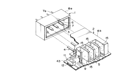
Referring to Figs. 3A through 3C, a high-speed
transmission connector according to a first embodiment of
this invention comprises a male connector 1 and a female
connector 2 which is adapted to connect with the male
connector 1.
The male connector 1 comprises a box-shaped
housing 8a of a resin material having an opening formed
at one end thereof. A plurality of male contact portions
3 are arranged on a bottom of the housing 8a in a matrix
fashion and held to the housing 8a. Each of the male
contact portions 3 comprises a contact pin 7 and a
cylindrical outer conductor 6 as a first outer conductor.
The contact pin 7 has one end provided with a solder
terminal portion 7a outwardly protruding from an outer
wall of the bottom of the housing 8a and has another end
extending within the housing 38a from an inner wall of
the bottom towards the opening. The cylindrical outer
conductor 6 envelopes the contact pin 7 and penetrates
the bottom of the housing 8a.
CA 02211989 1997-07-30
12
The female connector 2 comprises a plurality of
female contact portions 4. Each of the female contact
portions 4 comprises a cylindrical conductive member or
socket member 4a, a cylindrical insulator portion 4b of a
resin material, and a metal plating fllm 16. The
cylindrical conductive member 4a has a clamping leaf
spring portion 13b to contact and hold an outer
peripheral surface of each of the contact pins 7 inserted
upon coupling with the male connector 1. The cylindrical
insulator portion 4b is clamped and held through the
metal plating film 16 by a clamplng leaf spring portion
13a of each of the cylindrical outer conductors 6
inserted simultaneously with the insertion of the contact
pins 7. So that the cylindrical outer conductors 6 are
kept at an earth potential.
The female connector further comprises a housing
8b accommodating and holding the female contact portions
4 arranged on an internal wall of a bottom thereof. The
housing 8b is provided at its rear side with terminals 9.
Each of the terminals 9 extends from each of rear ends of
the cylindrical members 4a, protrudes outwards from each
of holes 10 of the housing 8b, and bends to be inserted
into and connected to each of through holes of a wiring
board 43.
The housing 8b is further provided with insulator
walls or partition walls 5 which are for shielding or
noise-shielding the terminals 9 from one another. Each
of the partition walls 5 has a metal plating film 15
CA 02211989 1997-07-30
formed as a wall metal layer on one surface thereof to
serve as a microstrip line known in the art.
The cylindrical outer conductor 6 shields the
contact pin 7 and the conductive cylindrical member 4a
via the cylindrical protruding portion 4b. Upon coupling
of the connectors, the cyllndrical outer conductor 6 is
brought into contact with a metal plating film 16 formed
as a second outer conductor on the cylindrical protruding
portion 4b. A metal film is found on a projecting
portion 12 of an attaching portion 11. A metal plating
film is formed as a housing metal layer on an outer
surface of the housing 8b and connected to the metal
plating film 15. The metal film on the projection
portion 12 is connected to the metal plating fllm 16
through the metal plating film on the housing 8b. The
attaching portion 11 is fixed to a grounding pad of a
wiring board 43, for example, by the use of a bolt so as
to provide stable grounding. Therefore, the metal
plating films 15 and 16 are electrically connected to the
grounding pad. Thus, a coaxial structure is obtained by
connection of the male contact portions 3 and the female
contact portions 4.
In the above-mentloned connector, the microstrip
lines are formed by the metal plating films 15 on the
surfaces of the partition walls 5 and the terminals 9.
By preliminarily considering and selecting the distance
between each partition wall 5 and each terminal 9, the
dielectric constant of each partition wall 5, and the
CA 02211989 1997-07-30
thickness of the metal plating fllm 15, the microstrip
lines are designed so as to obtain appropriate
characterlstic impedances at the male/female coupling
portion and the terminal portion of the female connector.
Although each terminal 9 extending outwards from
the cylindrical member 4a of the female connector 2 is
perpendicularly bent in the figure, the shape is not
restricted thereto. For example, in order to reduce
conductor resistance of each terminal 9, the terminal may
be slantly bent to reduce its length. The clamping leaf
spring portions 13a and 13b have leaf springs press-
formed to inwardly protrude and are plated at contact
portions by a precious metal such as gold and palladium
so as to improve reliability of connection. For
convenience of illustration, the male and the female
contact portions 3 and 4 of the male and the female
connectors 1 and 2 are specifically defined in the
figure. However, it is obvious that the male and the
female can be reversed.
Referring to Figs. 4A and 4B, the description
will be made as regards a modification of the female
connector illustrated in Figs. 3A through 3C. Similar
parts are designated by like reference numerals. In the
female connector 2 of Figs. 3A through 3C, shielding in
the horizontal direction is provided by the partition
walls 5 while no shielding is provided in the vertical
direction so that noise may possibly enter between those
of the terminals 9 which are ad;acent in the vertical
CA 02211989 1997-07-30
direction.
In the female connector 2 of Figs. 4A and 4B,
each of the partition walls 5 is provided with slits 17.
Metal grounding plates 18a and 18b are inserted through
the slits 17 and assembled. The grounding plates 18a and
18b are provided with elastic locking pieces 20 to be
connected to the metal plating film on the housing 8b
through metal plating layers of the slits 17, and with
solder terminals 19 for connection with a grounding layer
or through holes of the printed board. Like the
foregoing embodiment, the housing 8b is entirely plated
by a metal material except the holes 10 for insertion of
the terminals 9.
By providing the partition walls 5 and the
grounding plates 18a and 18b at the rear side of the
female connector 2, the terminals are completely shielded
from one another. As described above, it is possible to
achieve a design such that appropriate characteristic
impedances are obtained at the male/female coupling
portion and the terminal portion of the female connector.
Referring to Figs. 5A and 5B, the description
will be made as regards another modification of the
female connector illustrated ln Figs. 3A through 3C.
Similar parts are designated by like reference numerals.
In the female connector, the partition walls 5
separating adjacent ones of the terminals 9 have
grounding layers 22 each of which is formed by metal
plating for each individual terminal 9. In the female
CA 02211989 1997-07-30
16
connector of Figs. 3A through 3C, each of the partition
walls 5 is entirely plated to form a common ground so
that ground noise may be produced by simultaneous
driving. In view of the above, the grounding layers 22
are provided for every individual signal terminals and
extend parallel to the terminals 9 along the partition
walls 5, respectively. The grounding layers 22 are
connected to the metal plating films 16, respectively.
Thus, the effect of suppressing the occurrence of noise
is expected. In order to connect the grounding layers 22
of the partition walls 5 to the wiring board, metal-
plated holes (not shown) are provided and solder
terminals 21 are press fitted into the holes in the
manner known in the art.
Referring to Figs. 6A through 6C, the description
will be made as regards a high-speed transmission
connector according to a second embodiment of this
invention. The high-speed transmission connector
comprises a male connector 24 and a female connector 23
adapted to connect with the male connector 24.
The male connector 24 comprises a block-shaped
housing 26 provided with a plate 30 attached to a rear
side thereof. The plate 30 is penetrated by a plurallty
of contact pins 27 arranged in a matrix fashion. The
plate 30 is entirely subjected to metal plating except
those portions of front and rear walls around the contact
pins 27. The housing 26 is provided with introducing
holes 29 for insertion of the contact pins 27. The
CA 02211989 1997-07-30
housing 26 has inner and outer surfaces entirely covered
with a metal plating fllm.
The female connector 23 comprises a cylindrical
contacts 28 each of which comprises an inner terminal 33
as a center conductor and an outer terminal 32
surrounding the inner terminal 33. The inner terminal 33
is conductive and has a clamping portion 34 for
receiving, clamping, and holding a top end of each of the
contact pins 27 upon coupling. The outer terminal 32 is
conductive and has a leaf spring portion 31 arranged
around the inner terminal 33. The leaf spring portion 31
is inserted into each of the introducing holes 29 of the
housing 26 to be brought into contact with the metal
plating film formed on an internal wall of the
introducing hole 29.
The female connector 23 further comprises a box-
shaped housing 25 formed so that the cylindrical contacts
28 are implanted to a rear wall 35. In this event, the
outer terminals 32 and the inner terminals 33 extend from
rear ends of the contacts 28 through the rear wall 35
with protruding outwards from the rear wall 35.
Each of the housings 25 and 26 of the female and
the male connectors and the plate 30 is formed by an
insulating resin material. The housing 26 is entirely
subjected to metal plating. A metal plating film at an
attaching portion 36 of the housing 26 is brought into
contact with an earth pad of a wiring board. The
connector is used as a stacking connector which is for
CA 02211989 1997-07-30
18
connecting parallel substrates.
In the manner similar to the high-speed
transmission connector illustrated in Figs. 3A through
3C, the plate 30 may be provided with partition walls to
separate terminals, i.e. the rear ends of the contact
pins 27 and subjected to metal plating e~cept those
portions holding the terminals. In addition, the
terminals are bent into an L shape. In this event, the
wiring board can be connected in an orthogonal direction,
like the first embodiment. It is noted here that the
male and the female connectors are attached in a reverse
manner.
Turning to Fig. 7, the description will be
directed to a modification of a connector coupling
portion of the high-speed transmission connector of Figs.
6A through 6C. In the connector coupling portion, a male
connector 37 has a housing 39 entirely subjected to metal
plating except those portions into which contact pins 41
are press fitted. Inside the housing 39, protrusions 42
having tapered top ends are formed on a rear wall at
portions where the contact pins 41 are protruded. Around
each protrusion 42, a locking spring portion 44 of a
metal material is implanted. The locking spring portion
44 serves as a first outer conductor.
On the other hand, a female connector 38 has a
housing 40 provided with recessed portions 43 to which
the protrusions 42 of the male connector 37 are guided
and fixed by the locking spring portions 44. An internal
CA 02211989 1997-07-30
19
wall of each recessed portion 43 is also sub~ected to
metal plating and is electrically connected to the metal
plating film of the housing 39 of the male connector 37
upon coupling of the connectors. Each contact 45 has a
clamping portion 46 for clamping and holding each of the
contact pins 41 and an accommodating hole having an
internal wall covered with an insulator layer 47 of an
insulating resin material formed by molding after metal
plating so as to avoid contact with the contact 45 and
short circuit with the metal plating film. Thus, an
outer conductor having a shielding function is substitu-
ted by metal plating except the portions where the
connector pins 41 are implanted and the accommodating
holes of the contacts 45. Therefore, as compared with
the prior art in which the metal component with the outer
conductor press formed is attached, reduction in size and
cost can be achieved.
Referring to Figs. 8A and 8B, the description
will be made as regards a high-speed transmission
connector according to a third embodiment of this
invention. The high-speed transmission connector is
directed to a case where grounding of the connector is
developed to avoid EMI known in the art. Specifically, a
female connector 48 has a housing 51 entirely subjected
to metal plating except the holes 10. A male connector
49 has a housing 50 provlded with a clamplng sprlng
portlon 54 for clamping and holding the exterior of the
housing of the female connector upon coupling of the
CA 02211989 1997-07-30
connectors and with a shielding cylinder or plate 53 to
be electrically connected to the metal plating film 16.
As described in conjunction with Figs. 3A through
3C, partition walls 5 are subjected to metal plating to
form the microstrip lines. Although not shown, a metal
plating film is formed on an attaching portion of the
female connector 48 to be contacted with an earth pad of
a wiring board and kept at an earth potential. The state
upon coupling the connectors is slmilar to that described
in conjunction with Fig. 1 and will not be described any
longer.
As described above, the insulating resin material
is molded and subjected to conductive plating to serve as
the external conductor forming the coaxial connector
having the shielding function. As compared with the
external conductor made of a metal material, each of the
above-mentioned high-speed transmission connectors is
advantageously simple in structure, high in productivity,
and low in cost.
In addition, the thin metal film formed by
plating is used instead of the external conductor formed
by the molded metal article. This allows reduction in
size. Furthermore, the metal films having a matching
impedance are formed on the partition walls separating
the terminals extracted from the connector body. This
achieves impedance matching to obtain desired
transmission characteristics without return loss.