Note: Descriptions are shown in the official language in which they were submitted.
CA 022l23~ l997-08-0~
WO 97/21069 PCT/US96/19448
-- 1 --
GENERATING DATA ABOUT THE SURFACE OF AN OBJECr
Background of the Invention
The invention relates generally to generating representations of a three-
dimensional object on a computer screen, and more parhc~ rly to surface
sensing devices that quickly and efficiently generate data representing the
contour of the surface of a three-dimensional object.
Systems and methods for generating two-dimensional infnrm~tion
about an object are well known. These well known two-dimensional systems
10 typically use a flat table that has a touch sensitive surface. To generate data
for a particular point, a stylus is used to depress the touch-sensitive surface
and cause electrical signals to be generated relating to the position of the
stylus on the table. These stylus position signals may be used to generate
two-dimensional data about the object. These two-dimensional ~1igiti7ing
15 systems, however, are not suitable for generating data about the surface of
three-dimensional objects.
Systems and methods for generating three-dimensional data about an
object and for displaying a representation of the object on a computer screen
are also well known for such applications as computer aided drafting and
20 machining (CAD/CAM), m~ l analysis and visll~li7~tion, and modeling of
objects. These well known three-dimensional data generation devices may
SUB5TITUTE SHEET (RULE 26~
CA 022123~ 1997-08-0~
WO 97/21069 PCT/~JS96/19448
-- 2 --
include either a mechanical probe coordinate measuring machine (CMM), or
an optical system. The CMM systems generally use a type of
electromechanical probe to contact and follow the surface of the object and
generate data relating to the surface of the object along the scan line. The data
generation process is repeated for successive scan lines until data is gathered
for the entire object. Then, the data is combined to form a three-dimensional
representation of the object. The systems for combining scan-line data into a
representation of the object are well known. These mechanical probe systems
are slow because the mechanical probe has to be moved over the entire
surface of the three-dimensional object in order to generate the data. In
lition, these mechanical probe systems require expensive, complex, large
machines, and require a large amount of processing power to control the
mechanical probe and process the scan-line data. In a~l~li*on, only a person
that is specifically trained can ~pelaLe the system.
The known optical systems typically use incandescent light or laser
light to generate data relating to the surface of the object. In one optical
system, light is projected towards the object and the reflected light from the
surface of the object is received by a sensor. In another optical system, a
video camera is used to form images of an object at various different angles to
generate data about the surface of the object. These optical systems can
generate data concurrently for a large portion of the object so that the time
necessary to generate data for the entire object is reduced. These optical
systems, however, are susceptible to misalignment problems that can C~liupl
SUBSTITUTE S~EET (RULE 26)
CA 022123~ 1997-08-0~
WO 97/21069 PCT/US96/19448
-- 3 --
the generated data. In ~ lition, these optical systems are expensive, large
machines that must be operated by a trained person.
All of these known three-dimensional sensing systems are generally
large, expensive, immovable machines. In addition, known types of three-
dimensional sensing systems tend to be complex machines that require a large
amount of data processing. In addition, these known sensing systems are
~lifficll~t for the average person to use because they are so complex, and the
systems can not readily be attached to a personal computer. There is a need
for sensing systems and methods which are relatively simple, inexpensive,
and fast for sensing the surface contour of a ~ree-~ n~ional object to enable
a representation of the object to be generated.
Thus, there is a need for surface sensing systems and methods which
avoid these and other problems of known devices, and it is to these ends that
the present invention is directed.
Summary of the Invention
The invention provides a surface sensing system which is inexpensive,
portable, and can quickly generate three-dimens;onal data about the surface of
an object. The surface sPn~in~ system of the invention may be easily moved
and may also be quickly calibrated. In addition, the surface sensing system is
SUBSTITUTE S~EET (RULE 2~)
CA 022123~ 1997-08-0~
WO 97/21069 PCT/US96/19448
-- 4 --
a device that may be easily int~rf~ e~l to a personal computer and may be
operated by an average person without any specific training.
A surface sensing system in accordance with the invention includes an
array of sensing elements for cont~( ting the surface of the obiect, and a system
associated with each sensing element for providing a signal representing the
location of a corresponding point on the surÇace of the object contacted by the
sensing ~l~m~nt relative to a reference plane. A processor generates a
representation of the object from the signals generated by the sensing
elements. ~ach sensing element may have a system for indicating a relative
displ~c~m~nt of the sensing element with respect to the ierel~nce plane. The
system may use either resistive sensing ~lPn~n~ or reactive, e.g., capacitive,
sensing ~lPmPntc In ~ ition, the array of sensing el~m~nts may be of any
c~ v~nient size and may have a density of sensing elements per unit area that
affords the desired degree of resolution of measurement. The individual
sensing elements may also be of any ~ulLvenient size.
The invention also provides a method for generating a representation of
an object in which the surface of the object is contacted by an array of s~n~ingelements, signals reprPc~onting the locations of points on the surface of the
object relative to fefeLellce plane are generated by the array of sensing
elements, and the signals are processed to generate a representation of the
object.
SUBSTITUTE SI~EET ~R} JLE 26)
CA 022123~ 1997-08-0~
WO 97/~1069 PCT/US96/19448
Brief Description of the Drawings
Figure 1 is a block diagram depicting a surface sensing system in
accordance with the invention;
Figure 2 is a perspective view of an embo~ Pnt of a surface sensing
device in accordance with the invention that may employed with the surface
sensing system shown in Figure l;
Figure 3 is an enlarged cross-sectional view of a first embor~im~nt of a
sensing element of the sensing device of Figure 2;
Figure 4 is a front view of the back mounting plate of the sensing
device shown in Figure 2;
Figure 5 is a front view of the front mounting plate of the sPn~ing
device shown in Figure 2;
Figure 6 is a enlarged cross-sectional view of another embodiment of a
sensing element of the sensing device of Figure 2;
Figure 7 is a side view showing the surface sensing device of the
invention being used to generate data about a three-dimensional object;
Figure 8 is a top view showing the surface scanning device of the
invention being used to generate data about the three-~imPn~ion~l object of
Figure 7;
Figure 9 is a flowchart showing a method of sensing a three-
dimensional object in accordance with the invention; and
Figure 10 is a flowchart showing a method of sensing one side of a
three-dimensional object in accordance with the invention.
SlJ8STITUTE SHEET (R~L~ 26)
CA 022123~ 1997-08-0~
WO 97/21069 PCT/US96/1~448
-- 6 --
Detailed Description of Ple~ll~d ~mbodiments
The invention is particularly applicable to a surface sensing system and
method that provides an inexpensive, fast way of sensing a three-dimensional
object, such as small hand-held objects, to produce data about the surface of
the object, to permit generation of a representation of the object on a computerscreen, and will be described in that collL~,cl. It will be appreciated, however,
that the system and method in accordance with the invention has ~,~ealel-
utility.
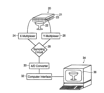
Figure 1 is a block diagram depicting a sensing system in accordance
with the invention. The sensing system may include a surface sensing device
20 that will be described in more detail below with reference to Figures 2-6.
The surface sensing device 20 is generally used to generate data about the
surface characteristics of a three-dimensional object 22. Generally, the surfacesensing device generates signals that represent the contour of the surface of
the object. This may be by signals that represent the locations, e.g., heights, of
various points on the surface of the object relative to a reference plane. Once
these signals are produced, they can be processed to generate representAhnn~
of the object that may be displayed on a computer screen. The data or the
representations may also provide data to a computer aided design (CAD)
package or any other system that can manipulate object data. The surface
sensing device may have a plurality of sensing elements 23 arranged in an
array or matrix supported by a mounting plate 21. However, the surface
CA 022123~ 1997-08-0~
WO 97~21069 PCT/US96/19448
-- 7 --
sensing device may be composed of any number of sensing elements in any
desired configurations and may have any desired density of sensing elements
per unit area. The matrix of sensing elements may be an X-Y matrix of
sensing elements. These sensing elements will be described in more detail
below.
In this embodiment, an X multiplexer 24 and a Y multiplexer 26 may be
used to sequentially sample each sensing ~l~mpnt within the X-Y matrix in
order to de~lmil,e the signals from each individual sensing element in the
array. Thus, the X multiplexer and the Y multiplexer allow the sensing
system to scan each row and column of the array of sensing ~lPm~ntc in order
to generate signals for each individual point on the surface of the object
contacted by the corresponding sensing element. The matrix of sensing
elements may also be sampled by any other sampling system, such as multiple
parallel inputs. The method of generating three-dimensional data using these
multiplexers will be described in more detail below.
Each sensing element has a system associated with it for producing a
signal repr~c~nfing the location of a point on the surface of the object
contacted by the sensing element relative to a reference plane. ~n other words,
each sensing element has a system that cullv~iL~ the signal from the sensing
element into a signal that corresponds to the location of a point on the surfaceof the object relative to a ler~,~nce plane. Once the signals representing the
location of a point on the surface of the obiect relative to a refei~nce plane are
SU~TIT~TE SH~T ~RULE 26)
CA 022l23~ l997-08-0~
WO 97/21069 PCT/US96/19448
-- 8 --
produced, the signal are then processed to generate a representation of the
object. No complex calculations or systems for controlling the sensing device
are required. Thus, data about the surface of the object may be generated
quickly and inexpensively. The system for producing the signals representing
the location of points of the surface of the object relative to a rer~l~nce plane
and the processing system will be described in more detail below.
The system for producing the signals representing the location of points
of the surface of the object relative to a refelel,ce plane may include a
sampling circuit 28. This sampling circuit may be a high frequency A/C
cap~ it~n~ e bridge that generates an ~le~ tri~ ~l signal correspontling to the
capacitance of a capacitive sensing ~lPm~nt, or a Wh~t~t ne bridge that
generates an Plectri~ ~l signal corresponding to the resistance of a resistive
sensing element. The capacitive sensing element will be described below with
rerel~-,ce to Figure 3, and the resistive sensing element will be described
below with Lefefellce to Figure 6. The A/C capacitance bridge and the
Wheatstone bridge ~mpl~ either the capacitance or r~si~hn- ~, respectively, of
the sensing element and generate a corresponding ~l~rtri~ Al signal. Once all
of the electrical signals are generated by the sampling circuit, the signals areconverted into digital signals by an analog-to-digital (A/D) c~l,vellel 30.
After these signals are col-verLed into a digital format, they are fed into a
computer interface 32. The computer int~rf~ce may be a microprocessor. The
computer interface 32 controls the operation of the X multiplexer 24 and the Y
multiplexer 26 in order to generate signals for each sensing element of the
SUBSTITUT~ S~ I~ET (RULE 26)
CA 022123~ 1997-08-0~
W O 97/21069 PCTAUS96/19448
_ g _
sensing device and also processes the signals from the signal producing
system in order to generate a representation of the object that can be
displayed on a computer display. The computer interface, in turn, may be
connected to a computer 34 that has a display 36.
Figure 2 is a perspective view of the sensing device 20 shown in Figure
1. As shown, the sensing device may comprise a plurality of individual
sensing elements arranged in an array or matrix. The sensing device may
include a front mounting plate 50 and a back mounting plate 52. In A~ ion,
there are a plurality of sensing elements 23 that are connected between the
front mounting plate and the back mounting plate. These sensing ~l~mQnt~
may be any type of sensing device that provides a signal representing the
location of a point on the surface of an object relative to a refel~nce plane.
eL~l,ed embodiments of these sensing elements will be described in more
detail below with rere~ ce to Figures 3 and 6.
Each of the sensing ~l~m~nt~ may comprise a body portion 54 having a
sensing pin 56 that is biased to extend outwardly from the end of the sensing
element body. For clarity, only a small number of sensing elements and
sensing pins are shown in Figure 2, but the sensing device may have, for
example, a full X-Y matrix of sensing ~l~m~nt~ of any a~lot,liate size and
density. The sensing pins may be of any desirable length and depends on the
size of the object. The plurality of the sensing elements may form an array of
sensing elements. The number of sensing elements within the array per unit
SlJ~STITll~ SHE~T (RULE 26)
CA 022123~ 1997-08-0~
W O 97/21069 PCT~US96/19448
- 10 -
area and the spacing of the sensing ~l~m~nt.~ within the array, e.g., the density
of sensing elements, determine the resolution of the sensing device. For
example, if the array has many closely spaced sensing elements, then the
sensing device has a high resolution. On the other hand, an array with fewer
sensing elements spaced farther apart from each other has a lower resolution.
The number and spacing of the sensing elements in the array may vary and
be selected for the resolution required for a particular application. In fact, the
sensing ~l~m~nt~ within the array may be detachable from the front and back
mounting plates, if desired, so that the array may be custnmi7e~1 easily. ~ach
sensing element independently generates a signal representing the location of
a point on the surface of the object relative to a reference plane. In other
words, the sensing elements det~rmine a contour of the surface of an object by
measuring the location of a point on the surface of the object relative to any
plane. The rereLence plane may be the back mounting plate so that the
sensing elements measure the height of points on the surface of the object
relative to the back mounting plate. If the Le~Lence plane is the back
mounting plate, then the sensing device of ~e invention may be used to
produce data about an object even if the sensing device is upside down.
However, the l-efe:Lence plane may be any other plane, such as the surface
upon which the object is resting.
Figure 3 is a cross-sectional side view of a first embodiment of a
sensing element 23 that may be employed in the sensing device 20 shown in
Figure 2. The sensing element shown in Figure 3 is a capacitive sensing
SUBSTITUTE SHEET ~UL~ 26)
CA 022l23~ l997-08-0~
WO 97/21069 PCT/US96/19448
- 11 -
element 55 that may be attached between the front mounting plate 50 and the
back mounting plate 52 of the sensing device. The capacitive sensing element
is a variable capacitance device, and may include a sensing pin 56 that is
slideably disposed within a cylindrical housing 72, and biased outwardly from
the housing by a spring 66. An interior end of the sensing pin may be
attached to a stopper and sliding guide 64. The spring 66 may engage the
guide 64 to bias the sensing pin outwardly through the front mounting plate.
In addition, an insulating pin guide 68 disposed in front plate 50 may guide
the sensing pin, and a back plug 70 may attach the spring to the back
mounting plate.
The sensing pin 56 and the cylin~lric~l housing 72 that surrounds the
sensing pin may both be m~t~llir The combination of the metallic sensing pin
56 and the cylindrical housing 72 form a capacitor whose capacitance varies
with the location of the sf~n~;n~ pin in the cylindrical housing. In other
words, the distance that the sensing pin is pushed back into the cylindrical
housing may be determined by measuring the change in capacitance relative
to a re~fence value. The capacitive sensing element may also include an
outer shielded housing 74 that protects the capacitor from damage. An
electrical brush contact 76 connects the sensing pin 56 to the front mounting
plate 50. The cylindrical housing 72, which is the other part of the capacitor,
is connected to the back mounting plate 52 by the back plug 70. Thus, the
capacitance of the capacitive sensing element is measured by measuring the
capacitance of the electrical circuit formed by the electrical brush contact, the
sensing pin, the cylindrical housing, and the back plug.
SlJBSTITlJ~ SH~T (RU~ 26)
CA 022123~ 1997-08-0~
WO 97/21069 PCT/US96/19448
- 12 -
Figure 4 is a front view of the back mounting plate 52 of the sensing
device shown in Figure 2. As shown, the back mounting plate may have a
plurality of ~lectTi( ~l traces 8Q that vertically (in this figure) connect the back
plug 70 and the cylindrical metallic housing (not shown) of various sensing
elements of the sensing device to each other. One end of all of the .olPctrir~
traces 8û are connected together to form a c mmcn lead 82. The other ends of
the ~lectri~l traces are combined into a cable 84 as individual conductors that
connect to the Y multiplexer (not shown).
Figure 5 is a front view of the front mounting plate 50 of the sensing
device as shown in Figure 2. The front mounting plate may also have a
plurality of ~lertric~l traces 90 that are connected to a hnri~orl~l (in this
figure) row of electrical brush contacts 76 of various sensing elements. One
end of these electrical traces are connected together to form a second commnn
lead 92. The other end of the electrical traces are combined in a cable 94 as
individual conductors that connect to the X multiplexer (not shown).
In operation, when the sensing device with a plurality of capacitive
sensing elements is placed over an object to be sensed and the device is
pushed down, each sensing pin is displaced into the cylindrical housing a
certain amount depending on the height of tl~e cc,lles~onding point on the
2û surface of the obJect which the pin contacts, and the spring is c~ essed.
When each sensing pin is pushed back, more of the sensing pin is in close
proximity to the cylindrical housing and the capacitance of the sensing
S~iBST~UTE SHEET (RULE 26)
CA 022l23~ l997-08-0~
W O 97/21069 PCTrUS96/19448
- 13 -
element increases. The electrical traces 80, 90 form an X-Y matrix of
conductors. The cap~-it~n~e of each individual sensing element may be
measured by selecting a particular ~lectrit-~l trace on the back mounting plate
using the Y multiplexer, and a particular electrical trace on the front mountingplate using the X multiplexer which intersect at the selected sensing .olf~mPnt
For example, with LeferelLce to Figures 3, 4 and 5, to measure the capacitance
of a selected sensing element 9~, an electrical trace 97 on the back mounting
plate in combination with an electrical trace 98 on the front mounting plate ares~lerte~1 by the multiplexers. The capacitance is then measured by the
sampling circuit as the capacitance of the electrical circuit formed by the
electrical trace 97, the back plug 70, the cylindrical housing 72, the sensing pin
56, the ~ ctrir~l brush contact 76, and the electrical trace 98.
Figure 6 is a cross-sectiona~ view of another embo~limPnt of a sensing
element 23 that may be employed in the ~n~ing device 20 shown in Figure 2.
The sensing element shown in Figure 6 is a resistive sensing element 100 that
may have a sensing pin 102 slideably disposed within a guide housing 104
that may have a resistive strip 106 attached to it. The sensing pin is biased
outwardly from the housing by a spring 109. The resistive sensing ~l.om~nt is
a variable resistance device. The sensing pin and guide housing may both be
metallic. An interior end of the sensing pin may be attached to a stop plug
108, and the sensing pin is guided through the front mounting plate 50 by a
front guide 110. A front electrical brush contact 112 electrically connects the
sensing pin to an electrical trace ~not shown) of the front mounting plate 50.
SUBSTITUTE SHEET (RULE 26)
CA 022123~ 1997-08-0~
WO 97/210G9 PCT/US96/19448
- 14 -
A rear stopper 114 connects the guide housing 104 to the baclc mounting plate
52. A second electrical brush contact 116 electrically connects the sensing pin
to the resistive strip. An electrical connector 118 connects the resistive strip to
the electrical traces (not shown) on the back mounting plate 52. The electrical
traces of the front and back mounting plates, described above with rererel.ce
to Figures 4 and 5, may also be used in connection with this resistive sensing element.
In operation, as each resistive sensing pin is displaced into the guide
housing a certain amount depending on the height of the corresponding point
on the surface of the object which the sensing pin contacts, the second
electrical brush contact 116 slides backwards over the resistive strip 106 and
the resistance of the resistive sensing PlPmPnt is reduced. The resistance of anindividual resistive sensing element is deLe~ ed by selecting the individual
resistive sensing element using the multiplexers and by using the sampling
circuit to measure the resistance OIC the electrical circuit formed by the
electrical trace on the front mounting plate, the front electrical brush contact112, the sensing pin 102, the second electrical brush contact 116, the resistivestrip 106, the electrical connector 118, and the Ple~ l trace on the back
mounting plate. Thus, the resistive sensing element has a varying resistance
that can be measured by the sampling circuit, such as a Wheatstone bridge, as
described above, and co~ ell~d into an electrical signal representing the
height of a particular point on the surface of the object above a lefelence
plane.
SUBSTI~UTE ~iH~ET (P~l~LE ~)
CA 022123~ 1997-08-0~
WO 97/21069 PCT/US96/19448
- 15 -
Figure 7 is a side view of the surface sensing device of the invention
being used to generate data about a three-dimensional object 13~, such as a
vase. The object 130 is three-dimensional, but only its side shape is shown for
darity. In order to generate data representing the entire object 130, data must
be generated for two or more sides of the object by moving either the object or
the sensing device. The surface sensing device 20 may be placed over the
vase so that the front mounting plate 50 is near the highest surface of the vase.
In locations where the surface of the vase has some height, the sensing pins 56
of the sensing elements 54 are pushed back various distances depending on
the height of the surface of the vase. The varying distances of the sensing
pins cc.lre*)ond to varying capacitance or resistive values of the sensing
element, as described above. At locations where the surface of the vase is not
present, the sensing pins 56 are fully extended due to the spring and have a
maximum resistance value or a minimum capacitance value, depending on the
type of sensing element used. The length of the sensing pins may plererably
be long enough so that the sensing pins, that do not touch the surface of the
object, contact the surface that the object is resting on.
Figure 8 is a top view of the sensing device 20 of the invention being
used to generate data about the object 130. The array of sensing elements 56,
in this embodiment is a rectangular configuration, but any configuration, such
as a circle or square may be used. The number of sensing elements within
the array of sensing elements may be increased or decreased depending on the
size of the object and the desired resolution. As described above, the array of
Sl~SSTITUTE SHEET (RUEE 26~
CA 022123~ 1997-08-0~
WO 97/21069 PCT/US96/19448
- 16 -
sensing ~l~m~nt.~ allows the sensing device to generate data for a large portionof an object quickly. If the object is larger that the sensing device, then extra
sensing elements may be added. If the object is still too large with the
addition of the extra sensing elements, then data about the surface of the
entire object may be generated by repeatedly using the sensing device of the
invention and then proc~c~ing the data to produce a representation of the
object.
Figure 9 is a flowchart showing a method of sensing a three-
dimensional object and generating a repr~PntAtion of the object in accordance
1~ with the invention. The method is started in Step 140. In Step 142, the
heights of various points on a first side of an object are det~rmin~o~l using the
sensing device. Then in Step 144, the data for another side of the object is
generated using the sensing device. In Step 146, it is deLe~ ined whether or
not data has been generated for all of the sides of the object. For example, thevase shown in Figures 7 and 8 may require two sides of the vase to be sensed
using the scanning device in order to generate sufficient data. The details of
sensing each side of an object are described below with Le~e~ence to Figure 10.
~f ~ 1itional sides of the object need to be sensed to generate sufficient data,then the method returns to Step 144, and data for another side of the object is
generated. As the surface of a three-~ n.~ional object becomes more
complex, data for additional sides of the object may be required. On the other
hand, if all sides of the object have been sensed and sufficient data has been
generated, then in Step 148, the data from the various sides of the object are
SIJBSTITUTE SHEET (RULE 26~
CA 022123~ 1997-08-0~
WO 97/21069 PCT/US96/19448
- 17-
processed and combined together to generate a representation of the object.
The technique for combining the data for the various sides of the object to
generate the representation of the object is well known. The method is then
completed in Step 150. In this manner, a graphical representation of a three-
dimensional object may be generated and displayed on a co~ ulel system.
Pigure 10 is a flowchart showing a method of generating data for each
side of a three-dimensional object in accordance with the invention. In Step
160, the method is begun. In Step 162, a first electrical trace on the front
mounting plate is SPlP~ tP~ by the X multiplexer. This first electrical trace
horiYor~t~lly connects a number of sensing PlPmPnt~. In Step 164, a first
Plectri~ ~l trace on the back mounting plate is ~PlPctP-l by the Y multiplexer.
The combination of the Plectric~l trace of the front mounting plate and the
Plectri~-~l trace of the back mounting plate selects a single sensing element that
is then sampled in accordance with the invention. In Step 166, the next
sensing element in the row sPlectP~1 by the X multiplexer is sampled by
incrPmpnting the Y multiplexer. In Step 168, it is detPrminPtl whether or not
the row is complete (i.e., whether each sensing element in the row has been
sampled). If the row has been completed, then the method returns to Step 166
in which the next column is selected by the Y multiplexer and the next
sensing element is the row is sampled. If the row is complete, it is then
detPrminPA in Step 170 whether or not the entire scan of the array has been
completed. If the scan has not been completed, then the method returns to
Step 162 in which the next row of sensing Pl~mPnt~ is selected by selecting the
BSTITUTE SHEET (RULE 26)
CA 02212355 1997-08-0~
WO 97/21069 PCTtUS96119448
- 18 -
next Plectri~l trace on the front mounting plate. On the other hand, if the
scan is done then the method is completed in Step 172. In this manner, using
the X and Y multiplexers, the entire array of sensing elements are scanned and
signals are generated for each element. These signals are then processed and
turned into Plectri~l signals representing the height of the surface of the
object above a refelellce plane.
The three-dimensional sensing device of the invention may also be
~uickly and easily calibrated by placing an object with a known surface
contour, e.g., flat, un~l~rn~th the sensing device. Then, the actual output of
the sensing device may be compared to the anticipated output and the sensing
device may be adjusted. This process of calibrating the sensing device may be
conducted by the computer int~rhce
While the foregoing has been with le~e~ellce to a particular embodiment
of the invention, it will be appreciated by those skilled in the art that changes
in this emboflinl~nt may be made without departing from the principles and
spirit of the invention, the scope of which is defined by the appended claims.
SUBST~TUTE SHEET (P~ULE 26)