Note: Descriptions are shown in the official language in which they were submitted.
CA 02212504 2004-07-16
BACKGROUND OF THE INVENTION
1. Field of the Invention
The present invention relates to power factor
correction, harmonic filtering and load balancing of
currents drawn from an AC utility power line by a load.
2. Description of the Prior Art
Loads connected to AC utility power lines
ideally draw current that is directly in phase with the AC
voltage source, is drawn equally on all phases from a
polyphase source, and is of the same frequency as the line
voltage. Current drawn in this fashion minimizes demand on
the power source and on the distribution lines and induces
no distortion of the source voltage. Many loads, however,
such as motors, motor drives, computers, fluorescent
lighting, and the like, do not draw power from the utility
power lines in this manner.
Various prior art arrangements have been
developed to correct the above-mentioned problems. For
example, loads having an inductive displacement power
factor can be corrected by installing power factor
correction capacitors in parallel with the equipment. If
sized correctly, such capacitors will supply reactive
current that is directly in phase with the reactive current
drawn by the load. Hence, reactive currents will circulate
between the capacitors and the load thus requiring no
reactive power to be supplied by the source. While
effective, capacitors can only be utilized effectively if
the load is constant at all times. If the load varies,
however, different amounts of capacitance must be connected
to the line to avoid having reactive power being drawn from
the source when no current is actually needed by the load.
Another problem with power factor correction capacitors is
the introduction of unwanted resonance in the power lines.
Switching systems, such as switching power supplies, which
abruptly change their capacitance, are especially
susceptible to such resonance in the power lines. Moreover,
CA 02212504 2004-07-16
if a power factor correction capacitor is successfully
installed, a different load connected to the line may
degrade the performance of the system. Moreover, power
factor correction capacitors do very little to correct the
problems of harmonic currents and unbalanced loads.
Harmonic currents drawn by many non-linear loads
that rectify the AC voltage to produce a DC supply or that
phase control the AC voltage may adversely affect the power
transmission system. The added current that the power
transmission system must supply results in higher
transmission losses that can cause large heat losses in
transformers of the transmission system. Such losses
require over-sized transformers. Moreover, harmonic
currents can often distort the AC voltage source which can
cause other equipment on the power lines to fail or perform
poorly. A trap filter can be utilized to filter such
harmonics. However, a separate trap filter is needed for
each harmonic. A problem with trap filters, however, is the
resonance caused thereby, just as in the case of the power
factor correction capacitors. Still another problem is that
trap filters will also try to shunt harmonics from loads
other than the load to which it is attached. Hence, the
trap filter's capacity is exceeded, with corresponding
failure of the trap filter.
It is, therefore, an object of the present
invention to provide an active harmonic filter which
overcomes these problems of the prior art devices. It is an
object of an aspect of the present invention to provide an
active harmonic filter that sources~current to or draws
current from the supply line at appropriate times to reduce
or eliminate load induced phase shifts between the line
voltage and the line current. It is a further object of an
aspect of the present invention to provide an active
harmonic filter that reduces or eliminates line harmonics.
It is yet another object of an aspect of the present
invention to provide an active harmonic filter that
2
CA 02212504 2004-07-16
balances the currents drawn on all phases of a polyphase AC
source. Still other objects of aspects of the present
invention will become apparent to those of ordinary skill
in the art upon reading and understanding the following
detailed description of the preferred embodiments.
SUMMARY OF THE INVENTION
Accordingly, the present invention provides in
one aspect an active harmonic filter connectable to a power
line that provides electric energy from a source to a load.
The active harmonic filter includes a controller and an
electric energy storage device which stores electric
energy. An invertor is connected between the electric
energy storage device and the power line. The invertor
controls current flow between the electric energy storage
device and the power line in response to a firing command
from the controller. A line current detector is positioned
to detect current flowing in the power line and to provide
an indication of the detected line current to the
controller. A filter current detector is positioned to
detect filter current flowing between the electric energy
storage device and the power line and to provide an
indication of the detected filter current to the
controller. The line current and the filter current are
combined to form a load current supplied to the load. A
conductor is connected to the power line for enabling the
controller to detect the voltage on the power line. The
controller includes one or more of (i) a predictor which
predicts in advance from samples of line current, filter
current, and line voltage a first adjustment to be combined
with the firing command to cause the invertor to at least
one of supply filter current to and draw filter current
from the power line; (ii) an integrating slow control which
integrates differences between actual line current and
desired line current in equivalent times in difficult
cycles of the line voltage and which generates therefrom a
second adjustment that is combinable with the firing
3
CA 02212504 2004-07-16
command; (iii) a proportional controller which generates
from differences between actual line current and desired
line current a third adjustment that is combinable with the
firing command; and (iv) a current balancer which balances
currents in two or more lines of the power line as a
function of samples of the line current and line voltage.
According to another aspect of the present
invention there is provided a method of reducing on an AC
power line at least one of phase shift between line voltage
and load current, and a harmonic of the load current. The
method includes sampling load current and the line voltage
at a plurality of sample times during a first cycle of the
power line. For each sample of load current and line
voltage, a desired load current that is in phase with the
line voltage is determined. For each of the plurality of
sample times, a first difference current between the
desired load current and the sampled load current is
determined. From closely adjacent pairs of first difference
currents, a plurality of second difference currents are
determined. Each second difference current corresponds to
the difference between one closely adjacent pair of first
difference currents. Each second difference current is
combined with the actual line current at a time during a
second cycle of the power line having a select temporal
relation to each pair of first difference currents in the
first cycle of the power line corresponding to each said
second difference current.
The method may also include the steps of sampling
load current and line voltage at a plurality of sample
times during the second cycle of the power line equivalent
to the plurality of sample times during the first cycle of
the power line. At a sample time during the second cycle of
the power line, a stored second difference current is
retrieved. The retrieved second difference current is
determined at a time intermediate the sample time during
the second cycle of the power line and equivalent sample
4
CA 02212504 2004-07-16
time during the first cycle of the power line. The
retrieved second difference current is combined with the
load current at a time during the second cycle of the power
line equivalent to the intermediate sample time.
According to yet another aspect of the present
invention there is provided an active harmonic filter
connectable to a power line that provides electric energy
from a source to a load. The active harmonic filter
comprises a controller connected to detect line voltage and
to line current of the power line and to provide a firing
signal that varies in response to changes in the line
voltage. An invertor is connected between the power line
and a source of stored energy and connected to receive the
firing signal from the controller. A first determiner
determines from the line voltage and line current a desired
line current that will provide to the load the necessary
electrical power required for operation thereof and is in-
phase with the line voltage. A second determiner
determines differences between the line current and the
desired line current. A predictor determines from two or
more closely adjacent differences between the line current
and desired line current during a first power line cycle a
first adjustment combinable with the firing signal to cause
the invertor to produce a filter current that when combined
with the line current reduces one of load induced phase
difference between the line voltage and the line current,
and a line current harmonic.
According to still yet another aspect of the
present invention there is provided a method of reducing on
an AC power line a harmonic of the line current. The
method comprises sampling line current and line voltage at
a plurality of equivalent sample times during a first and
second cycle of the power line. For each sample of line
current and line voltage, a desired line current that is
determined is in-phase with the line voltage. For each of
the plurality of sample times, a difference current between
5
CA 02212504 2004-07-16
the desired line current and the sampled line current is
determined. At least one of (i) integrating the difference
currents in equivalent times of the first and second cycles
of the power line, generating from each integration a
corresponding integrated difference current and combining
each integrated difference current with the line current;
and (ii) proportionally controlling each of the plurality of
difference currents, generating from each of the plurality
of proportionally controlled difference currents a
corresponding proportionally controlled difference current
and combining each proportionally controlled difference
current with the line current is performed.
According to still yet another aspect of the
present invention there is provided a method of balancing
line currents of a polyphase AC source. The method
comprises determining phase-to-neutral power provided to
the load by each phase. An average power provided to the
load by each phase is determined. An average RMS line
current provided to the load by each phase is determined
from the arrange point. The RMS line currents that are one
of sourced to and drawn current from the phases as a
function of the average RMS line current provided to the
load by each phase are balanced.
According to still yet another aspect of the
present invention there is provided an active harmonic
filter connectable to two lines of a single phase AC power
line. The filter comprises a controller connected to
measure the line voltages and the line current. An invertor
including three poles, two of the poles utilized to switch
power between the invertor and the power lines and the
third pole utilized to switch power from the invertor to a
third power line, wherein the controller controls the
firing of the three phases to selectively one of source
current to and draw current from the three power lines.
5a
CA 02212504 2004-07-16
BRIEF DESCRIPTION OF THE DRAWINGS
Embodiments of the present invention will now be
described more fully with reference to the accompanying
drawings in which:
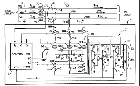
Fig. 1 shows a circuit diagram of an active
harmonic filter in accordance with one embodiment of the
present invention connected to a 3-phase power line;
Fig. 2 shows a block diagram of the internal
components of the controller C of the active harmonic
filter of Fig. 1;
Fig. 3 shows a voltage waveform of the voltages
appearing on the 3-phase power lines of Fig. 1. referenced
to a neutral;
Figs. 4a-4b show current and voltage waveforms of
a portion of the voltage waveform in Fig. 3 including
current and voltage waveforms produced by the filter F in
Fig. 1;
Figs. 5a-5d show a software flow diagram of a
control routine implemented by the controller C in Fig. 1;
Figs. 6a-6c show voltage waveforms of the duty
cycles of transistors of the filter F of Fig. 1;
Fig. 7 shows an exemplary line-to-neutral voltage
and line current with a desired load current and filter
current superimposed thereon;
Fig. 8 shows an exemplary desired line current
and an exemplary actual line current; and
Fig. 9 shows a circuit diagram of an active
harmonic filter in accordance with another embodiment of
the invention connected to a 3-phase power line P that
includes a neutral.
5b
CA 02212504 1997-10-31
DESCRIPTION OF THE PREFERRED EMBODIMENTS
With reference to Fig. 1, an active harmonic
filter F is connected to a power line P utilized to
convey AC power from a 3-phase source to a load. The
power line P includes three lines 2, 4 and 6 that are
utilized to convey the voltages V~, VBC and VcA and the
line currents Ice, ILB, and ILC of phases A, B and C,
respectively, of the source to the load. The source of
AC power may be Delta or Y connected. If Y connected, a
neutral (shown in Fig. 9) may also be provided between
the source and the load.
The active harmonic filter F includes a
controller C that controls an invertor I to selectively
source current to or draw current from the lines 2, 4 and
6 to reduce load induced phase differences,between the
voltages V~, VBC and VcA and the currents Ice, ILB, and
ILC, respectively, reduce line current harmonics and
balance the currents in lines 2, 4 and 6.
The invertor I includes a plurality of
transistors 10-20, such as IGBTs, that are utilized to
selectively source current to or draw current from the
lines 2, 4 and 6. The emitter terminals of transistors
10, 12 and 14 are connected to the collector terminals of
transistors 16, 18 and 20 and form nodes 24, 26 and 28,
respectively. A pair of series connected capacitors 32-
34 are connected in parallel with the series connected
transistors 10-16, 12-18 and 14-20. Connected between
the emitter terminal and the collector terminal of each
transistor 10-20 is a diode 36. Each diode 36 has its
anode connected to the emitter terminal and its cathode
connected to the collector terminal of corresponding
transistors 10-20.
Connected between nodes 24, 26 and 28 and the
lines 2, 4 and 6 are power inductors 40, 42 and 44 and
high frequency block inductors 46, 48 and 50,
respectively. The junction of the high frequency block
inductors 46, 48 and 50 and lines 2, 4 and 6 form nodes
- 6 -
CA 02212504 1997-10-31
54, 56 and 58, respectively. Connected between lines 2-
4, 4-6 and 6-2 are high frequency traps/bypasses 60.
Each high frequency trap/bypass 60 includes an inductor
62 and a capacitor 64 connected in series and having a
resonant frequency, preferably, at or near a switching
frequency of the invertor I. A capacitor 66 is
connected in parallel with the series connected inductor
62 and capacitor 64. The capacitor 66 is utilized to
pass between lines 2, 4 and 6 frequencies above the
resonant frequency of the series connected inductor 62
and capacitor 64.
Line current sensors 70, 72 and 74 are
positioned to detect the line currents Ice, ILB and ILK in
lines 2, 4 and 6, respectively, and to provide outputs
corresponding thereto to the controller C. Preferably,
the line current sensors 70, 72 and 74 are Hall effects
or current transformers. Filter current sensors 80, 82
and 84 are positioned to detect the filter currents IFA~
IFB and IFC flowing in the power inductors 40, 42 and 44,
respectively, and to provide outputs corresponding
thereto to the controller C. Preferably, the filter
current sensors 80, 82 and 84 are Hall-effect type
sensors.
Conductors 86, 88 and 90 are connected between
the controller C and lines 2, 4 and 6, respectively, to
enable the controller C to selectively detect the
voltages VAB, and VB~ across lines 2-4 and 4-6.
Conductors 92 and 94 are connected across the capacitors
32-34 and to the controller C to enable a voltage VDC
impressed on the capacitors 32-34 to be detected by the
controller C. The transistors 10-20 have base terminals
that are connected to the controller C which supplies
pulse-width-modulated (PWM) signals thereto.
The controller C includes a pre-charge PC
output that is connected to a gate terminal of an SCR 96
or other suitable half-phase switching device. Connected
in series with the SCR 96 is a resistor 98. The SCR 96
_ 7 _
CA 02212504 1997-10-31
has its anode terminal connected to one of the lines,
e.g., line 2. The side of the resistor 98 opposite SCR
96 is connected to the side of power inductor 40 opposite
node 24. The controller C has a line contactor output LC
that is utilized to control the operation of a line
contactor 100 that controllably isolates the inductors 40
and 44 from lines 2 and 6, respectively, during pre-
charging of the capacitors 32-34. A breaker BR is
utilized to connect the inductors 46, 48 and 50 to the
lines 2, 4 and 6.
To pre-charge the capacitors 32-34, the line
contactor 100 is opened and breaker BR is closed. The
controller provides firing signals on its PC output that
cause the SCR 96 to turn-on for progressively longer
half-phase intervals. For each on-time of the SCR 96,
line 2 is connected to the side of inductor 40 opposite
node 24 thereby enabling current to flow from line 2
through SCR 96 and resistor 98 and through inductor 40 to
node 24. From node 24, the current flows through diode
36 of transistor 10, through capacitors 32-34 and through
diode 36 of transistor 18 to node 26. From node 26 the
current flows through inductors 42 and 48 to line 4. The
inductors 40 and 42 and resistor 98 avoid excessive in-
rush current when the capacitors 32-34 are first
connected between lines 2 and 4. When the capacitors 32-
34 are charged to a sufficient level, the controller C
terminates the firing signals and outputs on the line
contactor output LC a signal that causes line contactor
100 to close and connect inductors 40 and 44 to lines 2
and 6, respectively. The controller C provides modulated
PWM signals that enable transistors 10-20 and power
inductors 40, 42 and 44 to co-act and charge capacitors
32-34 to a voltage VDC, preferably, about 15% above the
peak voltage appearing across lines 2-4, 4-6 and 6-2.
For example, for a 480 VAC voltage measured across lines
2-4, the capacitors 32-34 are charged to approximately
780 volts.
- g _
CA 02212504 1997-10-31
With reference to Fig. 2 and with continuing
reference to Fig. 1, the controller C includes a voltage
signal conditioner 104 which is connected to lines 2, 4
and 6 via the conductors 86, 88 and 90. The voltage
signal conditioner 104 conditions and provides to an A/D
converter 106 voltages V~ and VBC and provides to a
microcontroller 108 phases 6~ and OB~. The
microcontroller 108 includes support circuitry (not
shown), such as a memory unit that includes RAM and ROM,
I/O drivers, timers and the like. The voltages VAB and
VB~ are converted by the A/D converter 106 to
corresponding digital values which are provided to the
microcontroller 108. The microcontroller 108 provides
synchronization and control signals to the A/D converter
106 to control the operation thereof. A current signal
conditioner 110 receives the output of line current
sensors 70, 72 and 74 and filter current sensors 80, 82
and 84. The signal conditioner 110 conditions the
received signals and provides conditioned signals
indicative of the line currents Ice, ILB and ILK and the
filter currents IFA, IFB and IFS to the A/D convertor 106
which converts the conditioned signals into digital
values which are provided to the microcontroller 108.
An AC/DC power supply 112 is connected across
two of the lines, e.g., 2-4 and, converts AC power
therefrom into DC control voltages utilized by internal
circuitry of the controller C. The power supply 112 also
provides a reference voltage signal ILEVEL to an inverting
input of a comparator 114 that has its non-inverting
input connected to detect a conditioned signal
corresponding to the output of one of the filter currents
sensors 80, 82 and 84. The output of the comparator 114
is provided to a current trip latch 116. When a current
detected by one or more of filter current sensor 80, 82
and 84 produces a voltage that exceeds the reference
voltage signal ILEVEL~ the output of the comparator 114
changes in state. In response to this change in state,
- 9 -
CA 02212504 1997-10-31
the current trip latch 116 provides a signal to the
microcontroller 108 and driver 120 which causes the PWM
signals provided to the transistors 10-20 to be
terminated. The termination of PWM signals to the
transistors 10-20 causes the filter F to terminate
sourcing current to or drawing current from lines 2, 4
and 6.
A line driver 120 is connected to receive from
the microcontroller 108 data corresponding to desired
duty cycle of the PWM signals provided to the transistors
10-20. The driver 120 converts the supplied data into
the desired PWM signals, having the desired duty cycles,
provided to the base terminals of transistors 10-20. The
microcontroller 108 causes the transistors 10-20 to be
modulated at a frequency of approximately 10 KHz which,
for a supply line frequency of 60 Hz, results in 168 PWM
periods per cycle of the lines 2, 4 and 6.
The microcontroller 108 has a bi-directional
serial communications port 122 for bi-directional
communication with devices external to the controller C,
such as a remote computer. A user display status 124 is
provided to indicate the operational status of the filter
F.
With reference to Fig. 3, the 3-phase source
produces across the lines 2-4, 4-6 and 6-2, the voltages
~ and VAS that are electrically shifted in phase
with respect to each other by 120 electrical degrees in a
manner known in the art. In conventional 3-phase power
systems, the amplitude and phase of phase-to-phase
voltages V~, VB~ and VCA can be numerically converted to
phase-to-neutral voltages V~, VBN and VAN, as shown in
Fig. 3.
The 3-phase source ideally supplies voltages
and currents to a purely resistive load, i.e., a load
with no reactive components, to introduce phase shifts
between the line voltage and the line current. To
correct for phase differences between line voltages and
- 10 -
CA 02212504 1997-10-31
line currents, harmonic currents or phase current
imbalance, the active harmonic filter F sources current
to or draws current from the lines 2, 4 and 6 at a
plurality of suitable times during each cycle of the line
voltage.
With reference to Figs. 4a and 4b and with
continuing reference to Fig. 1, when the filter F is not
sourcing or drawing current, the microcontroller 108
adjusts the duty cycle of the PWM signals provided to
transistors 10-20 during each PWM period so that the
voltages at nodes 24, 26 and 28 track the line voltages
at nodes 54, 56 and 58, respectively. For example, as the
voltage V~ increases between a time 130 and a time 134,
the duty cycle of the PWM signals supplied to the base
terminal of transistors 10, 18 and 20 are increased and
the duty cycle of the PWM signals supplied to the base
terminals of transistors 16, 12 and 14 are decreased.
Importantly, the duty cycle of any pair of series
connected transistors, e.g., 10 and 16, are selected so
that both of the series transistors are not on
simultaneously.
When the filter F sources or draws current, the
PWM signals provided to the transistors 10-20 are
selectively modulated. For example, to source current
136 to line 2 at time 130, the duty cycle of the PWM
signals provided to the base terminals of transistors 12,
14 and 16 are decreased and the duty cycle of the PWM
signals provided to the base terminals of transistors 10,
18 and 20 are increased. These PWM signals alternatively
connect node 24 to the +VDC side and -VDC side of
capacitors 32-34 and connect nodes 26 and 28 to the -VDC
side and +VDC side of capacitors 32-34, respectively.
More specifically, when transistors 12, 14 and 16 are on,
a circuit path is created between nodes 54 and 24,
through transistor 16 to the -VDC side of capacitors 32-
34, through transistors 12 and 14 to nodes 26 and 28 and
to nodes 56 and 58. Similarly, when transistors 10, 18
- 11 -
CA 02212504 1997-10-31
and 20 are on, a circuit path is created between nodes 24
and 54, through transistor 10 to the +VDC side of
capacitors 32-34, through transistors 18 and 20 to nodes
26 and 28 and to nodes 56 and 58. The duty cycle of the
PWM signals to transistors 10-20 are selected so that the
voltage drop between nodes 24 and 54 results in the
current 136, e.g., 0.8 amps, being supplied to the line 2
at time 130.
The microcontroller 108 determines the voltage
drop VL across inductors 40 and 46 and the impedance of
the invertor necessary to draw the current 136 from the
conductor 2 at time 130 utilizing the formula:
VL - ~IFA~ ~R~+~L'~ ~dIFA~dt~
where IFA = the current through inductors 40 and 46;
R = resistance of inductors 40 and 46 and of the
invertor; and
L = inductance of inductors 40 and 46.
To determine the voltage 138 required at node
24 at time 130 to cause current 136 to flow through
inductors 40, 46, the microcontroller 108 samples the
voltages V~, VBC and phases e~, OBC; determines an
equivalent phase-to-neutral voltage V~; and adds the
phase-to-neutral voltage V~ and the voltage VL.
The microcontroller 108 calculates the
appropriate duty cycle of the PWM signals provided to
transistors 10-20 to produce at node 24 the voltage 138
that draws the current 136 from line 2. Similarly, at
time 132 the microcontroller 108 causes a voltage 140 to
be produced at node 24 that causes a current 142 to be
drawn from line 2. Likewise, at time 134 the
microcontroller 108 causes a voltage 144 to be produced
at node 24 that causes a current 146 to be drawn from
line 2.
The microcontroller 108 includes a software
routine resident in a memory unit. The software routine
- 12 -
CA 02212504 1997-10-31
causes the microcontroller 108 to sample at a plurality
of times during each line cycle the line-to-line voltages
V~ and VB~, the line currents Ice, ILB, and ILC, the
voltage VDC across capacitors 32-34, and filter currents
IFA, IF$ and IFS. The software routine includes a control
algorithm that determines the data to be supplied to the
driver 120 that causes the duty cycle of the PWM signals
provided to transistors 10-20 to be modulated at
appropriate times to cause the desired filter currents
IFA, IFB and IFS to be supplied to or drawn from lines 2, 4
and 6.
With reference to Figs. 5a-5d and with
continuing reference to Figs. 1 and 2, the control
algorithm generates variables for each calculation of
data provided to the driver 120. The control algorithm
will be described in respect of the calculation of data
for correction of phase shift and line harmonics for the
A phase, i.e., line 2, of the 3-phase source. However,
similar calculations are performed to correct for phase
shifts and line harmonics in the B phase, i.e., line 4 of
the 3-phase source. For purposes of describing the
control algorithm, the following listing of variables and
a brief description of each variable is provided:
K1A value corresponding to magnitude of RMS
line current to be drawn from phase A to
satisfy the load requirement
K2 value corresponding to RMS line current to
maintain VDC at desired level
K3A RMS line current I~ to satisfy
load requirement and to maintain VDC at desired
level
K4 empirically determined value that is
directly proportional to the period of
utility voltage and inversely proportional
to VDC, to correct for variations in these
two parameters
K5A, K5B, K5C values corresponding to PWM modulation
that causes the voltage output by the
filter F to track the line voltage
- 13 -
CA 02212504 1997-10-31
K6A value corresponding to instantaneous
desired line current I~ to provide all
power to load
K7A value corresponding to difference current
between instantaneous actual line current
I~IrrsT and instantaneous desired line
current K6A
K8A value corresponding to voltage needed to
reduce line harmonics and balance line
currents Ice, ILB and ILc
K9A value corresponding to instantaneous
actual load current ITA
K10A value corresponding to instantaneous
filter current IFA to be supplied to line
current I~ to achieve the instantaneous
desired line current ILA, i.e., K6A
K11A value corresponding to filter current
IFA combined at time t with value K10A
to obtain an adjustment value AP
corresponding to current IFA to be supplied
at time t+~t
K12A value corresponding to voltage needed to
reduce line harmonics and balance line
currents Ice, ILB and ILc
K13A value corresponding to voltage needed at
time t+~t to produce filter current IFA
that reduces the phase difference between
the load current I~ and the line voltage
reduces line harmonics and balances
line currents
K14A, K14B values corresponding to value K13A limited
to K14~ avoid software current limit ILIMIT, e~g~ ,
250% of rated RMS maximum filter current
I FA
K15A, K15B values corresponding to difference between
K15~ K13A and IFLIM T
K16A, K16B value of modulation needed to reduce phase
K16~ shifts between line voltages V~, VBN and
VAN and line currents ILA, ILB and ILK and
line voltage harmonics and to improve the
balance of the load currents Ice, ILB and
ILC
- 14 -
CA 02212504 1997-10-31
K17A, K17B values corresponding to modulation to
be
K17~ applied to the leading and falling edges
of PWM waveforms
Vl, V2, V3 data values of K17A, K17B and
K17~ normalized, clamped and scaled
Similarly, values K1B, K3B, K7B, K8B, K9B, K10B,
K11B, K12B, K13B exists for phase B.
The control algorithm causes the
microcontroller 108 to measure at a plurality of times
during each line cycle the instantaneous line-to-line
voltages V~INST and VBCZrrsT. The value V~AINST for each of
the plurality of times is determined from the samples of
V~INST and VBCINST. The microcontroller 108 also measures
the instantaneous line currents I~INST~ ILBINST and ILCINST
and the instantaneous f filter currents IFAINST ~ IFBZrrsT and
IFCINST. From the plurality of measured instantaneous line
and filter currents, corresponding instantaneous load
currents ITAINST~ ITBINST and ITCINST are determined.
RMS line-to-neutral voltages V~RMS, UBNRMS and VCNRMS and
RMS line currents I~RMS, ILaRMS and IL~RMS can be calculated
for a desired interval, e.g., one line cycle, from the
instantaneous line-to-neutral voltages, line currents
and filter currents.
With reference to Fig. 5a, the control
algorithm includes a routine 150 which includes a step
152 where the power supplied to the load over an interval
of time t is determined from the plural samples of the
instantaneous line voltage V~INST and corresponding
instantaneous line current ITAINST. Step 152
produces a value Pour-A corresponding to the power
delivered to the load from the calculated phase-to-
neutral circuit, e.g., V~, during a time t. In a step
153, the value PpUT-A 1S divided by the calculated value
of the RMS line-to-neutral voltage V~RMS to obtain the
value K1A corresponding to the magnitude of the RMS line
current I~RMS to satisfy the requirement of the load. If
it is desired to balance the currents in the lines 2, 4
- 15 -
CA 02212504 1997-10-31
and 6, a step 154 combines the values PpUT-A~ Pour-B
and Pour-c and outputs a value PTOTAt, corresponding to the
total power delivered to the load from the calculated
phase-to-neutral circuits V~, VBN and VcN. The values
Pour-s and Pour-c are determined in a manner similar to PouT-
A. In step 155, the value PTOTAL is divided by 3 to
produce an average power value PAVG~ The average power
value PAVG is provided to a software switch 156 which
selectively directs the value of Pour-A or PAVC to step 153
for the calculation of the value K1A. The value
PAVC is also utilized to determine values of K1B for the
B phase.
The control algorithm includes a routine 158
which includes a step 160 where the peak value of the RMS
line-to-line voltages Vp~RMS ~ VBCRMS and 'jCARMS is detected
and provided as an output V~ to step 162. Step 162
calculates the value VDCDESZRED corresponding to the
desired VDC voltage across capacitors 32-34 that is a
selected amount, e.g., 15%, in excess of the peak voltage
detected in step 160. In step 164, the value of VDCDESZRED
and the measured value VDC are combined to obtain a
difference value ~VDC. In step 168, the difference value
of ~VDC is combined with a proportional control gain
function G to obtain the value K2 which corresponds to
the RMS current needed to maintain VDC at the desired
level. In step 170, the values K1A and K2 are combined
to produce a value K3A corresponding to the line current
I~ needed to satisfy the phase A load requirement and to
maintain VDC at the desired level. Steps corresponding
to steps 160-170 are performed to obtain values for K3B
for the B phase.
Referring to Fig. 5b, the microcontroller 108
determines a line-to-neutral reference voltage V~REF from
the calculated value of RMS line-to-neutral voltage V~RMS
and the calculated phase O~. The line-to-neutral
reference voltage V~REF is a calculated sine wave that is
directly in phase with V~RMS. In step 172, the line-to-
- 16 -
CA 02212504 1997-10-31
neutral reference voltage V~REF is combined with a value
K4 which is directly proportional to the period of the
utility voltage and inversely proportional to the voltage
VDC across capacitors 32-34. More specifically, the
value K4 is calculated as follows:
K4= (Period of AC source)(VDC Nominal)
(VDC)(Period Nominal)
Step 172 outputs a value K5A which corresponds to a phase
A PWM modulation that is combined with a nominal phase A
PWM modulation to produce at node 24 a voltage that
tracks the voltage on line 2.
The line-to-neutral reference voltage V~REF 1S
also provided to a routine 173 which includes a step 174
where the line-to-neutral reference voltage V~REF iS
combined with a software generated phase ~A. The phase OA
is normally zero degrees. However, as the filter F
approaches its maximum current capability, the value of
phase 9A can be increased up to the calculated phase
shift between the line-to-neutral voltage V~ and the load
current ITA. As will be discussed in greater detail
hereinafter, this results in the filter F utilizing its
full capacity to reduce harmonics at the expense of less
correction of phase differences between line-to-neutral
voltages and line currents.
The value of K3A from step 170 is provided to
step 175 of routine 173. Step 175 combines the value K3A
with the output of step 174 to obtain a value K6A
corresponding to the instantaneous desired line current
I~ required to provide all of the power to the load. In
step 176, the value K6A is combined with the
instantaneous line current I~INST and the combination is
limited to produce a value K7A corresponding to the
difference current between the instantaneous line current
I~INST and K6A. The value K7A is provided to a
- 17 -
CA 02212504 1997-10-31
proportional control routine 178 and an integrating slow
control routine 180.
The proportional control routine 178 combines
the value K7A with a known proportional control algorithm
to produce an adjustment value APC. The integrating slow
control 180, to be described in greater detail
hereinafter, produces an adjustment value A=sc in response
to the input of the value K7A thereto. In step 182, the
values of APC and Aisc are combined to produce the value
K8A which is utilized to reduce harmonics of the line
current, correct phase shifts and balance the line
currents.
A control routine 184 is utilized to determine
the filter current IFA to be supplied to or drawn from the
line current I~ at a time t+Ot. The control routine 184
includes a step 186 where the instantaneous line current
I~INST is combined with the instantaneous filter current
IFAINST to obtain a value K9A corresponding to the
instantaneous load current I INST. In ste 188 the
TA p
values K9A and K6A are combined to produce a difference
value K10A corresponding to the instantaneous filter
current IFA to be sourced to or drawn from the line
current I~ to reduce harmonics, phase shift, and current
imbalance. Ideally, the PWM signal modulation that
causes the filter currents IFA, IFB and IFC to be sourced
to or drawn from the lines 2, 4 and 6, are calculated
and provided in real time. However, the approximately 10
KHz switching frequency of the invertor and, the
digitization of data and the foregoing calculations
introduce delays that prevent real-time calculation and
application of the PWM signal modulation. Hence, by the
time corrections to the modulation of the PWM signals are
made, it is often too late to totally correct the line
currents Ice, ILB and ILC. Accordingly, it is necessary to
predict how the line currents Ice, ILB and ILC are going to
react at a time t+0t.
- 18 -
CA 02212504 1997-10-31
The control routine 184 includes a predictor
routine 190, to be described in greater detail
hereinafter, which produces a value K11A corresponding to
the filter current to be supplied at time t+~t. In step
192, the values K10A and K11A are combined to produce an
adjustment value AP corresponding to the filter current
IFA needed at time t+0t. In step 194, the adjustment
value AP is combined with the resistive and inductive
values of the inductors, and invertor e.g., 40 and 46,
through which the filter current IFA flows at time t+~t.
Step 194 produces a value K12A corresponding to the
voltage to be produced at node 24 to cause the filter
current IFA to be supplied at time t+0t. More
specifically, the value K12A accounts for the voltage
drop across inductors 40 and 46 and the invertor switches
caused by filter current IFA flowing therethrough. In
step 196, the values of K8A and K12A are combined to
produce a value K13A corresponding to the voltage needed
to provide the filter current IFA at time t+~t that
reduces the phase difference between the voltage on line
2 and the line current I~ and reduces harmonics of the
current on line 2.
With reference to Fig. 5c, in steps 200 and
201, a current limit ILZMiT is combined with the
instantaneous filter currents IFAINST and IFBZNST and values
K13A and K13B, respectively. The value K13B is determined
in a manner similar to the value K13A. In a step 202,
the values of K13A and K13B are combined to produce a
value K13~. In step 203, the software generated current
3O llmlt ILIMITr the instantaneous filter current IFCINST and
the value K13C from step 202 are combined. The steps
200, 201 and 203 output values K14A, K14B and K14~
corresponding to the values of K13A, K13B and K13~,
respectively, limited to avoid the filter limit current
value ILIMITr which is preferably 250% of the rated RMS
current of the filter F. Steps 200, 201 and 203 also
generate values K15A, K15B and K15~ corresponding to
- 19 -
CA 02212504 1997-10-31
the difference between K13A and ILIMiT. K13B and ILZMZT and
K13~ and ILIMZT. respectively.
In step 204, the modulation difference values
K15A, K15B and K15~ are summed. If the sum of the
difference values does not equal zero, modulation values
K14A, K14B and K14~ are adjusted so that the difference
values K15A, K15B and K15~ sum to zero. More
specifically, when the difference values K15A, K15B and
K15~ do not sum to zero, adjustments are made to two of
the modulation values, e.g., K14A and K14B, requiring the
least adjustment. This adjustment includes subtracting
half of the sum of the difference values from each of the
two phases. The limit adjust step 204 outputs values
K16A, K16B and K16~ corresponding to the modulation
adjustment needed to reduce the phase shift between the
line voltage and line current, to reduce line current
harmonics and to improve the balance of load currents in
the lines 2, 4 and 6 if PAVC is utilized to determine K1A.
In step 205, the value K5B, calculated in a
manner similar to K5A for a line-to-neutral reference
voltage 'jBNREF ~ is combined with the value K5A to produce
the value KS~. In steps 206, 208 and 210, 25% of the PWM
period is combined with the values K5A, KSB, K5C and the
values K16A, K16B, K16~ to produce output values K17A,
K17B, K17~, respectively, corresponding to the modulation
adjustments to be applied to the leading and falling
edges of the PWM signals supplied to transistors 10-20.
Importantly, as the filter F approaches 2500 Of ILIMIT~
the limiting steps 200, 201 and 203 progressively limit
the values K14A, K14B and K14~ so that the filter F does
not produce filter currents IFA, IFB and IFS in excess of
250% of its RMS capacity. In this respect, the value
ILZMZT supplied to limiter steps 200, 201 and 203 normally
equals the rated RMS current of the filter F. However,
if the actual RMS current of the filter F exceeds the
rated value, the value of ILZMZT is reduced. This
reduction results in the actual RMS current being reduced
- 20 -
CA 02212504 1997-10-31
to the rated value. In this manner, filter F can produce
momentary filter currents up to 250% of the rated RMS
current to supply momentary peak load current demands
while avoiding extended exposure to RMS currents in
excess of its capacity.
Referring to Fig. 5d, in step 212, each of the
values of K17A, K17B and K17~ are normalized, rescaled and
clamped to duty cycle times V1, V2 and V3 which are
provided to the timers 214. The timers 214 convert the
duty cycle times to PWM firing waveforms PWMA, PWMB, and
PWM~. Driver 120 converts the PWM firing waveforms PWMA,
PWMB, and PWM~ to the modulated PWM signals provided to
the transistors 10-20.
With reference to Fig. 6a, PWM signals 220 and
221 for transistors 16 and 10, respectively, are shown in
relation to one PWM interval. The PWM signals 220 and
221 have a 50% duty cycle. To avoid having PWM signals
220 and 221 on simultaneously, a short dead time 222 is
provided between the turn-off of transistor 10 and the
turn-on of transistor 16 and vice versa. This dead time
222 ensures that opposite terminals of capacitors 32-34
are not shorted. The duty cycles of PWM signals 220 and
221 in Fig. 6a are exaggerated to emphasize the dead time
222. Fig. 6b illustrates PWM signal 224 having greater
than a 50% duty cycle and PWM signal 223 having less than
a 50% duty cycle. The amount added to each side of the
50% duty cycle waveform of Fig. 6a to obtain the PWM
signal 224 is shown as shaded areas 225'. The amount
removed from each of the PWM signal 223 is shown as
shaded area 225. The added and removed amounts 225' and
225 correspond to a value for K16A and K5A in the control
algorithm of Figs. 5a-5d. Fig. 6c illustrates PWM signal
227 having a duty cycle less than 50% and PWM signal 226
having a duty cycle greater than 50%. The amount removed
from each side of the 50% duty cycle waveform of Fig. 6a
to obtain the PWM signal 227 is shown as shaded areas
228'. The amount added to each side of the 50% duty
- 21 -
CA 02212504 1997-10-31
cycle waveform of 6a to obtain the PWM waveform 226 is
shown as shaded areas 228. The added and subtracted
amounts 228 and 228' correspond to a different value of
K16A and K5A calculated by the control algorithm. To
affect the control illustrated in Figs. 6a-6c, the
control algorithm illustrated in Figs. 5a-5d is performed
at twice the approximately 10 KHz switching frequency of
the invertor I. In this manner, the value of, for
example, K16A and K5A which corresponds to the shaded
areas 225 225', 228 228', can be independently adjusted
so that a desired amount can be added or subtracted from
each side of the nominal, e.g., 50%, duty cycle.
With reference to Fig. 7, and with continuing
reference to Figs. 5a-5d, for each phase of the 3-phase
source, the predictor routine 190 obtains 336 samples of
the line-to-neutral voltage V~REF and the line current I~
and the filter current IFN for each cycle of the line
voltage. The 336 samples correspond to twice the
approximately 10 KHz switching frequency of the invertor
I divided by the line frequency of 60 Hz. During a first
line cycle 230, the difference between the actual load
current ITACTUAL and the desired line current ILDESIRED, in
phase with the line voltage VL, is determined for each of
the 336 samples of the line current ILM. The predictor
routine 190 determines differences between closely
adjacent difference currents DI. The difference currents
are stored in a memory unit for subsequent retrieval. In
the absence of changes in the load between the first
cycle 230 and a second cycle 232, the actual load current
ITACTUAt, is substantially the same in equivalent segments
of time in the first cycle 230 and the second cycle 232.
Hence, with knowledge of the difference currents between
the actual load current ITACTUAL and the desired line
current ILDESZRED at each of the 336 samples during the
first cycle 230, a correction can be determined for each
equivalent sample in the second cycle 232. For example,
the predictor routine 190 determines between difference
- 22 -
CA 02212504 1997-10-31
currents ~I36-1 and ~I4z-l r at times t36 and t42,
respectively, during the first line cycle 230, a
difference X36 42 ~ This difference, X36 42. is stored in a
memory unit. At time t36 during the second line cycle
232, the difference X36_42 1S fetched from the memory unit
and provided as value K11A to step 192 of the control
routine 184. The sum of delays introduced by the control
routine, and the signal propagation and processing delays
results in the difference current value DI3s-2 and the
l0 current corrections applied by the proportional control
routine 178 and the integrating slow control 180 being
output as filter current IFA at time t42 during the second
cycle 232. Hence, the predictor routine can determine in
advance the PWM modulation to be provided to transistors
10-20, that when combined with the real time PWM
modulation provided by the proportional control routine
178 and the integrating slow control routine 180, produce
the filter currents IFA, IFB, and IFS that reduce the phase
shift between the line voltages V~, VBN, and VCN and line
currents Ice, ILB and ILK, respectively.
The predictor routine 190 also performs
weighted averaging on the difference currents, e.g., 234,
detected at equivalent times in different cycles. This
weighted averaging more heavily weighs recent difference
current samples so that the value of K11A can be adjusted
to account for changes in the load.
With reference to Fig. 8, the integrating slow
control routine 180 integrates the difference between the
actual line current ILACTUAL and the desired line current,
3O ILDESIRED~ i.e., difference currents, in 84 equivalent time
segments of different line cycles. For example, the
difference current 236 in time segment 240 of the first
line cycle 230 is integrated with the difference current
236' of time segment 240' in the second line cycle 232.
Integrating the difference currents 236 and 236' in
equivalent time segments of different cycles enables the
adjustment value AIS~ to reduce harmonic distortion of the
- 23 -
CA 02212504 1997-10-31
line current Ice. Preferably, the integrating slow
control routine 180 integrates the difference currents,
e.g., 236 and 236', over several line cycles and makes
corrections corresponding to the integrated difference
currents.
With reference to Fig. 9, in another
embodiment, the invertor I includes transistors 250, 252,
connected in series. An emitter terminal of transistor
250 is connected to a collector terminal of transistor
252 to form node 254. Connected between the emitter
terminal and the collector terminal of each transistor
250, 252 is a diode 36. Each diode 36 has its anode
connected to the emitter terminal and its cathode
connected to the collector terminal of the corresponding
transistors 250, 252. The node 254 is connected to a
neutral line 256 of the power line P. Connected between
the node 254 and the junction of capacitors 32-34 is an
inductor 258. The remaining circuit elements shown in
Fig. 9 are arranged in the same manner as like numbered
circuit elements in Fig. 1.
Generally, the invertors I in Figs. 1 and 9 are
operated to controllably supply current to or draw
current from lines 2, 4 and 6. Moreover, the invertors I
are operated to supply current from the lines 2, 4 and 6
to the capacitors 32-34 to maintain the voltage VDC
thereacross at or near the desired voltage level. In the
embodiment shown in Fig. 9, current flow in the neutral
can be controlled by appropriate PWM modulation of
transistors 10-20, 250 and 252. Moreover, transistors
250, 252 and inductor 258 can be utilized to balance the
voltage VDC across capacitors 32-34. More specifically,
if capacitor 32 is charged greater than capacitor 34,
turning on transistor 250 causes current to flow between
the terminals of capacitor 32 via transistor 250 and
inductor 258. At an appropriate time, transistor 250 is
turned off and current flowing through inductor 258,
caused by the collapsing magnetic field thereof, flows
- 24 -
CA 02212504 1997-10-31
through capacitor 34 and diode 36 of transistor 252.
Hence, charge initially stored in capacitor 32 is
transferred to capacitor 34. Similarly, transistor 252
can be turned on and off to transfer charge from
capacitor 34 to capacitor 32.
Because the predictor 190 and the integrating
slow control 180 as shown are preferably implemented in
software, the predictor 190 and the integrating slow
control 180 can be separately adjusted. Hence, harmonic
currents can be corrected absent correcting phase shifts
between line voltages and line current and vice versa.
Moreover, while the control algorithm of Figs. 5a-5d is
described as being implemented in software, it may be
possible to implement one or more features of the control
algorithm in hardware.
In the embodiment of Fig. 9, values for K13~ in
Fig. 5c are determined utilizing steps similar to those
utilized to determine values for K13A. These additional
steps produce the firing signals for transistors 250 and
252. Moreover, current sensor 260 is provided for
monitoring the line neutral current ILEU, and sensor 262
is included for monitoring the filter neutral current
I FNEU '
The filter F may also be utilized with a power
line P having only two lines, e.g., VA and VB. In
this arrangement, only two of the line current sensors
and filter current sensors are required. Moreover, the
control algorithm of Figs. 5a-5d is modified by omitting
the steps utilized to determine the values of K13B in
Fig. 5c, and omitting the PWM firing signals to two of
the series connected transistors, e.g., 14 and 20.
In still another embodiment, the filter F may
be utilized with a power line P having only two lines,
e.g., Va and VB, to supply power to a 3-phase load. This
embodiment is similar to the embodiment shown in Fig. 1
absent one phase, e.g., V~, and one line current sensor,
e.g. 74. Moreover, the control algorithm is modified by
- 25 -
CA 02212504 1997-10-31
omitting the steps to determine values for K8B. However,
PWM firing signals to all three pairs of series connected
transistors are generated to create the extra phase
voltage, e.g. V~. Absent the third line, e.g., 6, the
line-to-line voltages associated with this phase and line
currents are not obtainable directly and therefore must
be determined by the controller in software.
In a last embodiment, filter F can be
utilized to generate a neutral from three lines of AC
power. This embodiment utilizes the four pole invertor
of the type illustrated in Fig. 9, three line current
sensors and four filter current sensors. In this
embodiment the control algorithm generates PWM firing
signals utilized to selectively drive all four pairs of
the transistors shown in Fig. 9.
Based on the foregoing detailed description, it
can be seen that the active harmonic filter of the
present invention enables current to be supplied to or
drawn from the line at appropriate times to reduce load
induced phase shifts between the line voltage and the
line current, reduce line current harmonics and improve
the balance of currents in the power lines of a polyphase
system.
The above invention has been described with
reference to the preferred embodiments. Obvious
modifications, combinations and alterations will occur to
others upon reading the preceding detailed description.
It is intended that the invention be construed as
including all such modifications and alterations insofar
as they come within the scope of the appended claims or
the equivalents thereof.
- 26 -