Note: Descriptions are shown in the official language in which they were submitted.
CA 02212759 2000-07-07
OPTICAL MONITORING AND TEST ACCESS MODULE
RELATED PATENTS
The present patent application is related to U.S. Patent No. 5,712,942 issued
January 27, 1998; and U.S. Patent No. 5,689,604 issued November 18, 1997.
FIELD OF THE INVENTION
The present invention relates generally to the field of fiber communications
systems, and more particularly to interconnection modules which relate to the
monitoring
and maintenance of inter-connected optical fibers within a communications
system.
BACKGROUND OF THE INVENTION
In optical fiber communications systems, optical fiber distribution frames or
lightguide cross-connect (LGX) frames are used for optical coupling within the
communications system, e.g., for coupling optical fibers from an outside
environment
entering a customer's premises, for example, a central switching office, to
internal fibers
for equipment on the customer's premises. A typical distribution frame, such
as, the
LGX~ fiber administration system which is currently manufactured by Lucent
Technologies of Murray Hill, New Jersey, the assignee herein, houses a
multiplicity of
shelves, each shelf including one or more optical coupling or interconnection
modules in
which the ends of incoming fibers and/or outgoing internal optical fibers are
adapted for
CA 02212759 1997-08-12
2
interconnection therebetween by appropriate connectors. For example, the
incoming and
outgoing optical fibers are connected to respective coupling modules, and a
corresponding plurality of optical cross-connect jumper cables (i.e., patch
cords)
optically connect the incoming optical fibers from one coupling module to the
desired
outgoing optical fibers from the appropriate coupling module. Alternately, the
incoming
and outgoing fibers are terminated at different locations within the same
distribution
frame and cross-connect jumpers optically connect the appropriate fibers from
one
location to another.
Within these optical distribution frames, testing the integrity and quality of
the
lines and/or connections therebetween often is performed manually, making it a
difficult,
cumbersome, costly and labor-intensive undertaking. It is known in the prior
art to
launch test signals over fiber optic lines whose operating condition is in
question to
thereby determine the condition of those fibers. However, this determination
is
performed manually, and typically in reaction to a system malfunction rather
than an alert
from a continuous monitoring system. Moreover, these coupling modules are
typically
not well-suited for interconnection with test equipment that can continually
monitor the
integrity of the fiber optic lines and/ or connections, for example, due to
the lack of
availability of readily accessible test access ports.. Accordingly, there is a
need for a
coupling module that is particularly well adapted for use in fiber
distribution frames
where fiber optic lines and/or connections are desired to be continually
monitored.
SUMMARY OF THE INVENTION
The present invention is an optical monitoring and test access interconnection
module especially adapted for use with a fiber optic distribution frame for a
fiber optic
communications system. The interconnection module provides a combination of
monitoring and test access for two fiber lines, typically a transmit/receive
pair, where
wavelength division multiplexer (WDM) test access is provided to both the
transmit and
CA 02212759 2000-07-07
3
receive fibers. In one embodiment of the present invention, the
interconnection module
monitors only the receive fiber line where a power monitoring circuit receives
a monitor
level optical signal via an optical tap and converts the optical signal to an
electrical
output. Processing electronics and firmware within the module are operable to
generate
alarms and the other control signals when changes in the power level of the
received
signal reach specified levels. A test access path is provided on the module
for use, for
example, with an optical time domain reflectometer (OTDR). This provides the
capability to automatically locate the cause of a disturbance, for example, by
launching a
test signal through the module at a wavelength different from the transmission
signal
wavelength so that the transmission is undisturbed.
In accordance with one aspect of the present invention there is provided an
optical
interconnection module, said module comprising: one or more input ports for
optically
coupling a transmit and receive section of an optical channel to said module;
one or more
output ports for optically coupling a transmit and receive section of another
optical
channel to said module; and a monitor circuit coupled to said input and output
ports for
converting a portion of a received optical signal on at least one optical
channel to an
electronic signal to thereby monitor operation of said at least one optical
channel, said
module further including: an optical sub-module housing, said input ports and
said output
ports being disposed therein; and an electronic sub-module housing, said
monitor circuit
being disposed therein, said optical sub-module and said electronic sub-module
being
separate units adapted to mate with one another to thereby form a single said
interconnection module.
BRIEF DESCRIPTION OF THE FIGURES
For a better understanding of the present invention, reference may be had to
the
following description of exemplary embodiments thereof, considered in
conjunction with
the accompanying drawings, in which:
FIG.1 is a schematic diagram of a conventional distribution frame used in
an optical communications system;
CA 02212759 2000-07-07
4
FIG. 2 is a side schematic diagram of an illustrative portion of a
distribution
frame used in an optical communications system according to an embodiment of
the present
invention;
FIG. 3 is a schematic diagram of an interconnection module according to
an embodiment of the invention;
FIG. 4 is a perspective view illustrating the physical design of one
exemplary embodiment of the present invention;
FIG. 5 is a side view illustrating the physical design of one exemplary
embodiment of the present invention;
FIG. 6 is a rear view illustrating the physical design of one exemplary
embodiment of the present invention; and
FIG. 7 is another perspective view illustrating the mating arrangement for
separate sub-module for one exemplary embodiment of the present invention.
DETAILED DESCRIPTION
Although the optical monitoring and test access interconnection module
as described can be used on any prior art fiber administration system that
uses standard
sized fiber distribution shelves, the interconnection module is preferably
used in a fiber
administration system with distributed intelligence, such as that described in
U.S. Patent
No. 5,712,942, entitled AN OPTICAL COMMUNICATIONS SYSTEM. HAVING
DISTRIBUTED INTELLIGENCE, filed May 13, 1996. In the following description,
similar components are referred to by the same reference numeral in order to
simplify
the sequential aspect of the drawings.
CA 02212759 1997-08-12
Referring to Fig. l, a schematic diagram of an optical fiber distribution
frame 10
is shown. Conventional communications systems use such a distribution frame
alone or
in combination with other distribution frames to provide optical
communications
throughout an area of interest. Distribution frame 10 includes at least one
shelf (e.g.,
5 shelves 12 and 14) with one or more interconnection modules installed within
available
slots on each shelf. For example, interconnection modules 16a, 16b, 16c and
16d are
mounted or otherwise operably installed within shelf 12 and interconnection
modules
18a, 18b, 18c and 18d are mounted within shelf 14. Although each module shown
here
and described below occupies a single shelf slot and is capable of handling a
single
optical channel, it would be understood that distribution frame 10 also is
suitable for use
with existing modules that, e.g., occupy two (2) or more shelf slots yet have
three (3) or
more optical channels.
As shown, the interconnection modules are used to optically cross-connect
optical channels, e.g., from a first optical cable 22 to a second optical
cable 24. As
shown in Fig. l, a plurality of first optical channels 32, 34 and 36, each
having a transmit
fiber and a receive fiber, are optically connected to interconnection modules
16a, 16b
and 16c, respectively. Similarly, a plurality of second optical channel~~2, 44
and 46 are
optically connected to interconnection modules 18b, 18c and 18d, respectively.
Corresponding pairs of jumper fibers or optical cross-connects (shown as 52,
54 and 56)
interconnect first optical channels with the desired second optical channels.
Although the interconnection modules being cross-connected are shown installed
within adjacent shelves 12, 14, it is understood that the interconnection
modules being
cross-connected are capable of being located in different physical areas
(e.g., different
bays) of the same distribution frame, or even different distribution frames
within the
same optical communications system. The physical distance between cross-
connected
interconnection modules are limited, e.g., by the practical length of cross-
connect
jumpers used therebetween.
CA 02212759 1997-08-12
6
In a conventional optical communications system arrangement, distribution
frame
is housed within or in close proximity to a facility of interest, e.g., a
customer's
premises. In Fig. 1, first optical cable 22 represents, e.g., a plurality of
incoming optical
channels entering the facility (often referred to as "OSP" or "outside plant"
cable).
5 Correspondingly, second optical channel 24 represents a plurality of optical
channels for
equipment or other uses within the facility (often referred to as "equipment"
cable).
In this example, interconnection module 16a in shelf 12 is shown in optical
connection with interconnection module 18b in shelf 14 via jumper fiber pair
52. Each
interconnection module has a first jack pair 62 (e.g., a receive or Rx jack
62a and a
10 transmit or Tx jack 62b) or other connector port device used for connecting
a transmit
and receive line typically used for connection with an optical channel and a
second pair
of jacks 64a and 64b, typically for connection with a cross-connect jumper
pair, as
shown.
Alternatively, a single interconnection module directly couples a first
optical
channel to a second optical channel. That is, a first optical channel is
operably connected
to the first jack pair 62 of a desired interconnection module and a second
optical channel
is operably connected to the second jack pair 64 of the same interconnection
module.
Typically, interconnection module jacks are adapted for optically coupling
various types of optical fibers. For example, each interconnection module is
configured,
e.g., so that the Tx jack of one such pair is optically coupled to the Rx jack
of the other
jack pair. In this manner, consistency is maintained throughout distribution
frame 10
with respect to the connections that subsequently are made to the
interconnection
modules.
For example, in Fig. 1, first optical channel 32 has a transmit fiber shown
optically connected to Rx jack 62a and a receive fiber shown optically
connected to Tx
jack 62b of interconnection module 16a on shelf 12. Similarly, with respect to
second
CA 02212759 1997-08-12
optical channel 42 from second optical cable 24, a transmit fiber is shown
optically
connected to Rx jack 62a (of interconnection module 18b) and a receive fiber
is shown
optically connected to Tx jack 62b (of interconnection module 18b).
Accordingly, with
respect to the cross-connections made between interconnection modules 16a and
18b,
each Tx jack 64b is connected to the Rx jack 64a of the cross-connected
interconnection
module. That is, Rx jack 64a of interconnection module 16a is optically cross-
coupled
to Tx jack 64b of interconnection module 18b, and Tx jack 64b of
interconnection
module 16a is optically cross-coupled to Rx jack 64a of interconnection module
18b.
Therefore, in conventional operation, an optical signal that is assumed to
begin
from the transmit fiber of first optical channel 32 is transmitted to Rx jack
62a of
interconnection module 16a, out of Tx jack 64b of interconnection module 16a,
through
the appropriate cross-connect fiber of jumper pair 52 to Rx jack 64a of
interconnection
module 18b, out of Tx jack 62b of interconnection module 18b, and to the
receive fiber
of second optical channel 42. From the transmit fiber of second optical
channel 42,
optical information is transmitted to Rx jack 62a of interconnection module
18b, out of
Tx jack 64b of interconnection module 18b, through the appropriate cross-
connect fiber
of jumper pair 52 to Rx 64a of interconnection module 16a, out of Tx jack 62b
of
interconnection module 16a, and to the receive fiber of first optical channel
32.
Within conventional distribution frames, functions such as testing and
monitoring
often are performed manually or automatically by connecting necessary
instrumentation
in series between each set of optically coupled interconnection modules. In
this manner,
each pair of optical cross-connect jumpers is replaced by (i) a pair of
optical fibers
routed from the first of two interconnection modules (e.g., from second jack
pair 64a-b)
to the necessary testing/monitoring instrumentation and (ii) a pair of optical
fibers routed
from the instrumentation to the second interconnection module. In this
conventional
arrangement, the testinglmonitoring instrumentation is installed similarly to
existing
interconnection modules (e.g., on shelves) near the interconnection module
shelves, if
CA 02212759 1997-08-12
sufficient space exists. However, conventional testing/monitoring
instrumentation is not
located wholly or partially within any of the interconnection modules.
Compared to conventional arrangements, the present invention discloses and
makes use of an interconnection module configuration that allows for
controllers,
microcontrollers and other "intelligence" or "intelligent devices" to be
distributed
conveniently throughout the distribution frames rather than having a plurality
of passive
modules in a given distribution frame routed to and from an individual
testing/monitoring
location. Alternatively, the interconnection module configuration of the
present
invention is used with an inventive interconnection fabric arrangement having
intelligence
distributed throughout the fabric arrangement and that facilitates use of this
distributed
intelligence.
For purposes of discussion in this description, the terms "intelligent
devices" and
"distributed intelligence" in this context are intended to encompass any
active
mechanical, electronic, optical and electro-optic components, including
circuitry,
microcontrollers and microprocessors, that contribute to those functions that
are at least
partially performed within the inventive interconnection module for the
purpose of
determining "identifiable operating characteristics". For purposes of
discussion in this
description, the term "identifiable operating characteristics" is intended to
include the
overall operability or an otherwise qualitative condition of the optical
fibers, connectors
and/or connections used within the optical communications system of interest.
Such
functions include testing, monitoring, reading, decoding, analyzing and the
like.
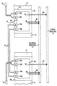
As shown in Figs. 2, one or more inventive interconnection modules, e.g., 16a
and 18b, are installed within shelves 12, 14, respectively, of distribution
frame 10 and
interconnected via jumper pair 52. Inventive interconnection modules 16a, 18b
include a
distributed intelligence arrangement (shown generally as 66) coupled to their
first (62)
and/or second (64) jack pairs. The arrangement enables operable connection
with an
CA 02212759 1997-08-12
9
electrical interconnection fabric (shown as 72) and an optical interconnection
fabric
(shown as 74) in addition to the conventional optical cross-connection between
optical
channel 32 and optical channel 42. Interconnection modules including
distributed
intelligence are interchangeable with conventional interconnection modules
and, except
for their distributed intelligence arrangement, have conventional structure.
Interconnection modules having distributed intelligence include a front face
76
having conventional jacks for optical cross-connection. Also, the inventive
interconnection modules each have a rear face 78 for operable connection to
interconnection fabrics 72, 74. For example, at least one optical jack 82 is
adapted for
optical connection to optical interconnection fabric 74 via an optical fiber
coupling 84
and at least one pair of electrical connectors 86 is adapted for electrical
connection of at
least the distributed intelligence portion 66 of the interconnection modules
to electrical
interconnection fabric 72 via wires 88.
In this inventive arrangement, interconnection modules within a shelf are
adapted
to be electrically coupled to a corresponding backplane arrangement or shelf
controller
interface (SCI) bus 91 which is electrically coupled to a corresponding shelf
controller or
shelf controller module (SCM) 92. Shelf controllers within a bay (e.g., a
group of
shelves) are electrically coupled via an interconnection bus 94 (e.g., a local
area network
or LAN bus) to a corresponding bay controller 95 (shown in Fig. 3). Likewise,
bay
controllers are electrically coupled to controller 90 through said
interconnection bus 94.
Shelf controllers 92 and bay controllers 95 typically take the form of
interconnection
modules or backplane arrangements and thus, in actual practice, are installed,
e.g., within
spare locations in existing shelves.
Optical connection between interconnection modules and controller 90 is
similar.
A plurality of optical switches function as controllers at the shelf, bay and
system levels
in a similar cascading scheme. For example, each shelf has an optical switch
102 for
CA 02212759 1997-08-12
optically coupling thereto the interconnection modules within that shelf.
Also, shelf
controlling optical switches 102 are optically coupled to an optical switch
104
corresponding to the bay within which the shelf is located. Each bay
controlling optical
switch 104 is optically coupled to a system optical switch 106 for optical
connection to
5 controller 90. Depending on the optical system arrangement, controller 90
can be a
frame controller providing a gateway between interconnection bus 94 and the
next higher
network level.
Referring to Fig. 3, an interconnection module according to an embodiment of
the invention is shown. Inventive interconnection module 16a has a plurality
of input
10 jacks 62a, 62b, 64a, 64b on front face 76 that are consistent with the
input jacks of
conventional interconnection modules, thus contributing to the
interchangeability of
interconnection module 16a with conventional interconnection modules. Such
interchangeability is a significant feature of the inventive interconnection
module.
Interconnection module 16a includes a first wavelength division multiplexes
(WDM) 124 with an input optically coupled to Rx jack 62a and an output
optically
coupled to an optical tap 126. One output of optical tap 126 is optically
coupled to Tx
jack 64b and the other output is coupled to a microcontroller 128 or other
suitable
device for interpreting the information collected by optical tap 126. For
example,
microcontroller 128 may have a light detecting component such as a photodiode
(not
shown) that converts the light coupled from optical tap 126 to an electrical
signal used
internally by microcontroller 128 or by an external passive device such as an
LED 134
coupled to microcontroller 128. Alternatively, microcontroller 128 may have
receiving
components capable of interpreting the optical information coupled from
optical tap 126.
As shown in Fig. 3, the microcontroller 128 is coupled to optical 126 by means
of
electronics 143 suitable for converting optical power to a corresponding
electrical
signal, as would be understood by a person skilled in the art. Also,
microcontroller 128
CA 02212759 1997-08-12
11
is electrically connected to electrical interconnection fabric 72 via an
electrical coupling
142.
Tx jack 62b is optically coupled to the output of a second WDM 144 (the
primary direction of optical transmission is depicted in Fig. 4 by arrows).
The first of
two inputs of second WDM 144 is optically coupled to optical interconnection
fabric 74
and the second input is optically coupled to the output of a third WDM 148.
The input
of third WDM 148 is optically coupled to Rx jack 64a. Alternatively, WDM 144
and/or
WDM 148 are suitable for an optical tap (not shown) to be coupled therewith,
where an
output of the optical tap would be coupled to the microcontroller 128 or
alternately an
additional microcontroller for monitoring the optical channel received on Rx
jack 64a.
Such a connection from Rx jack 64a is typically made from equipment within the
customer premises, however. In addition, it would be understood that the WDM
144
and WDM 148 may be combined into a single unit.
Optical filters may also be coupled at any of the interconnections to the jack
pairs, including the interconnection to the optical backplane at test ports,
to thereby
provide isolation protection for the interconnection module and other
equipment coupled
within the signal path. In one embodiment, the isolation filters 150, 152 are
coupled to
the (OSP) jack pairs and the test ports 160. An LED test button or switch 154
is also
coupled to the microcontroller 128 which when activated provides a
communication test
to the shelf controller module 92. The LED within the test button 154 acts as
an
indicator for a variety of functions, such as, fiber tracing or patching.
Another push-
button (switch) 156 may be activated in order to place the microcontroller 128
of an
individual interconnection module into a self-test diagnostic mode. LED 134
acts as a
fault indicator that illuminates when a fault has been detected, and also
reflects the status
of the module at any time.
CA 02212759 1997-08-12
12
In operation, an optical signal transmitted from first optical channel 32 is
received
by interconnection module 16a via Rx jack 62a. The optical signal is optically
coupled
to Tx jack 64b through first WDM 124 and optical tap 126. First WDM 124
separates
portions of the incoming optical signal, e.g., and transmits the desired
components to
optical tap 126. Optical tap deflects a small portion of the optical signal to
microcontroller 128 for monitoring, testing and/or other analysis. The
remaining portion
of the optical signal is transmitted to Tx jack 64b for subsequent optical
coupling to the
Rx jack (i.e., Rx jack 64a) of a cross-connected interconnection module (i.e.,
interconnection module 18b).
Microcontroller 128 is capable of continuously monitoring the content and/or
strength of the optical signal it receives from optical tap 126 to determine
if an
appropriate action needs to be performed. Also, because microcontroller 128 is
electrically connected via electrical interconnection fabric 72 to system
controller 90,
electrical information can be transmitted therebetween as needed.
For example, if microcontroller 128 determines that the strength of the
optical
signal it receives from optical tap 126 is questionable, such information can
be sent to
system controller 90 for necessary processing. In response thereto, for
example, system
controller 90 controls transmission of the appropriate optical test signals
through optical
interconnection fabric 74 and WDMs 142 and 144 to Rx jack 62a and/or Tx jack
62b of
the interconnection module that originally sent the information. Such test
signals
include, e.g., optical time domain reflectometry (OTDR) test signals in
accordance with
conventional OTDR principles. In this manner, the integrity of first optical
channel 32
and jacks 62a, 62b are enabled to be tested continuously and automatically. In
one
embodiment of the invention, test signals which are sent to the optical
channel in
question are of a different wavelength, e.g., 1550 nm, than are the typical
transmissions
over the optical channel, which may have a wavelength, for example, of 1310
nm.
CA 02212759 1997-08-12
13
Because microcontroller 128 is an actively intelligent device, it can be
configured
to include addressable functions. Thus, microcontroller 128 is suitable for
transmitting
electrical information containing address information identifying the source
of the
information (i.e., the interconnection module from which the information was
transmitted). Also, although an optical signal strength testing operation is
described
above, it is within the scope of the invention for microcontroller 128 to
analyze the
content of tapped optical information and to communicate with system
controller 90
over the established LAN accordingly. In this manner, microcontroller 128 is
capable of
incorporating control information, monitoring statistic information and other
content-based information initiated by microcontroller into the electrical
information
transmitted to system controller 90 or other interconnection modules.
The actively intelligent nature of the inventive interconnection modules
allows
them to be installed within existing non-intelligent distribution frames and
to become part
of the overall optical communications system. For example, a newly installed
interconnection module is capable of transmitting its identity, module type
and other
characteristic information to system controller 90 and to other
interconnection modules
within the optical communications system via electrical interconnection fabric
72.
Therefore, the overall configuration of the optical communications system is
capable of
being updated automatically upon installation of an inventive interconnection
module
therein.
Furthermore, it is within the scope of the invention for the distributed
intelligence
to cause an interconnection module to shift into a local operating mode or a
self
diagnostic mode in the event of a network emergency. The results of such
actions
include, for example, self healing in the form of rerouting the optical
connections of the
interconnection module in question. Also, continued operation in the event of
power
failure is possible through local operating modes.
CA 02212759 1997-08-12
14
Microcontroller 128 is capable of including therewith other sensing and/or
testing
equipment, and is capable of incorporating information in addition to that
transmitted via
Rx jack 62a. For example, microcontroller 128 can include or be replaced by a
sensor
that determines the temperature and/or quality of the air surrounding
interconnection
module 16a. Such information can be used in monitoring and/or testing
functions. Also,
microcontroller 128 is capable of being configured to analyze previous
monitoring
information and to perform statistical performance monitoring based on such
information. In this manner, the interconnection modules are actively
performing failure
prediction functions instead of passively reacting to an established threshold
condition.
Other functions adaptable for use by microcontroller 128 in this regard
include fiber
tracing, protection line switching, monitoring the surrounding environment.
All of these
functions, as well as those discussed herein previously, are capable of
performance in
both single mode and mufti-mode optical fiber.
As discussed previously, the characteristically branched electrical and
optical
interconnection fabrics 72, 74 allow the distribution frames within an optical
communications system to be monitored automatically. Also, the distributed
intelligence
allows most if not all of the monitoring, processing and the like to be
performed locally
(i.e., at the interconnection modules) through, for example, distributed
parallel
processing, rather than passively transmitting the information from the
interconnection
modules to a remotely located system controller.
For example, assuming interconnection module 1 6a is optically connected to
the
first optical channel and cross-connected with interconnection module 18b,
which is
assumed to be optically connected to the second optical channel, the
distributed
intelligence installed in each interconnection module is used to monitor the
operation and
maintenance of that optical communication channel. First, several if not all
SCMs 92
electrically polls, in real time, the interconnection modules within its
respective shelf for
any information such as monitoring status. This simultaneous polling
epitomizes the
CA 02212759 1997-08-12
distributed or massive parallel processing effort of the invention. Unlike,
conventional
systems (which use one shared polling device to obtain information serially on
a fiber by
fiber basis, resulting in non-real-time results and long duty cycles), the
distributed
intelligence does not require polling type sharing and thus does not affect
the
responsiveness of the system. Thus, communication systems using massive
parallel
processing techniques are not limited by the number of optical fiber channels
operating
therein.
In the event an SCM receives a positive status report from an interconnection
module (i.e., a flagged event has occurred at the interconnection module),
information
10 concerning the flagged event, the interconnection module originating the
flagged event
and any control information for responding appropriately to the flagged event
is
transmitted from the respective SCM to system controller 90. Once the
information has
been received, appropriate information or test signals can be transmitted from
system
controller 90 to the interconnection module from which the information was
received.
15 Alternatively, information and/or test signals can be transmitted to the
interconnection
module that is cross-connected to the interconnection module from which the
flagged
event information was sent. In this manner, the entire optical communiaations
system is
monitored simultaneously and tested automatically when necessary or requested.
Refernng to Figs. 4-6, in combination with one another, there are shown
perspective, side and rear views, respectively, of one advantageous embodiment
illustrating the physical design for the present invention interconnection
module 16a. As
can be seen, located on a front faceplate 76 of the module, there is included
a first jack
pair 62 (Rx jack 62a and Tx jack 62b) adapted to receive and interconnect with
conventional fiber optic cables, for example, OSP connections. A second jack
pair 64
(Rx jack 64a and Tx jack 64b) is also located on the faceplate, for example,
for making
equipment connections to conventional fiber optic cables. Additionally, the
module
includes a third jack pair 160 (Rx 160a and Tx 160b) for making test
connections, for
CA 02212759 1997-08-12
16
example, to the optical backplane 74 and for use with an OTDR, as described
with
respect to Fig 3. An electrical port 162 is also included for making
electrical connections
to the electrical backplane 72. As shown, the electrical port 162 is adapted
to receive a
ribbon connector 164, although it will be understood that any other type of
conventional
electrical connector may also be used. The interconnection module also
includes an LED
test button 154 shown at the top of the module which as previously described
provides a
communication test to the shelf controller. The LED within the test button 154
acts as an
indicator for a variety of functions, such as, fiber tracing or patching.
Another push-
button 156 may be activated in order to place the microcontroller of an
individual
interconnection module into a self-test diagnostic mode. LED 134 acts as a
fault
indicator that illuminates when a fault has been detected, and also reflects
the status of
the module at any time.
The present invention module 16a is preferably dimensioned so that the module
fits within the allotted shelf space of an existing fiber optic distribution
shelf, where fiber
distribution shelves typically come in standard sizes, for example, having
heights of five,
seven or nine inches. In this way, the modules are easily retrofitted into the
shelving of
also existing fiber optic distribution frames which is a significant advantage
to the present
invention. As shown, push pins 166 are included on the faceplate 76 of the
module in
order to mechanically couple to the shelf of distribution frame.
Referring to Fig. 7, the module as illustrated is demonstrative of additional
advantageous feature of the present invention. As shown, the module is
separable and
can be decoupled into two sub-modules, an optical sub-module 172 and an
electronic
sub-module 174, where each sub-module is partitioned into a separate housing.
The
optical sub-module 172 includes all of the optical connector inputs and
outputs, e.g., the
jack pairs, along with the optical tap and WDM devices. The electronics sub-
module
174 includes the electronic components, e.g., the microcontroller, used for
converting
CA 02212759 1997-08-12
17
the optical signal into an electronic signal and the electronics for
processing and relaying
the electronic signal to the backplane and into the LAN.
The two sub-modules are optically coupled to one another by means of a blind
mate optical coupler 180, although other known optical coupling devices may
also be
used. As shown, the optical sub-module includes a male 182 end of the blind
mate
coupler, while the female end (not shown) is included on the electronics sub-
module. As
would be understood, the mating arrangement of the coupler, i.e., male and
female,
could also be reversed for the two sub-modules. Proper mating of the optical
coupler
and thus the two sub-modules is ensured by rails 184 on the top and bottom of
the
electronics sub-module which slidably engage corresponding guides 186 on the
optical
module when the two sub-modules or module halves are mated together. The
guides 186
and rails 184 ensure that the male and female ends of the optical coupler 180
will align
when the two modules are joined using the shown sliding arrangement. It would
also be
understood, however, that other well-known guides and mating arrangements any
also
be used to ensure proper coupling of the two sub-modules.
As shown, the electronics sub-module 174 when mated with the optical sub-
module 172 is disposed within an inset 190 on the faceplate 76 of the optical
module.
Accordingly, when the two sub-modules are mated together the combination
appears as
a single interconnection module. The two sub-modules are then held in place as
a single
module by the tightening of a single screw 192 which is fastened through a
bracket edge
194 of the optical sub-module 172 which engages the electronics sub-module
174. The
two-part combination interconnection module is advantageous in that the
optical
connector inputs and outputs can be completely decoupled from the electronics
and vice
versa. Typically a channel failure that is isolated to be within the
interconnection module
itself will be either part of the optical or the electronics arrangement, but
not both. In
this way if an interconnection module fails, by way of the present invention,
the failure
can be easily isolated between the optical and electronic sub-module (for
example, by
CA 02212759 1997-08-12
1g
attempting replacement of either sub-module) and only one of either of the two
sub-
modules will need replacement to remedy the channel failure. As would be
understood
this is a significant advantage in terms of cost savings for properly
maintaining the
optical communications network.
From the above, it should be understood that the embodiments described, in
regard to
the drawings, are merely exemplary and that a person skilled in the art may
make variations
and modifications to the shown embodiments without departing from the spirit
and scope of
the invention. All such variations and modifications are intended to be
included within the
scope of the invention as defined in the appended claims.