Note: Descriptions are shown in the official language in which they were submitted.
CA 0221276~ 1997-08-08
W O 96/24953 PcT/
TRENCH FIELD EFFECT TRANSISTOR WITH REDUCED
PUNCH-THROUGH SUSCEPTIBILITY AND LOW RD~
FIELD OF THE lNV~N~l'lON
This invention relates to trench field effect
transistors.
BACKGROUND INFORMATION
10Figure 1 (Prior Art) is a simplified cross-
sectional diagram of a conventional planar double
diffused field effect transistor. A layer of N type
epitaxial silicon 1 is formed on an N+ type substrate
2. A P body region 3A and a P+ body region are formed
into the epitaxial layer from upper surface 4, and an
N+ type source region 5 is formed into the body regions
3A and 3B from upper surface 4. To turn the transistor
on (i.e., make it conductive), a positive potential is
placed on gate 6. The positive potential on gate 6
causes what is called a channel region to form in the
surface portion of P body region 3A underneath the gate
and also causes what is called an accumulation region
to form in the surface portion of the N type epitaxial
silicon region lA ; ~~;ately underneath the gate.
Electrons can then flow as generally indicated by the
arrow from the N+ type source region 5, through the
channel region in P body region 3A, through the
accumulation region of N type epitaxial layer lA,
downward through the N type epitaxial region lA,
downward through the N+ type substrate 2, and to a
drain electrode 7. If gate 6 does not have a positive
potential, then no channel is formed and no electron
flow from source to drain takes place. The transistor
is therefore turned off (i.e., nonconductive).
Figure 2 (Prior Art) is a simplified cross-
sectional diagram of another type of double diffused
field effect transistor, a trench field effect
CA 0221276~ 1997-08-08
W 096124953 PCTAUSg~
transistor. An N type epitaxial layer 1 is formed on a
N+ type substrate 2. Body regions 3A and 3B and N+
type source region 5 are then formed in similar double
diffused fashion to the body and source regions in the
planar transistor. In the case of the trench
transistor, a trench is etched down into epitaxial
layer 1 from upper surface 4. A gate oxide layer 8 is
then grown in this trench on the side walls and the
trench bottom. An amount of polysilicon or other
suitable material is then deposited on the gate oxide
in the trench to form a gate 9. For additional
information on trench field effect transistors, see
U.S. Patent No. 5,072,266 entitled "Trench DMOS Power
Transistor With Field-Shaping Body Profile And Three-
Dimensional Geometry", the subject matter of which isincorporated herein by reference.
To turn the trench transistor on, a positive
potential is placed on gate 9. The positive potential
causes a channel region to form in the portion of the P
body region 3A which forms part of the sidewall of the
trench and causes an accumulation region to form in the
portion of the N type epitaxial layer region lA which
forms a part of the sidewall of the trench. Electrons
can then flow as indicated by the arrow from the N+
type source region 5, downward through the channel
region of P body region 3A, downward through the
accumulation region, downward through the remainder of
the N type epitaxial region lA, downward through the N+
type substrate 2, and to a drain electrode 7. If gate
9 does not have a positive potential, then no channel
is formed and no electron flow from source to drain
takes place. The transistor is therefore turned off.
It is desirable that such transistors have low
source-to--drain resistances RDSOr~ when turned on. As
depicted pictorially in Figure 1, the resistance RDSO~ in
the planar structure is made up of the resistance RcH
CA 0221276~ 1997-08-08
W O 96/24953 PCTAUS95'~Gg11
through the channel, the resistance RACC laterally
through the accumulation region, the resistance RJFET
vertically through the pinched portion of the N type
epitaxial region lA between the two adjacent P body
regions, the resistance RD~FT vertically through the
remainder of the N type epitaxial region lA to the
substrate, and the resistance Rs~ vertically through
the substrate to the drain electrode. As depicted
pictorially in Figure 2, the resistance RDS~ in the
trench structure is made up of the resistance RCH
vertically through the channel, the resistance RACC
vertically through the accumulation region, the
resistance RD~FT vertically through the remainder of the
N type epitaxial region lA, and the resistance R
vertically through the substrate to the drain
electrode. Note that RJFET is eliminated in the trench
device. Because the conductivity of silicon increases
with dopant concentration, epitaxial silicon layer 1 is
relatively heavily doped to reduce the RD~FT and thereby
reduce RD~ -
It is also desirable that such transistors notsuffer what is called "punchthrough". When a high
voltage is placed across the transistor from the source
to the drain such as when the transistor is off in a
high voltage application, a depletion region will form
along the N+ type source to P body junction.
Similarly, a depletion region will form along the P
body to N type epitaxial layer region junction. If the
source-to-drain voltage is high enough, the depletion
regions will extend so far inward into the P body
region 3A that they will meet. This is called
punchthrough. As a result, an undesirable conductive
path is formed through the P body region 3A when the
transistor should be off.
A power field effect transistor is sought which
has both low RDS~ as well as the ability to withstand
CA 0221276~ 1997-08-08
W 0961249S3 PCTrUS9GI'~0941
high source-to-drain voltages without suffering
punchthrough problems.
SUMMARY
To reduce susceptibility to punchthrough, the
channel region of the P body region of a trench field
effect transistor is formed in a layer of lightly doped
epitaxial silicon. As a result, the channel region has
less counterdoping from the background N type epitaxial
silicon dopants and has a greater net P type dopant
concentration. Due to the higher net P type dopant
concentration of the P body region, the depletion
regions on either side of the P body region expand less
far inward through the P body region at a given
voltage, thereby rendering the transistor less
susceptible to source-to-drain punchthrough.
To maintain a low RD~ the relatively high
conductivity of an accumulation region formed along a
sidewall of the trench of the transistor when the
transistor is on is used to form a conductive path from
the channel region to an underlying relatively highly
conductive layer upon which the lightly doped epitaxial
layer is formed. This underlying relatively highly
conductive layer may, for example, be either substrate
or a more heavily doped epitaxial silicon layer. Some
embodiments have low threshold voltages (such as 0.6 to
1.0 volts) and are usable in low voltage battery
applications (2.5 to 3.3 volts). Other details of
structures and associated methods are also disclosed.
BRIEF DESCRIPTION OF THE DRAWINGS
Figure 1 (Prior Art) is a cross-sectional diagram
of a planar double diffused field effect transistor.
Figure 2 (Prior Art) is a cross-sectional diagram
of a trench double diffused field effect transistor.
Figure 3 is a simplified cross-sectional diagram
CA 0221276~ 1997-08-08
W 096124953 PCTAU596/~o9
of a planar double diffused field effect transistor.
Figure 4 is a simplified cross-sectional diagram
of a trench double diffused field effect transistor
formed in a double epit~ layer structure in
accordance with another embodiment of the present
invention.
Figure 5 is an approximate dopant profile taken
along line A-A of Figure 4.
Figure 6 is a simplified cross-sectional diagram
of a trench double diffused field effect transistor
formed in a single epitaxial layer structure in
accordance with yet another embodiment of the present
invention.
Figure 7 is an approximate dopant profile taken
along line B-B of Figure 6.
DETATT~n DESCRIPTION OF THE PREFERRED EMBODIMENTS
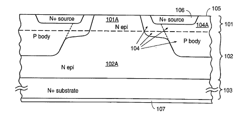
Figure 3 is a simplified cross-sectional diagram
of a planar double diffused field effect transistor. A
lightly doped N- type epitaxial layer 101 is disposed
on a more heavily doped-N type epitaxial layer 102
which is in turn disposed on a more heavily doped N+
type substrate layer 103. A P body region 104 is
formed into the epitaxial layers 101 and 102 from upper
surface 105 to form a relatively heavily doped
epitaxial region 102A and a relatively lightly doped
epitaxial region 101A. (As indicated by the dashed
line, "P body region" 104 is understood to entail a
relatively lightly doped doubly diffused portion and a
more highly doped body portion which correspond with
regions 3A and 3B of Figure 2, respectively. The
dashed lines in Figures 4 and 6 similarly indicate that
each of those P body regions actually comprises a
relatively lightly doped portion and more highly doped
portion.)
N+ type source region 106 is then formed into P
CA 0221276~ 1997-08-08
W O 96/24953 PCT~US9G~ 9~1
body region 104 from upper surface 105. The drain 107
is located on the underside of the substrate 103. The
conventional gate (as in Figure 1) and contacts and
other possible layers are not illustrated to improve
the clarity of the diagram. Relatively lightly doped
N- type epitaxial layer 101 can be either an ion
implanted counterdoped portion of layer 102 or it can
be grown having its relatively light dopant
concentration.
A depletion region expands less far for a given
voltage in a relatively heavily doped silicon than it
would for that given voltage in a relatively lightly
doped silicon. Accordingly, the upper portion 104A (in
which the channel region is disposed) has a higher net
doping. The relatively lightly doped epitaxial silicon
layer 101 is provided so that there will be less
background counterdoping of the P body dopants in upper
portion 104A. Accordingly, the region 104A of the P
body region has a higher net doping concentration and
the depletion regions do not punchthrough as easily
from source region 106 to region 101A. Furthermore, to
maintain a low RDSO~ the resistance RDR~ is maintained at
a low value due to the use of the relatively heavily
doped epitaxial layer 102. Both improved punchthrough
resistance as well as low RDSO~ is therefore achieved.
For additional information pertaining to such a
structure, see U.S. Patent Appl. Ser. No. 08/131,114
entitled "Low Threshold Voltage Epitaxial DMOS
Technology", the subject matter of which is
incorporated herein by reference.
The structure of Figure 3, however, involves the
higher resistances through the relatively lightly doped
N- epitaxial layer region 101A. The structure of
Figure 3 is disclosed in the copending application
serial number 08/131,114, the subject matter of which
is incorporated herein by reference. To eliminate
--6--
CA 0221276~ 1997-08-08
W 096124953 PCTrUS9~ 9~1
these high resistances of region lOlA in the path the
drain-to-source current, the structure of Figure 4 is
provided.
v Figure 4 is a simplified cross-sectional diagram
5 of a trench double diffused field effect transistor
which does not incur the resistance penalty that the
transistor of Figure 3 does. A lightly doped N- type
epitaxial layer 201 is disposed on a more heavily doped
N type epit~xi~l layer 202 which is in turn disposed on
10 a more heavily doped N+ type substrate layer 203. A P
body region 204 is formed into the epitaxial layers 201
and 202 from upper surface 205 to form a relatively
heavily doped epitaxial region 202A and a relatively
light doped epitaxial region 20lA. N+ type source
region 206 is formed into P body region 204 from upper
surface 205. The drain 207 is located on the underside
of the substrate 203. Relatively lightly doped N- type
epitaxial layer 201 can be either an ion implanted
counterdoped portion of epitaxial layer 202 or it can
20 be grown having its final relatively light dopant
concentration. A trench is etched into surface 205 and
a gate oxide 208 and gate 209 are formed as in the
trench transistor structure of Figure 2. See U.S.
Patent No. 5,072,266, the contents of which are
25 incorporated herein by reference, for details on
fabricating a trench field effect transistor.
The structure of Figure 4 does not incur the
resistance penalty associated with the planar structure
of Figure 3 because electron flow proceeds through the
30 N- type epitaxial region 201A in an accumulation region
along the sidewall of the trench. The resistance in an
accumulation region is substantially independent of
dopant concentration. The gate/trench structure
therefore forms a means for controllably forming the
35 accumulation region. After the electrons have passed
through the N- type epitaxial region 201A, the
CA 0221276~ 1997-08-08
W 096/24953 , , PCTAUSg~'~Og11
electrons pass through the relatively heavily doped N
type epitaxial region 202A where the resistance is also
low.
Figure 5 is a diagram showing an approximate
dopant profile along the line labeled A-A in Figure 4.
The 3-9E15 dopant concentration is the approximate
dopant concentration of the relatively lightly doped N-
type epitaxial region 201A of Figure 4. The net peak
doping concentration in the channel region of P body
region 204 is 3-9E16. Dopant concentrations are in
atoms/cm3.
Figure 6 is a simplified cross-sectional diagram
of a trench double diffused field effect transistor in
accordance with another embodiment of the present
invention. The gate region 209A extends into the N+
type substrate 203. Only one epitaxial layer, a
relatively lightly doped N- type epitaxial layer 201,
is used. Electrons flow vertically in the low
resistance accumulation region at the sidewall of the
trench from the low resistance channel region in P body
region 204 downward to the N+ substrate 203. A
specific RDSO~ in the range of O.1 to 0.5 ohms-cm2 is
achievable in a device having a breakdown voltage in
the range of 15 to 30 volts and a threshold voltage in
the range of 0.6 to 1.0 volts.
Figure 7 is a diagram showing an approximate
dopant profile along the line labeled B-B in Figure 6.
The 3-9E15 dopant concentration is the dopant
concentration of the relatively lightly doped N- type
epitaxial region 201A of Figure 6. Due to the heavily
doped N+ type substrate 203 being in close proximity to
gate 209A, a relatively high electric field develops
between gate 209A and N+ substrate 203 as compared to
the electric field developed between gate 209 and N
type epitaxial region 202A of Figure 4. The net P type
peak doping concentration in the channel region of P
CA 0221276~ 1997-08-08
W O 96t24953 , PCTrUS~ 341
type body region ~04 is 3-9E16.
The structure of Fsigure 6 has the advantage of not
requiring the double epitaxial layer structure in
relatively low source-to-drain voltage applications
(such as 12-30 volts). The structure of Figure 4, on
'J the other hand, is usable in relatively high source-to-
drain voltage applications (up to approximately 60
volts).
Approximate thickness ranges for the embodiment of
Figure 4 are 0.5 microns for source region 206, 1.0-2.0
microns for P body region 204 at the trench sidewall,
1.0-3.0 microns from the bottom of the P body region at
the sidewall to the top of N+ substrate layer 203. The
gate oxide may, for example, be 150-1000 angstroms
thick. The trench may be, for example, 1.2-2.0 microns
deep. Epitaxial layers 201 and 202 may be a combined
4.0-12.0 microns thick. The short channel renders the
transistor usable in low threshold voltage applications
such as battery applications.
Approximate thickness ranges for the embodiment of
Figure 6 are 0.5 microns-for source region 206, 1.0-2.0
microns for P body region 204 at the trench sidewall,
1.0-2.0 microns from the bottom of the P body region at
the sidewall to the top of N+ substrate layer 203. The
gate oxide may, for example, be 150-1000 angstroms
thick. The trench may be approximately 1.2-6.0 microns
deep. The bottom of the trench may be approximately
0.5-1.0 microns from the top of N+ type substrate layer
203. Epitaxial layer 201 may be approximately 2.0-5.0
microns thick. The short channel renders the
transistor usable in low threshold voltage applications
such as battery applications.
Although the invention is described in connection
with certain illustrative embodiments for instructional
purposes, the invention is not limited thereto.
Thicknesses, structural contours, and dopant
:~ :
CA 0221276~ 1997-08-08
W 096/24953 PCTAUS~/A~9~1
concentrations may be altered. Other layers and other
structures may be added. The invention is applicable
to transistors other than double diffused transistors.
Both N channel and P channel transistors are realized
in accordance with the present invention. Accordingly,
modifications, adaptations, and combinations of various
aspects of the specific embodiments can be practiced
without departing from the scope of the invention as
set forth in the following claims.
--10--