Note: Descriptions are shown in the official language in which they were submitted.
CA 02212821 1997-08-12
1
HIGH STABILITY SINGLE-PORT SAW
RESONATOR OSCILLATOR
BACKGROUND OF THE INVENTION
1. FIELD OF THE INVENTION
The present invention relates in general to oscillators and in particular
to a high stability oscillator having a single-port resonator coupled between
the
base of a transistor and ground and that has an output circuit for providing
complementary outputs and that is highly stable with environmental and
S component changes and has particular value as a clock oscillator.
DLMAIN Doc: 210828 1
CA 02212821 1997-08-12
2
2. DESCRIPTION OF RELATED ART INCLUDING
INFORMATION DISCLOSED UNDER 37 CFR 1.97 AND 1.98
High frequency oscillators are used for a number of purposes. Among
these purposes is to generate clock pulses for use in computer processing
systems and the like. Obviously such clocks must be very accurate and not
subject to substantial instability.
There are different constructions of such oscillators, one of which is
illustrated in FIG. 1. The oscillator 10 has a transistor 12 with a capacitor
14
coupled between the emitter and ground 18 to cause oscillations by making the
circuit unstable. The coil 16, as is well known, has a low Q value (i.e. 50)
and
defines the frequency of oscillation. The output oscillations are coupled
through resistor 20 and across load resistor 22 to form the output at line 24.
This circuit has several disadvantages. First, it has a very wide bandwidth
and,
second, it is too unstable to be used as a clock pulse generator. FIG. 2 is a
graph illustrating the range of oscillation of the circuit 10. As is well
known,
for the circuit to operate, at the point of oscillation the resistance at the
ground end of coil 16 must be negative and the reactance must be zero. It will
be noted that while the resistance 15 is negative, the reactance is zero for a
wide range that could be in the order of 150 kilohertz. The range of
oscillation during this period is known as fitter and causes the circuit of
FIG. 1
to be unusable for a high frequency clock pulse generator because of its
instability.
FIG. 3 is an example of another prior art clock oscillator circuit that
produces complementary outputs Q and Q. Circuit 26 is a coupled resonator
oscillator and utilizes two matched surface acoustic wave devices 28 and 30 on
the input and output, respectively, of the circuit 26. This circuit is quite
stable;
however, it has several disadvantages. First, it has to have matched surface
DLMAIN Doc: 210828 1
CA 02212821 1997-08-12
3
acoustic wave (SAW) devices on the input and output to get the maximum
output power. The formation of such SAW devices is very expensive. Further,
each is a two-port resonator which also increases the cost of the SAW devices.
FIG 4 is a block diagram of an AC representation of a Colpitts family of
oscillators. The circuit 25 includes a ground line 23 surrounding the
oscillator
circuit. When the collector, c, of transistor 27 is coupled to ground 23 as
indicated by phantom line 29, a conventional Colpitts oscillator is formed.
When the emitter, e, of transistor 27 is coupled to ground 23 as indicated by
phantom line 33, a Pierce oscillator is formed. Finally, when the base, b, of
transistor 27 is coupled to ground 23 as indicated by phantom line 31, a Clapp
oscillator is established. In each of these cases, either the collector, the
emitter, or the base of the transistor 27 is grounded. Thus, each of these
circuits requires an inductor, (Z3), in the external circuit, (Zl and ZZ being
capacitors). This inductor is costly and absorbs RF power. See a further
discussion of these circuits in Parzen, "Design of Crystal and other Harmonic
Oscillators", 1983, John Wiley and Sons.
Thus, there is a need for an oscillator that is economical to construct,
easy to assemble, has high stability over a wide range of environmental
changes, load changes, and component value changes. Further, such oscillator
should produce complementary outputs that are 180° out-of-phase with
each
other.
DLMAIN Doc: 210828 1
CA 02212821 1997-08-12
4
SUMMARY OF THE INVENTION
By using a circuit similar to the circuit in FIG. 1 but utilizing a single-
port resonator coupled between the transistor base and ground with a
capacitor coupling the base to the emitter, an oscillator is obtained that has
very high stability, is easy to construct and can be utilized on a single chip
as
an integrated circuit, and which is economical to construct.
Thus, it is an object of the present invention to provide a high stability
oscillator that can be used for a clock pulse generator.
It is also an object of the present invention to provide a high stability
oscillator that utilizes a single-port resonator surface acoustic wave device
to
establish the frequency of oscillation of the oscillator.
It is still another object of the present invention to provide a high
stability oscillator that may or may not have an enable port.
It is yet another object of the present invention to provide a high stability
oscillator that has a balun on the output thereof for converting the single
output to complementary outputs.
Thus, the present invention relates to a single-port high stability
resonator oscillator comprising a transistor having a base, an emitter, and a
collector, the collector providing an oscillator output signal; a single-port
resonator coupled between the transistor base and a ground potential; first
and
second series connected capacitors coupled between the transistor base and
the ground potential; a first resistor having a first end coupled to both the
transistor emitter and to the connection between the capacitors and a second
end coupled to the ground potential; and a second resistor having a first end
connected to the transistor base and a second end connected to a power
source for providing a bias to the base and collector of the transistor. If
desired, a third resistor having a first end connected to the transistor base
and
DLMAIN Doc: 210828 1
CA 02212821 1997-08-12
a second end connected to ground potential may be used as a basic
arrangement. It is to be understood that the invention also includes all known
methods in the state of the art for biasing the base and/or collector of the
transistor. The invention also includes a balun output circuit having a single
5 input coupled to the transistor collector and a balanced output for
generating
true and complement oscillator output signals.
The invention also broadly relates to an inductorless oscillator having a
stability greater than the stability of an oscillator circuit having an
inductor
therein, the inductorless oscillator comprising a transistor having a base, an
emitter, and a collector; a single-port SAW resonator coupled between the
transistor base and ground, the SAW having a Q value greater than that
achievable with the oscillator circuit having the inductor therein; and an
electrical circuit coupled to the transistor such that each of the transistor
base,
emitter, and collector terminals are isolated from ground potential.
DLMAIN Doc: 210828 1
CA 02212821 1997-08-12
6
BRIEF DESCRIPTION OF THE DRAWINGS
These and other features of the present invention will be more fully
disclosed when taken in conjunction with the following DETAILED
DESCRIPTION OF THE PREFERRED EMBODIMENTS in which like
numerals represent like elements and in which:
FIG. 1 is a circuit diagram of a prior art high frequency oscillator;
FIG. 2 is a graph of the oscillation fitter or instability of the
oscillator of FIG. 1;
FIG. 3 is a circuit diagram of a prior art coupled resonator
oscillator producing complementary outputs;
FIG.4 is a general circuit diagram illustrating the AC
representation of the Colpitts family of oscillators including the
conventional
Colpitts, the Pierce, and the Clapp oscillators;
FIG. 5 is a circuit diagram of the novel high stability oscillator of
the present invention;
FIG. 6 is a graph illustrating the range of fitter of the novel circuit
illustrated in FIG. 5;
FIG. 7 is a circuit diagram of an alternate embodiment of the novel
high stability of the present invention; and
FIG. 8 is a graph illustrating the high stability of the novel circuit
of FIG. 7 because of the narrow range of fitter.
DLMAIN Doc: 210828 1
CA 02212821 1997-08-12
7
DETAILED DESCRIPTION OF THE PREFERRED EMBODIMENTS
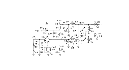
In FIG. 5, the novel inductorless oscillator circuit 36 includes a transistor
38 having a single-port surface acoustic wave resonator 40 coupled to the base
thereof to define the frequency of oscillation of the oscillator in circuit
36.
The transistor 38 may be a bipolar transistor of the type such as the NE856
series. Single-port SAW resonators are well known in the art. Such resonator
has a very high Q as is well known in the art, in the order of 5000, which
gives
great stability to the oscillator. SAW devices with a Q above 5000 could also
be used to provide high stability by changing other component values. The
SAW device 40 never resonates with any of the circuit elements so that the
base of transistor 38 is never grounded with respect to AC as is the Colpitts
family of oscillator circuits shown in FIG. 4. Capacitor 42 causes the
transistor
38 to become unstable and thus oscillate. Capacitor 44 increases the gain at
low frequency and does not have to be in the circuit at high frequencies
because the value of capacitor 44 decreases with an increase in frequency.
Resistor 46 is a bias resistor for the emitter of transistor 38. Resistors 48,
50,
and 52 form a voltage divider circuit for providing the necessary power or
bias
to the base of transistor 38 to allow operation of the circuit 36. Power
supply
voltage on line 54 is coupled to the resistors 48, 50, and 52. An enable
signal
may be applied to a line 56 to add sufficient bias to enable circuit 36 at a
particular instant in time and also includes a noise filter comprised of
resistor
35 and capacitor 37. A power supply filter 57 includes a resistor 58,
capacitor
60, and coil 62 coupled as shown. Thus, the oscillator alone in oscillator
circuit 36 is inductorless.
The output of the oscillator from transistor 38 on the collector is a single
output (line 39) isolated by transistor 38 from the rest of the circuit and is
DLMAIN Doc: 210828 1
CA 02212821 1997-08-12
8
coupled to a first filter 63 that comprises a capacitor 64, coil 66, and
capacitor
68 arranged in a pi network shape.
Thus the high stability single-port SAW resonator oscillator itself
comprises a transistor 38 having a base, an emitter, and a collector with the
collector providing an isolated oscillator output signal on line 39 to the pi
network 63. The single-port resonator 40 is coupled between the base of
transistor 38 and a ground potential 41 and never grounds the base of
transistor 38 during oscillator operation. First and second series coupled
capacitors 42 and 44 are coupled between the transistor base and the ground
potential 41. A first resistor 46 has a first end 47 coupled to a junction 43
between the capacitors 42 and 44 and the emitter of transistor 38, and a
second end 49 coupled to the ground potential 41. A second resistor 52 has
a first end 53 connected to the transistor base and coupled to a power supply
and a second end 55 connected to the ground potential 41. A balun output
circuit 51 has a single input 39 coupled to the transistor collector and a
balanced output 76 and 84 for generating true and complementary oscillator
output signals.
The first filter 63 of balun 51 has an input 39 connected to the collector
of transistor 38 and an output 59. The first filter 63 includes first and
second
capacitors 64 and 68 each having a first end 65 and 71, respectively, and a
second end connected to ground potential 41. A first inductor 66 has a first
end coupled to both the collector of transistor 38 on line 39 and the first
end
65 of capacitor 64. The second end of the first inductor 66 is coupled to the
first end 71 of the other capacitor 68 and forms a single line output
frequency
at line 59 from the oscillator transistor 38.
The balun circuit includes second and third filters 69 and 77 coupled in
parallel with each other and each has a first end forming an input that is
coupled to the single output of the first filter 63 on line 59.
DLMAIN Doc: 210828 1
CA 02212821 1997-08-12
9
Filter 69 has an inductor 70 with one end coupled to the single output
of filter 63 on line 59 and a second end coupled to capacitors 72 and 74.
Capacitor 72 has the other end coupled to ground and capacitor 74 has the
other end as the complementary output on line 76.
The third filter 77 has a capacitor 78 with one end coupled to the line 59
and the other end coupled to a coil 80 and a capacitor 82. The other end of
the coil 80 is connected to ground and the other end of capacitor 82 forms the
output on line 84 and is of the opposite phase from that on line 76. The
output on line 84 may be Q and the output on line 76 may be Q. Thus, these
two signals are 180 ° apart, one being a 90 ° + and the other 90
°-.
It can be seen from FIG. 6 that this circuit has excellent fitter
characteristics. Note, that the range of oscillation where the reactance of
the
circuit is zero is a very narrow 15 kilohertz. Thus, the circuit is highly
stable
and can be used for highly accurate clock pulses.
FIG. 7 illustrates an alternate version of the present invention wherein
the output of the oscillator circuit 86 is taken from the emitter of the
transistor. In this particular case, the oscillator circuit 86 includes a
transistor
88 having a surface acoustic wave device 90 coupled between the base of
transistor 88 and ground 93. In addition, capacitor 92 causes the circuit to
become unstable and enables the circuit to oscillate. Capacitor 94 again
increases the gain at low frequencies. The SAW device 90 determines the
frequency of oscillation. The output is taken across load resistor 96 on line
98.
In this particular oscillator, the collector is coupled to ground through
capacitor 100 thus forming an AC ground for the collector. The balun 51 of
FIG. 5 could be used with this embodiment to provide true and complement
outputs. Again, no inductor is required in the oscillator circuit itself.
DLMAIN Doc: 210828 1
CA 02212821 1997-08-12
1~
FIG. 8 is a graph illustrating the narrow fitter bandwidth of three
kilohertz for this circuit. Thus, it is a highly stable circuit and has
application
in high frequency circuits as a clock oscillator.
The corresponding structures, materials, acts, and equivalents of all
means or step plus function elements in the claims below are intended to
include any structure, material, or act for performing the function in
combination with other claimed elements as specifically claimed.
DLMAIN Doc: 210828 1