Note: Descriptions are shown in the official language in which they were submitted.
CA 0221297~ 1997-08-13
TITLE OF THE INVENTION
OPTICAL WAVELENGTH MULTIPLEXER/DEMULTIPLEXER
FIELD OF THE INVENTION
This invention relates to an optical wavelength
multiplexer/demultiplexer utilizing an arrayed-waveguide grating,
and more particularly to, an optical wavelength multiplexer/
demultiplexer in which each optical signal emerging from each
output channel waveguide has a reduced loss difference from each
other.
BACKGROUND OF THE INVENTION
In an optical communications field, wavelength-division
multiplexing (WDM) transmission systems have been studied for
enhancing information capacity. In these systems, a plurality of
optical signals at different wavelengths which are spaced by about
1 nm are transmitted over a single optical fiber. For this purpose,
an optical wavelength multiplexer/demultiplexer is an important
component which plays a significant roll to combine or separate the
optical signals at different wavelengths. Particularly, one of the
most promising optical wavelength multiplexer/demultiplexers for
such use is one which utilizes an arrayed-waveguide grating, which
may increase the number of multiplexed signals with relatively
narrow wavelength spacings.
One of conventional optical wavelength multiplexer/
demultiplexers is disclosed in Japanese Published Patent Application
No.4-163406.
CA 0221297~ 1997-08-13
The conventional optical wavelength multiplexer/
demultiplexer comprises at least one input channel waveguide for
receiving wavelength divislon multiplexed signals, the wavelength
division multiplexed signal comprising a plurality of signals having
a predetermined wavelength difference from each other, an input
slab waveguide for expanding the wavelength division multiplexed
signals coupled from the input channel waveguide into the input slab
waveguide, an arrayed-waveguide grating comprising a plurality of
channel waveguides, each channel waveguide having a predetermined
length difference in accordance with the predetermined wavelength
difference, so that each signal at different wavelength coupled to
and traveling over each channel waveguide is provided with a phase
difference from each other in accordance with the predetermined
length difference, an output slab waveguide for focusing the
signals at different wavelength coupled from the channel waveguides
into a plurality of predetermined positions in accordance with the
predetermined wavelength difference, respectively, and a plurality
of output channel waveguides, an input end of each output channel
waveguide being arranged at each predetermined position, so that
each separated signal at each wavelength is coupled to each output
channel waveguide and emerges from an output end thereof.
In operation, the wavelength division multiplexed signals
coupled into the input channel waveguide, expand into the input
slab waveguide by diffraction. Then, the expanded signals are
distributed to the channel waveguides of the arrayed-waveguide
grating, which are arranged radially along an arc boundary of the
input slab waveguide. On the other hand, as each channel waveguide
of the arrayed-waveguide grating has a predetermined waveguide
CA 0221297~ 1997-08-13
length difference, each signal, after traveling over each channel
waveguide to the output slab waveguide, has a predetermined phase
difference according to its waveguide length difference. Since the
phase difference depends on the wavelength of the signal, each
signal at different wavelength is focused on a different position
along the arc boundary of the output slab waveguide due to a lens
effect. As a result, separated signals each having a different
wavelength are received by the plurality of output channel
waveguides and emerge therefrom, respectively.
In the conventional optical wavelength multiplexer/
demultiplexer, however, there is a disadvantage in that each
separated signal emerging from each output channel waveguide
suffers a different loss from others in a relatively large amount
when they are separated. That is to say, as the output channel
waveguide is arranged at a position which is more distant from a
symmetrical axis of the output slab waveguide, the loss for the
signal emerging therefrom becomes higher. It is important for an
optical wavelength multiplexer/demultiplexer to attain an uniform
overall transmission loss for each separated signal at different
wavelength.
SUMMARY OF THE INVFNTION
Accordingly, it is an object of the invention to provide an
optical wavelength multiplexer/demultiplexer in which each separated
signal emerging from each output channel waveguide has a reduced
loss difference from each other.
It is a further object of the invention to provide an
optical wavelength multiplexer/demultiplexer in which transmission
CA 0221297~ 1997-08-13
loss for each separated signal at different wavelength is adjusted
to be substantially equal.
According to the first feature of the invention, an optical
wavelength multiplexer/demultiplexer incorporated in a substrate,
comprises:
at least one input channel waveguide for receiving wavelength-
division multiplexed signals, the wavelength division multiplexed
signals comprising a plurality of signals having a predetermined
wavelength difference from each other;
an input slab waveguide for expanding the wavelength division
multiplexed signals coupled from the input channel waveguide into
the input slab waveguide;
an arrayed-waveguide grating comprising a plurality of channel
waveguides, each channel waveguide having a predetermined length
difference in accordance with the predetermined wavelength
difference, so that each signal at different wavelength is provided
with a phase difference from each other in accordance with the
predetermined length difference;an output slab waveguide for
focusing each signal at different wavelength emerging from the
channel waveguides into a plurality of predetermined positions in
accordance with the predetermined wavelength difference,
respectively; and
a plurality of output channel waveguides, an input end of each the
output channel waveguide being arranged at each predetermined
position so that each separated signal is coupled to each output
channel waveguide and emerges from an output end thereof;
wherein a loss of each output channel waveguide is selected in
accordance with loss differences between the separated signals
CA 0221297~ 1997-08-13
coupled into the output channel waveguides.
BRIEF DESCRIPTION OF THE DRAWINGS
The invention will be explained in more detail in
conjunction with the appended drawings, wherein:
FIG. 1 is a plane view showing a conventional optical
wavelength multiplexer/demultiplexer,
FIG. 2 is a partial side view, on an enlarged scale, of a
portion of output ends of output channel waveguides in the
conventional optical wavelength multiplexer/demultiplexer shown in
FIG. 1,
FIG. 3 is a graph showing loss relative to wavelength
characteristics of the conventional optical wavelength multiplexer/
demultiplexer,
FIG. 4 is a view similar to FIG. 1, but showing an optical
wavelength multiplexer/demultiplexer in a preferred embodiment
according to the invention,
FIG. 5 is a view similar to FIG. 2, but showing a portion of
output ends of output channel waveguides in the preferred
embodiment shown in FIG. 4,
FIG. 6 is an explanatory view showing a connecting structure
of an output channel waveguide to an optical fiber in the preferred
embodiment according to the invention,
FIG. 7 is a graph showing characteristics of coupling loss
relative to a width of a tapered end of the output channel
waveguide in accordance with the invention, and
FIG. 8 is a graph similar to FIG. 3, but showing loss
relative to wavelength characteristics in the preferred embodiment
CA 0221297~ 1997-08-13
- 6
according to the invention.
DESCRIPTION OF THE PREFERRED EMBODIMENTS
Before explaining an optical wavelength multiplexer/
demultiplexer in the preferred embodiment, the aforementioned
conventional optical wavelength multiplexer/demultiplexer will be
explained in FIGS. l, 2 and 3.
FIG. l shows the conventional optical wavelength
multiplexer/demultiplexer. The optical wavelength multiplexer/demul
tiplexer l comprises an input channel waveguide 3, an input slab
waveguide 4, an arrayed-waveguide grating 6 comprising N channel
waveguides 51- 5~ , an output slab waveguide 7, and N output
channel waveguides 81- 8~ . All these elements are incorporated in
a substrate 2 and preferably covered with a cladding layer 12, as
shown in FIG. 2, to form a single optical wavelength
multiplexer/demultiplexer l. The substrate l may be made of SiO2 ~
while the input channel waveguide 3, the input slab waveguide 4, the
arrayed-waveguide grating 6, the output slab waveguide 7 and output
channel waveguides 81- 8~ are made of TiO2-SiO2. Moreover, the
cladding layer 12 may be made of B2 03 -P20s-SiO2.
The input channel waveguide 3 has a rectangular cross-
section, and receives wavelength-division multiplexed signals L at
wavelength 1 1 - 1 N from an input end thereof through an optical
fiber (not shown), a wavelength spacing of the signals at adjacent
wavelengths is ~ l .
The input slab waveguide 4 has an arc boundary 4A which has
a radius of curvature of r1, and its center o, in the vicinity of a
connecting portion of the input channel waveguide 3 to the input
CA 0221297~ 1997-08-13
slab waveguide 4, so that the multiplexed signals L are expanded
into the input slab waveguide 4 toward the arc boundary 4A by
diffraction effect.
Each channel waveguide 51 - 5N of the arrayed-waveguide
grating 6 has a rectangular cross-section, and differs in length
from a adjacent channel waveguide by a predetermined amount in
accordance with the wavelength spacing ~ ~ . Input ends of the
channel waveguides 51 - 5~ of the arrayed-waveguide grating 6 are
arranged radially along the arc boundary 4A of the input slab
waveguide 4. The expanded multiplexed signals L are distributed to
the channel waveguides 51 - 5N . then a phase difference of a
predetermined amount in accordance with the waveguide length
difference is given to each signal at different wavelength as it is
transmitted through each channel waveguide 51- 5N .
The output slab waveguide 7 has an arc boundary 7A which
has a radius of curvature of rz, and its center oz in the vicinity
of the center of an opposite arc boundary 7B where the output
channel waveguides 81 - 8.~ are connected to the output slab
waveguide 7, so that each signal L1 - LN at different wavelength
~ is focused on a different position along the arc boundary
7B of the output slab waveguide 7 to be coupled into each output
channel waveguide 81- 8.~ , based on a lens effect in accordance
with the phase difference thereof.
Each output channel waveguide 81 - 8N has a rectangular
cross-section, and input ends thereof are arranged radially along
the arc boundary 7B which has its center O3 in the vicinity of the
center of the arc boundary 7A. Therefore, the signals L1 - L N at
different wavelengths ~ N are selectively received by the
CA 0221297~ 1997-08-13
output channel waveguides 81- 8N in accordance with their
wavelengths and emerge from their output ends, respectively.
FIG. 2 shows the vicinity of output ends of the output
channel waveguides 81 - 8N . Each output channel waveguide 81 -
8N has the same width W and uniformly spaced by a predeterminedspacing so as to be connected to an input end of an optical fiber
(not shown).
In operation, the wavelength-division multiplexed signal L,
which is coupled into the input channel waveguide 4, expands into
the input slab waveguide 4 by diffraction. Then, the expanded
signals are distributed to the channel waveguides 51- 5~ of the
arrayed-waveguide grating 6. In this case, since each channel
waveguide 51- 5~ of the arrayed-waveguide 6 has a predetermined
waveguide length difference, each signal at different wavelength,
after traveling over each channel waveguide 51- 5~ , has a
predetermined phase difference according to its waveguide length
difference. Since the phase difference depends on the wavelength of
the signal, each signal at different wavelength is focused on a
different position along the arc boundary 7B of the output slab
waveguide 7 due to a lens effect. For example, the signal at
wavelength ~ 1 , which is distributed into and emerges from the
channel waveguides 51- 5~ , is focused at the input end of the
output channel waveguide 81 . In the same way, the signals at ~ 2 -
A ~ are focused at the input ends of the output channel waveguides 82 - 8N ~ respectively. As a result, signals Ll - LN at different
wavelengths A 1 - A N are selectively received by the output
channel waveguides 81- 8N and emerges from their output ends,
respectively.
CA 0221297~ 1997-08-13
In the conventional optical wavelength multiplexer/
demultiplexer, as explained before, there is a disadvantage in that
each separated signal L1 - LN emerging from each output channel
waveguide 81 - 8~ suffers a different loss from others in a
relatively large amount. As the output channel waveguide becomes
more distant from a symmetrical axis X of the output slab waveguide
7, the loss for the signal traveling through and emerging from the
output channel waveguide becomes higher.
FIG. 3 shows loss relative to wavelength characteristics in
the conventional optical wavelength multiplexer/demultiplexer l,
wherein eight output channel waveguides 8L- 8a (N=8) emerge eight
signals LL - L8 at eight wavelengths ~ 8, respectively. A
specific refractive index difference between the output channel
waveguides and the cladding layer 12 is 0.8 %. As is indicated in
FIG. 3, a loss difference between the signals L, (~ ~), Ls (~ s)
emerging from the output channel waveguides 8~, 85 which are close
to the symmetrical axis X, and the signals L~ L8 (~ 8 )
emerging from the output channel waveguides 8L~ 83 which are
distant from the symmetrical axis X, is 0.9 dB and relatively high.
Next, an optical wavelength multiplexer/demultiplexer in the
preferred embodiment will be explained in FIGS. 4 and 5, wherein
like parts are indicated by like reference numerals as used in FIGS.
l and 2.
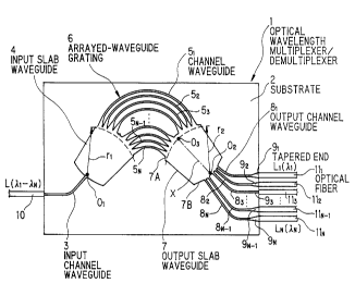
FIG. 4 shows the optical wavelength multiplexer/
demultiplexer in the preferred embodiment according to the
invention. The optical wavelength multiplexer/demultiplexer, which
is similar to the conventional one shown in FIG. 1, comprises an
input channel waveguide 3, an input slab waveguide 4, an arrayed-
CA 0221297~ 1997-08-13
- 1 0 -
waveguide grating 6 comprising N channel waveguides 51- 5N ~ an
output slab waveguide 7, and N output channel waveguides 81 - 8~
. In the embodiment, each output channel waveguide 81 - 8~ is
provided with an outwardly tapered end 9l - 9.~ at their output
ends. All these elements are incorporated in a substrate 2 and
preferably covered with a cladding layer 12, as shown in FIG. 5, to
form a single optical wavelength multiplexer/ demultiplexer 1.
FIG. 5 shows the vicinity of the output ends of the output
channel waveguides 8, - 8~ . According to the preferred
embodiment, each outwardly tapered end 9, - 9~ has a width W at its
end surface which becomes larger as the output channel waveguide
becomes more distant from the symmetrical axis X of the output slab
waveguide 7.
FIG. 6 shows a preferable connecting structure of the output
channel waveguide 8i (i=1- N) to an optical fiber lli(i=1- N) in
the preferred embodiment. The output channel waveguide 8i has the
outwardly tapered end 9i(i=1- N) through which the signal Li(i=1- N)
at wavelengthl i (i=1- N) is coupled to the optical fiber lli(i=1-
N). The optical fiber 11 comprises a core llA and a cladding layer
llB. The width W of the tapered end 9i at its end surface 8A is
designed in such a way that, for example, it becomes larger in a
range between 4 - 10 ~ m as the output channel waveguide 8i becomes
more distant from the symmetrical axis X of the output slab
waveguide 7, provided the specific refractive index difference
between the output channel waveguide 8i and the cladding layer 12 is
0.75 %.
FIG. 7 shows characteristics of coupling loss between the
output channel waveguide 8i and the optical fiber lli relative to
CA 0221297~ 1997-08-13
- 1 1 -
the width W of the tapered end 9i, wherein the output channel
waveguide 8i is 6 ~ m wide and 6 ~ m thick. A specific refractive
index difference between the output channel waveguide 8i and the
cladding layer 12 is 0. 75 %. The optical fiber lli has a mode field
diameter of 9.7~ m. As shown in FIG. 7, the coupling loss becomes
lower as the width of the tapered end becomes larger, then it
becomes minimum at the width of 10.0 u m. Therefore, according to
the preferred embodiment, the output channel waveguides are
designed in such a way that the coupling loss between the output
channel waveguide 8i and the optical fiber lli becomes lower, as the
output channel waveguide 8i becomes more distant from the
symmetrical axis X of the output slab waveguide 7. The coupling
loss, however, becomes higher when the width W is larger than 10~ m
(i.e., W > 10 ~ m).
In operation, the wavelength-division multiplexed signal L,
which is coupled into the input channel waveguide 4 through an
optical fiber 10, expands into the input slab waveguide 4 by
diffraction. Then, the expanded signals are distributed to the
channel waveguides 51 - 5~ of the arrayed-waveguide grating 6.
Since each channel waveguide 5,- 5N of the arrayed-waveguide 6 has
a predetermined waveguide length difference, each signal at
different wavelength, after traveling over each channel waveguide
5~ - 5~ , has a predetermined phase difference according to its
waveguide length difference. Since the phase difference depends on
the wavelength of the signal, each signal at different wavelength
is focused on a different position along the connecting boundary 7B
of the output slab waveguide 7 due to a lens effect. For example,
the signal at wavelength l 1 distributed into and emerging from the
CA 0221297~ 1997-08-13
channel waveguides 51 - 5N ~ is focused at the input end of the
output channel waveguide 81. In the same way, the signals at
wavelengths l 2 - A N are focused at the input ends of the output
channel waveguides 8, - 8N , respectively. As a result, separated
signals L1- L~ at different wavelength A 1 - A N are selectively
received by the output channel waveguides 81- 8~ and emerge from
their output ends through the tapered ends 91- 9~ to be coupled to
optical fibers ll1 - ll N ~ respectively.
Although each separated signal Li- L ~ coupled into each
output channel waveguide 81- 8N suffers a different loss from
other when it is separated from the multiplexed signals, i.e., the
loss becomes higher as the output channel waveguide becomes more
distant-from the symmetrical axis X of the output slab waveguide 7,
such loss differences may be reduced due to the different coupling
losses created by the varied widths W of the tapered ends 91- 9~
in accordance with the invention. Because the coupling loss becomes
lower as the output channel waveguide becomes more distant from the
symmetrical axis X of the output slab waveguide 7, the loss
differences may be adjusted to be substantially equal and the
separated signals L,- LN with reduced loss differences emerge from
the output channel waveguides 81- 8Y and are coupled into the
optical fibers ll~ , respectively.
Next, loss relative to wavelength characteristics in the
optical wavelength multiplexer/demultiplexer l in the preferred
embodiment will be discussed below, wherein eight channel
waveguides 81 - 89(N=8) emerge eight signals L1 - L8 at eight
wavelengths A 1 - A ~, respectively. Each output channel waveguide
81 - 8~ is 6 ~ m wide and 6 ~ m thick, and a specific refractive
CA 0221297~ 1997-08-13
- 1 3 -
index difference between each output channel waveguide 81- 83 and
the cladding layer 12 is 0.75 %. The optical fiber lli has a mode
field diameter of 9.7 ~ m.
In this case, the width W of the tapered end of each output
channel waveguide 8l - 88 is selected as shown in TABLE 1. For
example, the tapered ends 9~, 93 of the output channel waveguides
81, 88 which are more distant from the symmetrical axis X of the
output slab waveguide 7 are 10 ~ m wide at their end surfaces,
while the tapered ends 9ll 98 of the output channel waveguides 84~8s
which are closer to the symmetrical axis X of the output slab
waveguide 7 are 5~ m wide.
TABLE 1
OUTPUT CHANNEL WAVEGUIDE TAPERED END WIDTH(~ m)
81 10 . O
8z 9.0
83 7.0
84 5.0
8s 5.0
86 7.0
87 9.0
88 10.0
FIG. 8 shows loss relative to wavelength characteristics in
the optical wavelength multiplexer/demultiplexer 1 in the preferred
embodiment, wherein eight channel waveguides 81 - 88 (N=8) emerge
eight signals Ll - L8 at eight wavelengths l ~ - ~ 8, respectively.
As is indicated in FIG. 8, a loss difference between the signals
CA 0221297~ 1997-08-13
L, (~ ,), L5 (A s) from the output channel waveguides 8,, 8s which
are close to the symmetrical axis X, and the signals L~ L8 (
A ~) from the output channel waveguides 81t 88 which are distant
from the symmetrical axis X, is as low as 0.65 dB, which is
improved from 0.9 dB of the conventional one.
In the preferred embodiment, the substrate may be a glass
substrate, a semiconductor substrate or the like. The waveguides and
the cladding layer may be made of properly selected transparent
materials such as glass, semiconductor, or the like. For example,
the substrate may be made of SiO2, while the input channel
waveguide, the input slab waveguide, the arrayed-waveguide grating,
the output slab waveguide and the output channel waveguides are made
of TiO2-SiO2, and the cladding layer may be made of B2 03 -P20s-SiO2.
Moreover, if a buffer layer is formed between the substrate and the
waveguides, the substrate may be made of Si substrate, while the
buffer layer, the waveguide and cladding layer may be made of SiO2,
TiO2-SiO2, and B2 03 -P20s-SiO2~ respectively.
Besides selecting the width of each tapered end, the loss
differences may be reduced in other ways, for example, by properly
selecting a light coupling efficiency of each output channel
waveguide and an output optical fiber by positioning light coupling
means like a focusing lens between an end surface of each output
channel waveguide and an optical fiber.
Moreover, if a plurality of signals of different wavelengths
are combined at the optical wavelength multiplexer/demultiplexer
according to the invention, i.e., the signals are transmitted in the
opposite direction to those in the aforementioned preferred
embodiment, an input loss of each input channel waveguide (i.e.,
CA 0221297~ 1997-08-13
- 1 5 -
each output channel waveguide in the preferred embodiment) may be
properly selected in accordance with a different combining loss
suffered by each signal.
Although the invention has been described with respect to
specific embodiment for complete and clear disclosure, the appended
claims are not to be thus limited but are to be construed as
embodying all modification and alternative constructions that may
be occur to one skilled in the art which fairly fall within the
basic teaching here is set forth.