Note: Descriptions are shown in the official language in which they were submitted.
CA 02212999 1997-08-14
FILTER HAVING TUNABLE CENTER FREQUENCY
AND/OR TUNABLE BANDWIDTH
BACKGROUND
1. Field of the Invention
s The invention relates generally to RF filters, and more specifically to RF filters
with one or more adjustable characteristics.
2. Description of Related Art
State-of-the-art RF filters are eommonly implemented through the use of a
plurality of parallel-resonant LC sections that are capacitively coupled to the source, to the
0 load, and to each other. In many applications, it would be desirable to provide a
mechanism by which the center frequency and/or the bandwidth of such a filter may be
adjusted. To this end, various techniques have been used to provide filters having tunable
characteristics. In general, these techniques involve ch:~nging the reactance of one or
more filter components. For example, many low-cost portable A~I/FM radios use a
m~ch~nical multi-gang variable capacitor, in combination with fixed inductors, to provide
tuning across the AM and FM broadcast bands.
Electronically-tunable filter designs incorporate varactor diodes into the parallel-
resonant LC sections, and/or use varactor diodes to control the capacitive coupling
elements of the filter. Varactor diodes may be conceptualized as voltage-controlled
variable capaeitors, because the capacitance provided by a varactor diode is roughly
proportional to the reverse DC bias applied to the varactor diode. Varactor diodes have
been used to make RF filters having tunable center frequencies and/or tunable bandwidth.
In a typical filter arrangement providing for adjustment of center frequency, each
parallel-resonant LC section of the filter includes a tuning element comprising one or more
varactor diodes. The capacitance of the diodes is set to a desired value by adjusting a DC
CA 02212999 1997-08-14
control voltage, thereby "tuning" the RF filter to a desired center frequency. In a typical
filter arrangement providing for adjustment of bandwidth, one or more of the capacitive
coupling elements of the filter includes a varactor diode for adjusting the amount of
coupling between adjacent parallel-resonant sections of the filter, and/or for adjusting the
5 coupling between the filter and a sourceAoad element.
In many system applications, it would be desirable to minimi7ç the number of
varactor diodes that are used in an electronically-tunable filter while, at the same time,
providing a filter having adjustable bandwidth and adjustable center frequency. In order to
provide an electronically-tunable filter with these adjustable properties, prior art designs
10 require the use of a first set of varactor diodes to adjust the bandwidth, and another set of
varactor diodes to adjust the center frequency. Since varactor diodes add cost to a filter
design, it is desirable to keep the number of varactor diodes in a filter design to a
As the number of varactor diodes in a filter is increased, it becomes increasingly
5 difficult to propelly align the filter. Since two varactor diodes will generally not exhibit
identical voltage-versus-capacitance characteristics, tracking mechanisms are used to
compensate for inherent device-to-device variations, such that, for example, all resonant
elements will be tuned to the same frequency at a given varactor DC supply voltage.
These tracking mech~ni.~m~ typically take the form of variable trimrner capacitors and/or
20 variable resistors (potentiometers). As the number of varactor diodes in a filter is
increased, it becomes increasingly difficult and time-consuming to properly adjust filter
tracking. For these reasons, it would be desirable to ~ the number of varactor
diodes used in an adjustable filter design.
The capacitance provided by a varactor diode is linearly related to the applied
25 reverse bias voltage only over a certain range of reverse bias voltages. Outside of this
voltage range, the varactor diode exhibits nonlinear properties and provides a capacitance
with an insufficiently high Q (i.e., the capacitance is swamped by too much series
resistance). Even within the linear operating region of the varactor diode, the Q of a
CA 02212999 1997-08-14
varactor diode is often lower than that of a conventional air-dielectric or mica-dielectric
variable capacitor. If a filter design requires relatively high-Q elements, it may not be
possible to achieve a desired level of performance with varactor diodes. In a similar vein,
varactor diodes are more vulnerable to relatively high levels of applied RF energy than is
s the case with mechanical capacitors. When confronted with strong RF input signals,
varactor diodes can introduce intermodulation and other spurious products into a filtered
signal.
One technique for providing a tunable resonator element, while at the same time
overcoming the disadvantages of varactor diodes, is described in U.S. Patent No.0 5,065,121 issued to Masood Ghadaksaz on November 12, 1991 (hereinafter, Ghadaksa_).
Gh~d:~k.~37. discloses a single resonator element that has a selectable center frequency.
The center frequency is changed by electronically switching a plurality of fixed inductive
and capacitive elements into a resonant circuit. However, Gh~ c~7 does not describe any
mechanism for tuning the bandwidth of the resonator element, nor does Gh~d~7 describe
how a plurality of resonator elements could be combined with other reactive elements to
form an RF filter. Therefore, there is a need for a tunable filter design which minimi7Ps
the number of tunable filter elements while providing a mech:~nicm for adjusting center
frequency and bandwidth.
SUMMARY OF THE INVENTION
In an RF filter having an input terminal, an output terminal, a plurality of resonator
elements, and a plurality of coupling reactances for coupling one resonator element to
another resonator element, for coupling the input terminal to a resonator element, and for
coupling the output terminal to a resonator element, techniques are disclosed for providing
an RF filter having an electronically tunable center frequency and/or an electronically
tunable bandwidth. According to a specific embodiment disclosed herein, a first shunt
reactance is provided from the input terminal to ground, and a second shunt reactance is
provided from the output terminal to ground. The values of the coupling reactances
remain constant, while the values of the resonator elements, the first shunt reactance, and
CA 02212999 1997-08-14
the second shunt reactance are tuned to provide a specified filter bandwidth and/or a
specified center frequency.
BRIEF DESCRIPTION OF THE DRAWINGS
FIG. I is a schematic diagram of a prior-art capacitively-coupled, multi-resonator
RF bandpass filter.
FIG. 2 is a schematic diagram of a capacitively-coupled, multi-resonator RF
bandpass filter constructed according to a first illustrative embodiment of the present
nvention.
FIG. 3 is a schematic diagram of the bandpass filter of FIG. 2 redrawn for
0 purposes of mathematical analysis.
FIG. 4 is a schematic diagram showing an illustrative technique for determining
filter input and/or output impedances.
DETAILED DESCRIPTION OF THE PREFERRED EMBODIMENTS
FIG. 1 is a schematic diagram of a prior-art capacitively-coupled, multi-resonator
RF bandpass filter. The filter includes a first coupling capacitor 101 for coupling the filter
to a source, a second coupling capacitor 107 for coupling the filter to a load, a first
impedance transforming capacitor 109 for matching the impedance of the filter to the
impedance of the source, and a second impedance transforming capacitor 117 for
matching the impedance of the filter to the impedance of the load. A first resonator
20 element includes capacitor 111 and inductor 119 connected in parallel, a second resonator
element includes capacitor 113 and inductor 121 connected in parallel, and a third
resonator element includes capacitor 115 and inductor 123 connected in parallel. A third
coupling capacitor 103 couples the first resonator element to the second resonator
CA 02212999 1997-08-14
element, and a fourth coupling capacitor 105 couples the second resonator element to the
third resonator element.
Capacitors 101, 103, 105, 107, 109, 1 1 1, 113, 1 15, and 117 are shown as variable
capacitors for purposes of illustration, to demonstrate that the values of these capacitors
s may have to be changed if it is desired to change the bandwidth and/or the center
frequency of the filter. The values of these capacitors must be adjusted if it is desired to
maintain the same filter shape factor at each of a plurality of center frequencies and/or
filter bandwidths. After appropriate values for these capacitors are determined, any
desired combination of fixed-value capacitors, equivalent transmission line sections, and/or
0 trimmer capacitors may actually, in fact, be employed to implement the filter of FIG. 1.
Adapting the filter design of FIG. 1 for use at a plurality of center frequencies
and/or bandwidths, while providing a substantially constant filter shape factor, requires a
determination of capacitance values for capacitors 101, 103, 105, 107, 109, 111, 113,
115, and 117. Unfortunately, in many real-world applications, it is desirable to minimi7~,
the number of capacitance values that must be changed when adapting a filter to a new
desired bandwidth and/or a new desired center frequency.
Assume, for example, that it is desired to change the bandwidth of a given filter
design. In order to improve upon the prior art approach, further assume that a constraint
is placed on the values of the series coupling capacitors -- namely, capacitors 103 and 105
20 -- specifying that the values of these capacitors are to remain constant, irrespective of the
filter center frequency and the filter bandwidth. In this manner, the number of capacitance
values that must be changed is reduced. However, for these series coupling capacitors,
capacitors 103 and 105, to remain constant for any center frequency or bandwidthselected, it then becomes necessary to rely upon changes in the capacitances of resonator
2s capacitors 111, 113, and 115 and, additionally, changes in the inductances of resonator
inductors I 19, 121, and 123, in order to provide a desired filter frequency response. Since
the capacitances of the resonator capacitors 111, 113, 115 and the inductances of the
resonator inductors I 19, 121,123 are mathematically related to the filter center frequency
CA 02212999 1997-08-14
and the filter bandwidth, it is conceivable that an adjustable-bandwidth and adjustable
center frequency filter could be developed that uses fixed values for the coupling
capacitors, even though such an approach has not been adopted in the prior art.
Upon further consideration, it becomes apparent that the circuit configuration of
s FIG. I cannot yield a practical filter having a tunable bandwidth as well as a tunable center
frequency if the values of the coupling capacitors 103, 105 are held constant. Using any
of a variety of mathematical filter analysis tools well-known to those skilled in the art, it is
soon discovered that such a filter has a shape factor that varies rather significantly from
one filter center frequency to another, rendering the filter unsuitable for many real-world
o applications such as cellular telephony. For example, a cellular telephone filter designed to
have an adjustable center frequency in the range of 860-890 Mhz would exhibit
substantially different performance at a center frequency of 860 Mhz than at a center
frequency of 890 Mhz. The differences in performance at different center frequencies
could involve changes in skirt selectivity, harmonic rejection, and/or other filter
parameters. Ideally, when the center frequency of the filter is changed from 860 Mhz to
890 Mhz, only the center frequency of the filter should change, and all other filter
parameters should remain substantially the same.
The circuit configuration of FIG. 1 cannot provide a filter having a characteristic
that, when the center frequency is changed, all other filter parameters remain substantially
20 the same, if the values of coupling capacitors 103, 105 are held constant. In order to keep
the values of coupling capacitors 103, 105 fixed whilst, at the same time, changing the
bandwidth and/or the center frequency of the filter, but not significantly changing the
shape factor of the filter, the circuit configuration of FIG. 1 is entirely unsuitable.
FIG. 2 is a schematic diagram showing an adjustable-bandwidth, adjustable center25 frequency filter constructed in accordance with a preferred embodiment disclosed herein.
The filter configuration of FIG. 2 provides a tunable bandwidth as well as a tunable center
frequency, even if the values of the coupling capacitors 103, 105 are held constant. In
order to keep the values of coupling capacitors 103, 105 fixed whilst, at the same time,
CA 02212999 1997-08-14
ch;~nging the bandwidth and/or the center frequency of the filter, the circuit configuration
of FIG. 2 includes various novel features to be described below.
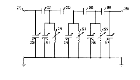
Referring now to FIG. 2, a first shunt capacitor 209 is provided that is in shunt
between filter input terrninal 270 and ground, and a second shunt capacitor 217 is
s provided that is in shunt between filter output terminal 280 and ground. A first series
coupling capacitor 201 couples the filter input terminal 270 to filter resonator elements to
be described below, and a second series coupling capacitor 207 couples the filter output
terminal 280 to filter resonator elements to be described below. These first and second
shunt capacitors 209, 217 must be placed at the filter input and output terminals,
0 respectively, to m~int~in a substantially constant coupling impedance to filter sources
and/or filter loads across a given frequency range. To this end, note that shunt capacitor
209 forms a capacitive divider with series coupling capacitor 201, and that shunt capacitor
217 forms a capacitive divider with series coupling capacitor 207.
Series coupling capacitor 201 couples the filter input terminal 270 to a first
resonator element comprising a first resonator capacitor 211 and a first resonator inductor
221. Although, in the example of FIG. 2, discrete inductors and capacitors are used to
implement the resonator elements, this is shown for purposes of illustration. Resonator
elements could also be implemented using appropriate sections of transmission lines, for
example. In such a case, a desired amount of inductance or capacitance is provided by
20 adjusting the length of a transmission line section to an app,op,iate value. The first
resonator element is coupled, through series coupling capacitor 203, to a second resonator
element that includes second resonator capacitor 213 and second resonator inductor 223.
The second resonator element is coupled, through series coupling capacitor 205, to a third
resonator element that includes third resonator capacitor 215 and third resonator inductor
25 225. The third resonator element is coupled to the filter output terrninal 280 through
series coupling capacitor 207.
Note that, in the configuration of FIG. 2, capacitors 201, 203, 205, 207, 209, and
217 are shown as fixed capacitors, whereas capacitors 211, 213, and 215 are shown as
CA 02212999 1997-08-14
variable capacitors. This does not imply that, in practice, the capacitors in question should
be implemented with actual variable or fixed capacitors. Rather, as employed in FIG. 2,
the variable capacitor symbol is used to indicate that the capacitances of these capacitors
are changed in order to tune the filter from a first center frequency to a second center
5 frequency, and/or to tune the filter from a first bandwidth to a second bandwidth. The
fixed capacitor symbols are used to indicate that the capacitances of these capacitors are
to remain constant when the filter is tuned from a first center frequency to a second center
frequency, and/or tuned from a first bandwidth to a second bandwidth.
Although the schematic diagram of FIG. 2 shows discrete (lumped) capacitor and
10 inductor elements, this is for purposes of illustration, as one or more of these discrete
(lumped) elements could be replaced with a distributed element, such as a transmission
line section of an appropriate impedance to provide the required inductive and/or
capacitive reactance. At a given frequency, shorted transmission lines that are somewhat
less than one quarter wavelength long provide inductive reactance, hence acting as an
5 inductor. Shorted transmission lines somewhat more than a quarter wavelength long
provide capacitive reactance, hence acting as a capacitor.
One technique for changing the values of inductive and/or capacitive reactance in
the resonator elements of FIG. 2 is to switch any of a plurality of capacitive and/or
inductive reactances into and/or out of the resonator element. For example, FETs may be
20 used as RF switches in series with an inductive or capacitive element, thereby switching
inductance and/or capacitance into and/or out of a given resonator element to achieve the
desired changes in resonator element reactances.
FIG. 3 is a schematic diagram of the bandpass filter of FIG. 2 redrawn for
purposes of mathematical analysis. The circuit configuration of FIG. 3 includes a first
25 shunt capacitor, CS0, in shunt with the filter input, a second shunt capacitor, CL0, irl
shunt with the filter output, a third shunt capacitance ClS in parallel with a first shunt
inductance Ll, a fourth shunt capacitance C2S in parallel with a second shunt inductance
CA 02212999 1997-08-14
L2, a fifth shunt capacitance C3S in parallel with a third shunt inductance L3, and four
series coupling capacitors CSl, C12, C23, and C3L. For analytical purposes, two shunt
capacitors, each having negative capacitance, are postulated, shown as - CIM and - COM.
In practice, discrete negative capacitance elements need not be employed to implement
5 ClM and - COM, as the values of - ClM and - COM are absorbed into the values of L1
and/or ClS in the case of - ClM, and L3 and/or C3S in the case of - COM, as was
previously shown in FIG. 2.
The circuit configuration of FIG. 3 may be mathematically analyzed to show that
the circuit provides a filter having adjustable bandwidth and/or center frequency, while all
o other filter parameters remain substantially constant. For purposes of the analysis, the
following definitions apply:
k; k - the ratio of the resonant frequency of the ith and kth resonator elements to
the 3dB cutoff frequency in the low-pass equivalent circuit.
qj - the quality factor of the ith resonator element, influenced by the source or load
resistance, if present in parallel or in series.
~f - the 3dB bandwidth of the filter in Hertz (Hz)
frn - the center frequency of the filter in Hz.
QO - the quality factor of the resonator.
The following equations are used to analyze the filter of FIG. 3. Note that the
20 variables used in these equations were defined in the immediately preceding paragraph.
( I ) Kj k= ki~k*~flfm
CA 02212999 1997-08-14
(2) Qi = qi*f,./~f
(3) Ci k = Kj k*(C~*C,I)l'2, where C, is the total nodal capacitance at a circuit
node i. Note that all nodes other than node i are conceptualized as being
grounded for purposes of this equation, and that C~l is the total nodal
capacitance at node k.
(4) fm = I/[2*1l*(Lj*CI)"2], where Lj is the total nodal inductance at node i.
For the configuration of FIG. 2 where capacitive coupling is used, then L
represents the inductance of the inductor in a respective resonator element.
(S) Z5~c = jZ*tan(,~*I) = jZO*tan(2*~1*1/~), for a shorted transmission line, where 1/~ is the length of the resonator in wavelengths. Note for
1/~ < l/4, the resonator is inductive, and for l/~ > l/4, the resonator is
capacitive.
(6) Zk = jZo*COt(,~*I) = jZ*Cot(2*~*1/~), for an open transmission line,
where l/~ is the length of the resonator in wavelengths. Note for
l/~< l/4, the resonator is capacitive, and for l/~ l/4, the resonator is
inductive.
(7) Cl=ClS+Cl2=~ClS=CI-Cl2
(8) Cll= C2S + C12 + C23 ~ C2S = Cn- Cl2 - C23
(9) Cm = C3S + C23 =, C3S = Cm - C23
Since capacitive coupling is used, and all resonant elements, i.e., all nodes,
resonate at the same frequency, it follows that:
CA 02212999 1997-08-14
(10) Cl=Cn=Cm=C
(11) Ll =L2=L3=L
( 12) qO = ~f/fm QO
(13) C12 = kl2*~f/fm*(C,*Cn)"2 = k,2*~f/fm*C
(14) C23 = k23*~f/fm*(CII*CII)l/2 = k23*~f/fm*C
For C12 and C23 to remain constant for ~f and for fm movement, the nodal
capacitance, C, must change; therefore, the nodal inductance must also change. Note that
for a chosen filter topology kik does not change; for kjk to change either the filter
topology must change (i.e. Butterworth to 0.1 dB ripple Chebyshev) or the number of
0 poles (elements) must change.
( 15) C - f(fm, ~f) = ~* fm/~f, where f(fm, ~f) is a function of fm, ~f and ~ is an
arbitrary constant.
Using equations (7) and (15),
(16) ClS = C - kl 2*~f/fm*C = C*[(fm- kl 2*~f)/fm] = ~* fm/~f*[(fm- kl 2*~f)/fm]
(17) ClS = Y*(fm/~f - k, 2)
Similarly, for C2S and C3S,
( 18) C2S = y* (fm/~f - k, 2 - k2.3)
CA 02212999 1997-08-14
( 19) C3S = ~/* (fm/~f - k2 3)
Equations (17) ~ (19) place boundaries on realizable values of ClS ~ C3S,
(20) f~ f 2 k~ 2 + k2 3
Practically, fm/~f must be greater than the value given in (22), because of parasitic
5 capacitances and manufacturability reasons.
From equations (4) and ( 15),
(21) I/(L*C) = (2*~)2 *(fm)2
(22) L = l/[C* (2*~)2 *(fm)2] = l/[y* (fm/Qf* (2*lt)2 *(fm)2]
(23) L - ~f /[~* (2*Jc)2 *(fm)3]
o Equations (14), (17) ~ (19), and (23) provide some insight into the required
"metamorphosis" in the resonator.
A) The total nodal capacitance is a linear function of the center frequency (fm) and
is a linear function of l/~f (~f is the 3dB bandwidth) as required by the
stipulation to keep the series capacitors constant with ~f and fm.
]5 B) The total nodal inductance (same as the resonator inductance in this case) is a
linear function of the 3dB bandwidth (~f) and a cubic function of l/fm.
C) The resonator capacitance is a linear function of fm and l/~f, just as the nodal
capacitance, only a constant ~ * ~ (kj k) separates the two.
CA 02212999 1997-08-14
If the "L" and "C" in the resonator are to be realized with open or shorted
transmission lines, the lengths of those lines for various center frequencies
and bandwidths must be determined. Using equations (5), (6), (17)
(19), and (23);
s (24) ~, *L = ZO *tan (2*tl1 lt~), for a shorted line of length, O < I l < ~4, or
an open line of length, ~/4 < ( I I + ~/4) < ~12.
(25) ~m*C = (l/Zo)* tan(2*~ ), for an open line of length, O < I 1 < ~J4, or
a shorted line of length, ~/4 < ( I 1 + ~4) < ~2.
To verify the foregoing mathematical analysis, three different filter topologies were
0 simulated using a software package well-known to those skilled in the art as the
EaglewareTM RF linear simulator. The center frequencies bandwidths, required nodal
capacitances and inductances, given in Table I below, can be obtained from the equations
presented above.
-
CA 02212999 1997-08-14
14
Table 1: Center Frequencies, Bandwidths, Nodal Capacitances
and Inductances for RF Simulations
fm(MHz) 838 1880 2~
~f(MHZ) 25 60 84
f,~ f 33.52 31.33 29.10
C (pF) 5.03 4.70 4.36
L (nH) 7.17 1.52 0-97
For the filter to be tunable and for the coupling capacitors to be constant, thefollowing considerations apply. The two coupling capacitors CS 1, C3L of FIG. 3 provide
5 a reactance that changes with frequency, thereby causing load and source coupling to the
filter to vary with frequency. To keep load and source coupling to the filter at a relatively
constant level as the center frequency and/or bandwidth are changed or "tuned", a
capacitor CS0 from the input node (input terminal) to ground is incorporated into the
design of FIG. 3. Another capacitor CL0 is used from the output node (output terminals)
o ~o ground. These shunt capacitors CS0 and CL0 allow the coupling capacitors CS 1, C 12,
C23, and C3L to remain constant, while the capacitances of capacitors CS0, ClS, C2S,
C3S, and CL0 must be adjusted as the center frequency and bandwidth is changed or
"tuned". Refer to FIG. 4, to be described below for further mathematical derivations.
Some points to note:
CA 02212999 1997-08-14
~ all of the series capacitors, namely, capacitors CS1, C12, C23 and C3L remain
at the same value for the three different center frequencies and bandwidths set
forth in TABLE 1 (within roundoff error.)
~ both the shunt C's and the shunt L's, namely, capacitors CS0, ClS, C2S, C3S
and CL0, and inductors L1, L2, and L3 must change in value for the different
center frequencies and bandwidths, with the L's having to change over a 7.0: 1
ratio and the C's changing by a ratio of less than 1.9: 1.
~ the filters are able to maintain the same shape or filter type as they are "tuned".
Practical Implementation
0 An implementation of the filter in FIG. 2 will use some type of mechanism for
tuning the shunt L's (inductors 221, 223, 225) and the shunt C's (capacitors 209, 211,
213, 215, 217). Although any of several techniques well-known to those skilled in the art
could be employed for this purpose (i.e., varactor diodes, etc), one illustrative approach
uses tunable transmission line sections to implement one or more of the shunt C's and/or
shunt L's. As discussed previously, shorted transmission line sections less than one
quarter wavelength at the center frequency provide inductive reactance, whereas shorted
transmission line sections greater than one quarter wavelength at the center frequency
provide capacitive reactance. RF switches from the center conductor (i.e., the hot
conductor and/or the conductor that is not at RF ground potential) of a respective
20 transmission line section to ground, such as FET switches, may be provided at several
appropriate locations along a given transmission line. These FETs are switched on and/or
off, thereby changing the capacitance and inductance of the shunt elements, and changing
the center frequency and/or bandwidth of the filter to a desired value.
With reference to FIG. 4, it is desired that the input impedance, Zin~ be equal to
25 R2. Mathematically, set
CA 02212999 1997-08-14
16
Zin=(l + jo*Rl*CI + jc~*Rl*C2) /
*C2 + j~*C3 - c~2*Rl*Cl*C2 - c1)2*Rl*Cl*C3 - ~2*RI*C2*C3) = R2
(Equation A I )
The im~gin~ry term of Equation Al must equal zero; therefore,
*RI*CI + cl)*Rl*C2 = cl)*R2*C2 + ~*R2*C3 (Equation A2)
Again, it is desired that the coupling capacitor be constant regardless of the Rl and R2
value; this (R1 -> R2) is the impedance transforrnation that occurs by varying only the
shunt values of capacitance, when the center frequency or the bandwith changes. Using
this fact and rewriting Equation A2,
lo C2 = k = (-Rl*C1 + R2*C3) / (Rl - R2) (Equation A3)
Rewriting Equation A3,
Cl= (R2/RI)*[C3 - k* (Rl/R2 - 1)] (Equation A4)
Using Equation A4 and setting the real terms of Equation Al to R2 provides,
I = c~)2*Rl*R2*(Cl*C2 + Cl*C3 + C2*C3) (Equation A5)
Substituting, C2 = k and Equation A4 into Equation AS and manipulating the termsprovides,
I = c1)2*R22*[k*C3 - k2*(RI/R2 - 1) + C32 k*C3*(RI/R2 - 1) + k*RI/R2*C3]
(Equation A6)
CA 02212999 1997-08-14
Rewriting Equation A6 provides,
C32 + C3*2*k + [1/(~2*R22) - k2*(RI/R2 - 1)] = O (Equation A7)
Taking only the positive root to Equation A7 provides,
C3 = k* { [(~2*k2*R 1 *R2 - 1 ) "21 (~*R2*k)] - 1 ~ (Equation A8)
S From Equations A8, A4 and A3, the capacitive transformer equations are solved.
Note: For C3 > O, from Equation A8,
~ 2*k2*Rl *R2 - 1) = ~2*R22*k2 (Equation A9)
Rewriting Equation A9 gives,
Rl > [(~2*k2*R22 + 1) / ( cl)2*k2*R2)] > R2 (Equation A10)
o With C2 chosen greater than zero and using Equation A10,
-Rl*C1 + R2*C3 > O (Equation A11)
Rewriting Equation A 1 1,
C 1 < (R2/R I )*C3 (Equation A 12)