Note: Descriptions are shown in the official language in which they were submitted.
CA 02213259 1997-08-18
W O 97/23863 PCT/GB96/03077
I
MULTIPLEX ADDRES~ING OF FERROELECTRIC LIQUID CRYSTAL
DISPLAYS
5 This invention relates to the multiplex addressing of ferroelectric liquid crystal (FELC)
displays.
Such displays typically comprise a layer of a FELC material contained between two
cell walls each carrying strip electrodes forrning an x, y matrix of addressable10 elements or pixels, at electrode intersections.
One type of device is known as a surface stabilised FELC display; see for example
Meyer~ R B 1977 Molec. Crystals liq. Crystals 40, 33, and Clark, N A ,and
Lagerwall, S T, 1980, Appl. Phys. Lett. 36, 899. It can be switched between two
15 molecular orientations by a dc pulse of suitable amplitude, time, and sign.
Conceptually the liquid crystal molecules can be considered as rotating around aconical surface as the m~teri~l iS switched.
One prior art addressing scheme uses a strobe pulse of duration two time slots (ts). and
~20 amplitude zero in the first time slot, Vs in the second time slot sequentially applied to
each x row electrode in turn. l\~e~ntime one of two data waveforms are applied to each
y colurnn electrode. The data waveforms are alternative dc pulses of a]lternate polarity
and equal magnitude (+Vd, -Vd) each pulse lasting lts; one data waveforrn is theinverse of the other. This is termed a mono pulse strobe addressing scheme.
CA 02213259 1997-08-18
W O 97/23863 PCT/GB96/03077
Another addressing scheme; described in GB 2,232,802, uses a strobe waveforrn
having two pulses each lasting lts in combination with data waveforms as in the mono
pulse strobe scheme. The leading strobe pulse may be zero or non zero and of variable
5 amplitude and sign. Combination of strobe and data (resultant waveforrn) provides
two ~lirre,ent shapes of resultant.. This is useful in ch~ngin~: the switching
characteristics of the li~uid crystal material. The time taken to address each pixel in a
row is the line address time (lat) and for the above scheme is 2ts.
10 A variation of the above is described in GB 2,262,831. In this the strobe is applied to
each row in turn with a 2ts interval between applications of strobes to each new row,
as in the previous scheme. Additionally the strobe waveform is extended into theaddressing time of the next addressed row, ie for part of the time strobe waveforms are
being applied to 2 rows at the same time.
Another addressing scheme uses 4ts to address each pixel in a time. The strobe is a
zero for lts, then Vs for 3ts. Data waveforms are of arnplitude -Vd, +Vd, ~Vd, -Vd (or
the inverse) in successive time slots.
20 All addressing schemes must switch the material when required the difference
between srh~mesi5 their perf~ re Perforrnance is defined with respect to voltageused (low is desired), speed o~ switching (fast is desired), operating range (wide
difference between selected and non selected voltages), and low dep~n~lenre on pixel
pattern. A high contrast between the two switched states is also advantageous; as is a
25 wide operating range in Lell~pc;ldLule.
CA 02213259 1997-08-18
W O 97J23863 PCT/GB96/03077 --3--
As noted above molecules switch from one side to the other side of a. cone (eg ideally
switch between + 22~ to an alignment direction), due to the application of a dc voltage
applying a switching torque on each molecule. This switching torque causes switching
5 around the (im~in~ry) surface of a cone.
Previous addressing schemes have been empirical in nature, their desi.gn being based
on the results of experimental observation. Consequently the prior art addressing
scl~ , and in particular the pulse shapes, have not been opt;mi.~el1
This invention describes how the pulse shapes may be ~ n~A to improve switching
by considering the shape of applied field as the material is switching.
The present invention improves switching performance by m~ximi.~in~ the switching
15 torque applied to a molecule as it rotates around the cone surface; thi s is achieved by
varying the resultant voltage during the switching.
CA 022132~9 1997-08-18
W O 97/23863 PCT/GB96/03077
--4-
According to this invention a method of multiplex addressing a ferroelectric liquid
crystal display is as detailed in claim 1.
5 According to the invention the two data waveforrns have multiple levels (not just +t-
Vd), preferably dc balance, equivalent rms. Ievels but not necess~rily same shapes.
The strobe pulse is preferably the same when used with both select and nonselect data
waveforms, but may have multiple voltage levels.
10 According to this invention a multiplex addressed ferroelectric liquid crystal display
comprises a laver of chiral smectic liquid crystal material contained between two cell
walls, both surface treated to align the liquid crystal material~ a first series of spaced
strip (row) electrodes on one wall and a second series of spaced (colurnn) stripelectrodes on the other wall arranged to provide a matrix of addressable elements
15 (pixels), driver circuits for applying a strobe waveform to the first set of electrodes in a
sequence, and for applying one of two data waveforrns (select and non-select) to the
electrodes in the second set of electrodes characterised by:
means for generating a select and non-select data waveform having more than two
voltage levels (which may include a zero level), the two data waveforms having dc
20 balance and equivalent rms. values.
means for generating a strobe waveform,
the two data, and the strobe waveform CO-OI,~.d~ g to provide resultant values that
vary during the line address time to improve switching torque on material molecules
being switched and reduce switching torque on molecules not being switched.
2~
The data waveform may have at least 3ts and preferably more than 4ts. eg Sts, 6ts, 7ts,
8ts or more
CA 02213259 1997-08-18
W O 97/23863 PCT/GB96/03077
_ 5
The strobe waveforrn may be of two or more levels which may include a zero level.
The first pulse in the strobe waveform may be varied in amplitude and sign to vary
material ~wi~cl~ing characteristics and the waveform may extend in time into the line
5 addressing time of anofher row, as in GB-2,262,83 1.
The display m~tt-ri~l may be addressed in two fields, with reversal of strobe polarity
in 5llt(~ tf~ fields, m~king up a frame where fhe whole display is addressed to its
recluired pattern. ~lt~rn~ively the display may be blanked and then selectively
10 switched by one strobe waveforrn, polarity of hl~nkinp and strobe may he inverted
periodically to m~intslin dc balance. Blanking involves application of one or more
pulses of sufficient arnplitude-time product to cause a switching irrespective of what
data waveforrn is applied to column electrodes. The blanking may be on one or more
lines at a time in any desired sequence. The blanking pulse may be l)C b~l~nce~l with
1~ the strobe or may have extra portions to provide DC balance.
The m.qteri~l used in the device is one in which the value of the ratio of spontaneous
polarisation ~Ps) and dielectric biaxiality ( ~ ~ ) is preferably less than 0.01 Cm~2, for
example than 0.001 Cm-2.
The invention will now be described; by way of exarnple only, with reference to the
acco~ yh~g ~Ldwillgs of which:-
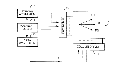
Figure 1 is a ~ mm~ti~ view of a x, y display with row and column drivers.
Figure 2 is a cross section of the display cell of Fig 1.
25 Figure 3 is a sr.hem~tic view of a layer of ferro electric liquid crystal material showing
one of a number of possible sllignment configurations.
Figure 4 is a sr.h~m~tic view showing one of the two allowable bistable positions of an
LC molecule and its envelope of movement around the imzlgin~ry surface of a cone.
Figure 5 is an end view of Fig 4 indicating several positions of a liquid crystal
30 molecule during switching.
-
CA 02213259 1997-08-18
WO 97123863 PCT/GB96/03077
- 6 -
Figures 6a~ 6b show ferroelectric and dielectric torque respectively against positions of
the li~uid crystal molecules in Fig 5.
Figures 7a, 7b shows switching torque and voltage against director position around a
switching cone.
5 Figure 8 shows an exarnple of resultant waveforrn suitable for switching the mzlt~
in Fig 5.
Fig 9 shows a resultant waveform, for use with waveforrn of Fig 8, which does not
cause switching.
Figure 10~ is a graph showing switching characteristics for one m~t-o:ri~l with the two
l O different addressing schemes shown in Figs 11 and 12.
Figure 11 shows a strobe, two data, and two resultant waveforms of a prior art
addressing scheme,.
Figures 12, 12a show strobe, data, and resultant waveform for two 4-slot sch~mes of
the present invention.
15 Figures 13-16 show s~,vitching char~ctPristics for dirr~lcllt shapes of a 4-slot scheme.
Figure 17 shows strobe, data, and res--lt~nt waveform for a 3-slot scheme.
Figure 18 shows strobe, data, and reslllt~nt waveforms for a 6-slot scheme.
Figure 19 shows strobe, data, and resultant waveforms for a 8-slot scheme.
Figure 20 shows switching characteristics for a 3-slot scheme of Fig 17.
20 Figures 21-2 2 show switching characteristics for non-select and select resultant
waveforms for the 8-slot scheme of Fig 19.
Figure 23 shows line address time against VstV for a prior art addressing scheme for
dir~c;ll~ pixel p~ of display.
Figure 24 shows lines address time against Vs/V for a three slot addressing scheme of
2~ this invention for dir~e~,L pixel patterns of disp}ay.
Figure 2~ shows switching characteristic for a device addressed by a scheme as in
Figure 11.
Figure 2~ shows switching characteristics for a device addressed by the present
invention~ the effects of diL~lent pixel patterns on switching points.
CA 02213259 1997-08-18
W O 97/23863 PCT/GB96/03077 -7-
The display 1 shown in Figures 1, 2 comprises two glass walls 2, 3 spaced about
1-6 lum apart by a spacer ring 4 and/or distributed spacers. Electrode structures 5, 6 of
tr~n~p~rent tin oxide are formed on the inner face of both walls. These electrodes are
5 shown as row and column forming an X, Y matrix but may be of other forms. For
example, radial and curved shape for an r, ~3 display, or of segment~ form for a digital
seven bar display.
A layer 7 of liquid crystal material is contained between the walls 2, 3 and spacer ring
10 4. Polarisers 8, 9 are arranged in front of and behind the cell 1. Row 10 and column
11 drivers apply voltage signals to the cell. Two sets of waveforms are generated for
supplying the row and column drivers 10, 11. A strobe waveform generator 12
supplies row wavefor~ns, and a date w~vt;rolln generator 13 supplies ON and OFF
waveforms to the column drivers 11. Overall control of timing and display format is
15 controlled by a contrast logic unit 14.
Prior to assembly the walls 2, 3 are surface treated eg by spinning on a thin layer of
polyam~de or polyimide, drying and where a~ro~liate curing, then buffing with a soft
cloth (eg rayon) in a single direction Rl, R2. This kno~,vn treatment provides a surface
2V ~ nment for liquid crystal molecules. In the absence of an applied electric field the
molecules tend to align themselves along the rubbing direction R~, R, and at an angle
of about 2~ to the surface. The rubbing directions Rl, R~ are paral}el in the same
direction as shown or may be ~ lel for some types of devices. When suitable
lmidirectiorl~l voltages are applied the molecular director aligns along~ one of two
2~ directions Dl D2 depending on polarity of the vol~age. Ideally the angle between Dl,
D2 is about 4~~, but varies with m~ttor~
CA 02213259 1997-08-18
WO 97/23863 PCT/GB96/03077 -8-
The device may operate in a tr~n.cmi~.cive or reflective mode. In the former light
passing throu~;h the device eg from a tlmg~ten bulb 15 is selectively tr~m~mitte(l or
blocked to form the desired display. In the reflective mode a mirror 16 is placed
S behind the second polariser 9 to reflect ambient light back through the cell 1 and two
polarisers 8, 9. By making the mirror 16 partly reflecting the device may be operated
both in a tr~n~mi.c.cive and reflective mode.
Figure 3 shows diagrammatically one arrangement of liquid crystal molecules 21 in a
10 layer. Molecules (more correctly the director) tend to lie as if on the surface of a cone
2 7, seen more clearly at Figure 4. A~ nt to the cell walls 2, 3 strong ~ligning forces
anchor the molecules in a tilted and aligned direction, away from the walls the
molecules tend to arrange themselves as shown in one of two stable positions 21, 21 '.
When a dc electric field of ~l,plo~,liate polarity is applied there is a coupling between
1~ the molecule and the field and the molecules rotate around the cone 22 from one
switched position 21 (shown in solid lines) to the other switched position 21 ' ~shown
in broken lines).
The present invention improves switching by aiming to maximise torque to the
20 molecules during switching by varying the ~mplit~ e of applied field during
switching.
2~
CA 02213259 1997-08-18
W O 97/23863 PCT/G B96/03077
_9
Figures S, 6a. 6b, show how torque varies as a molecule moves from ~ac (positionunder ac stabilised voltage) through A, B to ~s, which is halfway between its two
switched states, (thereafter it continues to move to its other switched position ~ac').
There are two different torques acting on the director, the ferroelectric torque and the
5 dielectric torque. The ferroelectric torque, Figure 6a, is the force proportional to
applied voltage acting on the director m~king it rotate round the cone surface 22. The
dielectric torque, Figure 6b is a torque tending to resist movement of the director and
is proportional to V2. To improve molecule switching, the voltage applied to thematerial is arranged so that the switching torque (difference between ferroelectric and
10 dielectric torque) is m~ximi.eeA as the director switches from ~ac, through A, B and ~s
for pixels nf~e~lin~ to be switched. For pixels required not to switch, then the switching
torque is minimieefl
As seen in Figure 7a, prior to switching the director has an angle of say 50~ from zero.
15 Application of a relatively small voltage of 1 Ov results in a small positive switching
torque, and the director starts to move. At around 74~ the voltage can. be increased to
20v, then at about 82~ and more the voltage increased to 30v, 40v etc up to 60v as
indicated by the Figure 7a. In contrast if the initially applied voltage is large, eg SOv
then the switching torque would be large and negative because the dielectric torque
20 predomin~te~ over the ferroelectric torque thereby slowing down switching.
2~
CA 02213259 1997-08-18
W O 97123863 PCT/GB96/03077
- 10-
An explanation of how the present invention improves the performance of
multiplexed devices follows particularly with reference to Figures 5, 6a and 6b..
Figure 5 illustrates the plan view of the cone of possible orientations for the director.
The liquid crystal moves about this cone through changes in the orientation angle
5 only in response to the applied electric field. The actual device configuration from one
surface to the other is complicated, depending on the alignment and applied electric
field. For simplicity, a ul~irollll structure is ~.sllm~ in which the director is at some
orientation ~ throughout the sample. Switching occurs when the electric field results in
a net torque on the molecules tentling to change ~. How rapid the switching is
10 depends on the magnitude of the tor~ue and the total change in orie~tation through
which the molecules move. Ferroelectric liquid crystal devices switch as a result of a
r~et DC field favouring one side of the cone (either left or right in Figure 5). The
starting orientation is ~ac (resulting from the AC field effect usually from the data
waveform~ and ~wil~;hillg occurs when a net DC of the correct polarity tends to cause
15 reorientation towards ~s (once the director has passed ~s the pixel will have latched
and will relax to the other side of the cone, in this example the left hand side, on
removal of the DC voltage) .
The applied DC results in a switching torque which has the form shown in figure 6a.
20 This torque is linear in V and is polarity dependent - the higher the applied DC
voltage~ andl or duration of application, the faster the switching. However, the ferro
electric li~uid crystal (FLC) also has a contribution to the torque from the dielectric
properties as shown in figure 6b. These tend to minimi~e the electrostatic free energy
at some value of q~ac usually close to 0~ or 180~, and the torque is related to V2 ~and is
2~ polarity independent). For typical ferroelectric materials, the dielectric terms (~o.EEE)
are smaller than the ferroelectric term (PSE) except at high fields. Thus, as the field is
increased the device becomes faster until a I lli llil l llll l l, where the effect of the dielectric
terms slows the device. This is the cause for the ~llillilllUlll in the IV curve.
CA 02213259 1997-08-18
W O 97123863 PCT/GB96/03077
1 1
Ignoring elastic and inertial tor4ues. the torque on the director r is given by.
rl d~ = Ps d sin ~--~o 2 [(~sin2 ~ - ~E)cos2 ~sin ~cos~----sin 2~lsin 20cos~]
Figure 7a shows the director orientation ~ dependence of the torque for voltagesbetween 10 V and ~OV for the material and cell parameters from table I . Positive
values of r cause ~ to move towards 90~, whereas negative values mo~e the director
10 towards the AC field stabilised condition ~ac.
Symbol Parameter Value
d cell spacing l.5,um
cone angle 22.5~
o smectic layer tilt angle 20~
dielectric biaxiality +1.0
Uniaxial dielectric anisotropy -1.0
Ps Ferroelectric Spontaneous +5 nCcm~2
po~ ti~)n
Table 1 Cell and Material Parameters used to calculate switching tor~ue
CA 02213259 1997-08-18
WO 97/23863 PCT/GB96/03077
-12-
The reasoning behind the present invention lies in the fact that, for a given director
orientation there is a switching voltage which gives maximum torque given by:
Psd. tan
2 ~o (~E sin ~--~~)IC0S ~ sin ~--~ o--s i n 2~3 sin 2
s
Moreover, there are voltages for which there is no switching torque, either for the
trivial case
V=~
or when the ferroelectric and dielectric torques are balanced and in opposition:
Psd tan ~
~0 (~ sin2 ~--aE)12os2 ~sin ~--~0--sin 2~3sin 20
15 which is twice the voltage required for m;-x; ~ Iml ~ l torque. The ~ pen~enres of these
three condi~ions are shown in Figure 7b.
For a given director orientation ~ there is a range of voltages over which the switching
torque varies between zero through m~cimlm~ and back to zero again. Outside this20 range the switching torque is zero. The width of this range varies with ~ as shown in
Figure 7b as a h~tt~l~e-l area with the value of m~i,llum torque shown by a solid line,
and the limits of zero torque shown in dotted lines.
For fastest switching of a pixel during a line address time (lat) the voltage applied to a
2~ pixel (the resultant of strobe and data) should follow the maximum torque curve
shown in Figure 7b.
CA 02213259 1997-08-18
W O 97123863 PCT/GB96/03077
-13-
For a pixel not required to switch then there are three possible solutions. These are:
~i) zero voltage which gives zero switching torque (but is impractical because of the
strobe applied to all pixels in a line); (ii~ a voltage tending to move the director in a
direction opposite to a required switch direction; and (iii) a voltage sufficiently high
5 (or low) that zero (or insufficient) switching torque is generated at the pixel. In
practice a combination of (ii~ and (iii) can be used as described later, Figs 8,9 so that
the switching torque is sufficiently far away from the maximum curve during
addressing that the pixel does not switch.
10 A device is multiplexed such that a strobe voltage is applied a line at a time, call~in~
switching of pixels with one data waveform, but not those with anothe:r.
Discrimination between the Select (S) and Non-select (NS~ pixels is due to the data
voltage alone, since the sarne strobe is applied along the whole column.. Conventional
st~h~m~s use S and NS data forms which have the same shape but are of opposite
15 polarity. The prior art scheme of Figure 11 operates with two time slots in the
following fashion:
(0,1)Vs + (1,-l)Vd
and (O,l)Vs - (l,-l~Vd
20 These srhemt~5 may be abbreviated to 01_11, where the first figures represent the
strobe levels over the two slots and the second figures represent the data voltages,
Figure 11. In all of the schemes ~ cu~sed the data waveform is DC balanced over one
~ine address tirne (important to prevent electric breakdown of the liquicl crystal and
unwanted ~wiLching over several frarnes with the same pixel pattern). Thus it is25 unnecessary to specify the polarity of the data waveforms in this abbreviation. Another
type of scheme is the scheme Ic~ulcsc~lLed hy 0111_1111.
CA 02213259 1997-08-18
W O 97/23863 PCT/GB96/03077
-14-
The Figure 11 scheme is prior art which is best applied to materials with TV minimzl,
and works in the following fashion. The strobe voltage includes a zero in the first part
of the time slot, and the resultant therefore has a prepulse of either ~ Vd, then followed
by a slot of Vs~Vd. Operating close to the ~V . I .i-~ . gives the select pulse a
5 resultant of (+Vd,Vs-Vd) and the non select a resultant of (-Vd,Vs+Vd). The prepulse
Vd will either begin to switch the director from its initial state towards either of the
DC switching conditions ~=0 or ~=90~ depending on its polarity. When Vs is then
applied, the director is no longer at it initial position ~ac but is either at position A for
the select pulse (figure 5) or at ~=0 for the non select. This ~lltom~tic~lly leads to
10 improved discrimination between S and NS waveforms. Switching then results from
the Vs-Vd part of the resultant, but not Vs+Vd.
CA 02213259 1997-08-18
W O 97/23863 IPCT/GB96/03077
- 15-
The aim of the schemes of the present invention is to provide data waveforms which in
conJunction wi~ the applied strobe voltage ei~er leads to the ma~imum torque
throughout the switching process for pixels to be latched into the opposite state
(leading to the fastest response), or the lowest torque practical for pixels which should
5 remain unchanged (for widest rli~rnmin~tion) In these schemes both Vs and Vd may
have multiple voltage levels applied over three or more time slots. This enables much
greater control over the precise shape of the res-llt~nt waveforn.1s and therefore closer
to o~ speed, voltage and o~ucldlillg ran~e. The larger the number of slots used
the greater the degree of control and the closer to optimum performance will be
1 Q possible.
The simple picture described above for the Figure 11 scheme assists in seeing how to
optimise resultant shape, namely:
(i). The prepulse leads to good discrimination. The higher this is (or the longer its
15 duration) the further round the cone the director moves before receivingr the part of the
strobe at Vs and the wider the O~ocldlillg range will be.
(ii~. The majority of the switching is done by the part of the strobe at the level Vs
(note this may be e~t~nfle~l into the following lines, as in a prior art scheme referenced
above). It must be of sufficient duration and arnplitude to give fast operation
20 (preferably about ~Vmin) but it is applied across both S and NS pixels a~nd
rimin~tion is solely due to Vd. Thus, there is a trade off between line address time
and operating range.
CA 022132~9 1997-08-18
W O 97/23863 PCTtGB96/03077
-16-
Figures 8 and 9 are resultant voltages which show how to approach optimum
performance with five slot time slots to illustrate the method of ~le5i~ning improved
schemes. Assume that positive voltages induce switching towards ~=180~. Considerthe select pulse of figure 8. This is designed to approach the m~imllm torque shown
5 in figure 7b in each time slot. The starting condition is set by the ~ nm~nt of the
liquid crystal, the RMS voltage ~which causes AC field stabilisation) and the effect of
the data wave~orm from the previous line(s). This starting condition is typically about
60~, and as Figure 7b illustrates, the ~wiLchillg torque is maximum for a relatively low
voltage (because at this orientation the contribution from the dielectric torque is
10 strong, Figure 6b). As the director begins to switch towards ~=90~, the dielectric
torque becomes increasingly less important and the maximum switching torque is
reached at a higher voltage. Thus~ a resultant waveform of the form shown in Figure 8
is required for switching.
15 The widest operating range then results if the pixels that should remain lmch~nged
(Non-selected) receive either zero (or less) volts, or greater than the voltage given by
equation 4 above. The latter may be hll~la;lical since the same strobe voltage must
also lead to a resultant which gives close to the maximum torque. Operation close to
either of the zero torque loci for the non-select reslllt~nt is what is required. An
20 example of such a waveform is shown in Figure 9. If the drive scheme is ~le~ign~l to
operate with a pre-pulse (negative for the NS re~lllt~nt) the director will be partly
switched from its initial condition towards ~=0~, say at 40~. ~Iere, the dielectric torque
is relatively low and a relatively low voltage gives zero torque. As the director moves
back round the cone towards ~=90~ the voltage which gives the lowest torque
25 increases. At some point, the voltage which has the lowest torque according to
equation 4 will become impractical, and so decreasingly smal} voltages may be used to
ensure the torque is kept minimllm
CA 02213259 1997-08-18
WO 97/23863 PCT/GB96/03077
-17-
ln practice, the data waveforms must be DC balanced within each line address period
and the select and non-select waveforms should have the same RMS voltage level to
prevent contrast variations across the display. In the nomenclature of the present
invention this is assurned implicitly. Examples of some schemes of the present
5 invention sr-h~mes are shown in table 2. These schemes all use a zero in the first slot of
the strobe together with a high level in the data voltage to give good discrimination,. In
this manner, the di~ ion may be improved with a relatively low RMS voltage
level.
Invention Select E~c.oslllt~nt Non-select Resultant Vrms
scheme of data
011_110 +Vd,Vs-Vd,Vs -Vd,Vs~Vd,Vs (~2)/3.Vd
011_321 +3Vd,Vs-2Vd,Vs-Vd -3Vd,Vs+2Vd,Vs~Vd (~14)/3.Vd
011_312 +3Vd,Vs-Vd,Vs-2Vd -3Vd,Vs+Vd,Vs~2Vd (~14)/3.Vd
011_312_321 +3Vd,Vs-Vd,Vs-2Vd -3Vd,Vs+2Vd,Vs+Vd (~114)/3.Vd
011_532 +~Vd,Vs-3Vd,Vs-2Vd -5Vd,Vs+3Vd,Vs+2Vd (~38)/3.Vd
012_312 +3Vd,Vs-Vd,2Vs-2Vd -3Vd,Vs+Vd,2Vs~2Vd (~14)/3.Vd
Table 2 ~.Y~mrlPc of three slot sr.htme~
The precise form of the voltage which leads to the best performance will vary
according to the m~tPri~l, the ~ nm~nt and the ttlllpcldLul~ of the celL. It is important
15 to provide means of ~o~ tin~ for temperature changes of the display. Prior art
methods such as rh~n~ing the m~nit~(le of either Vs or Vd, or strobe extension into
the following lines are e4ually applicable to these schemes. However, additional (and
novel~ methods are also available with these srh~?rnes, including ch~ngin~ the shape of
either (or both) data waveforms, the shape of the strobe waveform, ch~nging the
20 number of slots (eg 011_110 to 0111_1100 to 01111_11000 etc. with ch~ngin~ ) and
any combination of these.
CA 022132~9 1997-08-18
W O 97/23863 PCT/GB96/03077 -18-
Two resultant waveforrns for improving the switching (select) and non-switching
(non-select) for the rotation shown in Figure 5 are shown in Figures 8, 9. At
commencement o~ the resultant voltage, the director has a low value of ~ac, and a low
voltage is applied, Figure 8. The voltage is increased in steps whilst the director
5 moves through positions A, B, and ~s; thereafter it continues to move to ~ac' without
further application of a voltage. The resultant voltage for a pixel not re~uired to
switch is shown in Figure 9. Initially the voltage is small and negative which causes
some movement of the director in the wrong direction. The,. afL~l the voltage isincreased until the director is in the ~A position. Thereafter the resultant is re~lu~e(l
10 The net effect of this ~igure 9 resultant is that the dielectric tor~ue domin~te~ thus
hindering switching.
Figure 10 shows switching characteristics, ~ (time taken to switch) and V (applied
voltage) for chiral smectic m~t~.ri~l under two dir~l~llL addressing scl~mes; a prior art
15 scheme indicated in dotted lines, and one scheme of the present invention. Material
switches on the product of applied voltage and time. Above the curves the material
will switch. As shown the m~t~ri~l is also sensitive to the shape of applied voltage
waveforrn; the upper curves A, C apply for a waveform having a small pulse of one
polarity followed by a larger pulse of the opposite polarity; the lower curves B, D
20 apply for a waveforrn having a small pulse of one polarity followed by a larger pulse
of the same polarity. Thus it is necessary to consider the shape of the waveforrn as
well as the voltage time product.
In the prior art scheme of Figure 11 (a two slot scheme) strobe and data waveforms
25 present during one line address time are shown in full lines, the strobe is zero outside
the line address period, the data may be either select 'darlc' or select 'bright in other
line address periods and only one possibility is shown. The strobe waveform is zero
volts for one time slots (lts) then +Vs for lts is applied to surce~.sive rows in turn
whilst one of two data waveforms are supplied to each column. Data waveforms are30 alternate pulses of +Vd and -Vd each lasting lts, with one data waveform the inverse
of the other.
CA 02213259 1997-08-18
W O 97/23863 PCTIGB96/03077
- 19-
Data ~ ~ie non-select or dark state) will not cause a switching when combined with the
(positive) strobe; Data B, (ie select or bright state), will cause a switching when
combined with the (positive) strobe. After all rows have been addressed by the strobe
5 shown, ie one field time, the polarity of the strobe waveforms are inverted and all rows
addressed in a second field time; select data now becomes non-select data and non-
select now becomes select data.
Two field times are needed to completely address a display and this is the frame time.
10 The strobe shown will address selected pixels, at row and colurnn intersections, to say
D 1 (Figure 1 ) or the up-state (in combination with data B), whilst its inverse will
switch selected pixels to a D2 or down-state (in combination with data A).
RPsll1t~nt voltages for positive strobe and data dark are (-Vd); (Vs+Vd) which does not
15 switch; and positive strobe with data light are (+Vd ), ~+Vs-Vd) which switches.
Reslllt~nt voltages for negative strobe and data are the reverse, ie the negative strobe
switches in combination with the data dark waveform but not with the data light
waveform. Swilchil.g characteristics for these two rçsll1t~nt~ are shown in dotted lines
in Figure 10.
CA 02213259 1997-08-18
W O 97/23863 PCT/GB96/03077 -20-
Figure 12 shows an addressing scheme, a four slot scheme, of the present invention.
Strobe and data waveforrns present during one line address time (ie 4ts) are shown in
full lines; the strobe is zero outside the line address period, the data may be either
select 'dark' or select 'bright' in other line address periods and only one possibility is
5 shown. The skobe waveforrn is zero in the first time slot (tsl) and Vs for the next four
time slots ts2 - ts4. Non-select or dark state data is +Vdl for tsl, and -Vd2 for ts2 -
ts4, Vdl=3xVd2 in this exarnple. ~elect or bright state data is -Vdl for tsl and +Vd2
for ts2 - ts4. Resultant waveforrns (C, & D) are -Vd2, Vs+Vdl, and +Vd2, Vs-Vdl
(and the opposite polarities) for non-select and select respectively. Figure 10 shows
10 switching characteristics for these reslllt~nt~ and marked C and D. Varying the data
waveforms from that of Figure 11 to that of Figure 12 is seen to change, ie lower, the
switching time for a given voltage.
Figure 12a shows a modification of the 4-slot scheme shown in Figure 12. In Figure
15 1 8a the strobe is 0, +Vsl, +Vs2, +Vs2, in a first field time followed by the inverse in a
second field time. The two data waveforms are as in Figure 12, Vdl=3xVd2.
Resultant waveforms are as shown and are closer to those sho~,vn in Figure 8, 9 than
those of Figure 12. Non-select resultants are: -Vd2, +Vsl+Vdl, Vs2+Vdl, Vs2+Vdl
and the opposite polarity. Select resultants are: -Vd2, -(Vsl-Vdl), -(Vs2-Vdl),
20 -(Vs2-Vdl ), and the opposite polarity.
The shape of the data waveforms varies the IV curves considerably. Figures 13 - 16
show respectively the effect of varying the amplitude of the first of the four pulses;
varying the fourth; varying the third; and varying the position of the Vs+Vd pulse
25 within the four time slots.
The above Figures 10 to 16 describe 4-slot drive srhPme~, and compares them ~,vith
prior art 2-slot schemes. The present invention may use less than or more than 4-
slots, with either odd or even numbers of slots. For example 3-slots, 6-slots and 8-
30 slots
CA 02213259 1997-08-18
WO 97/23863 PCT/GB96/03077
-21 -
Figure 17 shows a 3-slot scheme where the strobe pulses are 0, Vs~ V; in time slots ts1,
ts2, ts3. This is followed by the inverse pol~rity for a second field time. Dark state
data pulses are +Vd, -Vd and O in the three slots. Bright state data pu]ses are -Vd, +Vd,
and O in the three time slots. The line address time for a 3-slot scheme is 3ts.5 Resultant voltages for a positive strobe and a dark state data are shown as -Vd, Vs+~Td,
Vs which does not cause a switching. Resultant of the positive strobl and light state
data are Vd, Vs-Vd, Vs which causes switching. The inverse applies to the negative
strobe in the second field time as shown.
-
10 As in GB-Z,262,83 1, the strobe waveform may be ~t~n(~ in time into the line
address of the next row, eg the strobe w~vero~ may be 0, Vs~ Vs~ V~;. More than t~,vo
voltage levels may be used in the strobe waveform.
Strobe and Data (2) V~Vt;~~ S for a 6-slot scheme are shown in Figu] e 18. T~e strobe
15 pulses are O in tsl, and ~Vs in ts2 to ts6 for application in a first field time. Data pulses
giving a switching are -2, +2, +1, O, O, -1 in tsl to ts6. Non-switching data pulses are
+2, O, -2, -1, O, +1 in tsl to ts6. The shape of the strobe waveform used in a second
field time are not shown but are the inverse of the shown strobe.
CA 022132~9 1997-08-18
W 097/23863 PCT/GB96/03077 -22-
Figure 19 shows an 8-slot sçhem~, strobe and data waveform present during one line
address time are shown in full lines, the strobe is zero outside the line address period;
the data may be either select 'dark' or select 'bright' in other line address periods arrd
5 only one possibility is shown. The first field time strobe waveforrn is 0 in ts, and Vs in
ts2 - ts8, and the second field strobe is the inverse. Dark state data waveforrn has
pulses -2Vd, -Vd, -Vd, -Vd, 0, 0, 0, +Vd. Bright state data waveforrn has pulses -2Vd,
+Vd, +Vd, +Vd, 0, 0, 0, -Vd in ts1 - ts8. ~ore than two levels of strobe and more
than three levels of data pulses may be used. The non-switching resultant of a positive
10 strobe and a dark state data is -(Vs-Vd), Vs+Vd, Vs+Vd, Vs+Vd, Vs, Vs, Vs, Vs-Vd.
The switching resultant of a positive strobe and a bright state data is 2Vd, Vs-Vd, Vs-
Vd, Vs-Vd, Vs, Vs, Vs, Vs+Vd. Note the similarity to the resnlt~nt~ in Figures 8,9.
Figure 20 shows the effect of varying the arnplitudes and relative arnplitudes on ~V
15 for a 3-slot scheme. The following non-select and select resultant voltages were used
to produce the curves shown:
Sample No. Resultant V Nos are in a~ dl~ llnits
Switching. Non-switching
1 5, Vs~5~ Vs-5~ Vs+S-5, Vs+5~ Vs+5~ Vs~5
2 10, Vs -5, Vs ~5-10, Vs+5~ Vs+5
3 5, Vs -10, Vs +5-5, Vs+10, Vs~5
4 5, Vs +5, Vs -10-5, Vs -5, Vs+10
8.66, Vs -8.66, Vs-8.66, Vs +8.66, Vs
6 8.66, Vs ,Vs-8.66-8.66, Vs~ Vs +8.66
Note: any one of the non-switching resultants can be used with any one of the
switching resultants, providing they are m~tt~.h~l to give the same rrns values.
CA 02213259 1997-08-18
W O 97/23863 PCTIGB96/03077 -Z3-
Figure 21 shows the ~V characteristics for an 8-slot scheme with the following non-
select resultant voltages:
S~mpleNo Resultant insuccessivets
-2 1 1 1 -1 0 0 0
2 -2 1 1 1 0 0 0 -1
3 -2 1 -I 0 0 0 1
4 -2 1 -1 1 1 0 0 0
-1 1 1 1 0 0 0 -2
Example 2 has the best characteristics.
Figure 22 shows the IV characteristics for an 8-slot scheme as in Figure 19 with the
following select resultant voltages:-
S~rnple Result~nt
2 -1 -1 -1 1 0 0 0
2 2 -1 -1 -1 0 0 0
3 2 -1 1 0 0 0 -1 -1
4 2 -1 1 -1 -1 0 0 0
1 -1 -1 -1 0 0 0 2
Sample 2 has the best charact~ri.cti~s
Addressing sçh~mes of the present invention re~uire generation of two data waveforms
that may not be of similar shape but opposite polarity as in some prior art sr.h~m~os.
Alternatively to the above two field sch~tnes, pixels may be blanked to one state then
selectively switched to the other state. Such blanking may one or more rows at a time
and may be several rows ahead of the selective addressing.
CA 02213259 1997-08-18
W O 97/23863 PCT/GB96103077 -24-
When address a display. the pattern of pixels has an effect on the switching of pixels,
ie the voltages applied either side of a line being addressed~ Figures 23, 24 show two
different address st hemçs addressing four different pixel p~qtt~rnS~ four dirr~re,lL
combinations of data waveforms are shown. Figure 23 is the address scheme shown in
S Figure 1 1, and Figure 24 is a 3-slot scheme of the present invention. Three line
address periods are shown, the centre one is the same for all data combinations but the
data and resultant either side of this centre period varies with pixel pattern. The four
dir~l~llt data waveforrns are the dirr~ t possible combinations of data on either side
of the line address period. The resultants (shown in cross hatch) are the combination
10 of the strobe and data waveform for the four different pixel p~ttern~ The co~ el~Lillg
pulses (shown in hatched) are those data waveforms which combine with the resultant
pulse to aid it.
Figures 25, 26 show switching characteristics for a prior art scheme of Figure 11 and
15 the 3-slot scheme (Figure 24) of the present invention respectively. In Figure 25 there
is considerable scatter in the graphs indicating a wide variation of s~,vitching for
dirr~ pixel patterns, ie the pattern of bright and dark pixels influences the time
voltage product required to switch a given pixel. In contrast Figure 26 shows little
scatter in switching for different pixel p~ttern~ This results in an improved display
20 appearance. The fastest line address time for the prior art is about 85,us whilst that for
Figure 26 is about 50~s. The graphs of Figure 26 are ~ ,ent~l results obtained for
a cell filled with ZL~-5014-000 (obtained from E Merck, FRG), the layer was 1.8~m
thick, between parallel rubbed (in the same direction) polyimide surfaces,
measurement taken at 25~C.
One suitable li~uid crystal m~teri~l is Z~-5014-000 which has a measured Ps of
2.88 nCcm~Z (=2.88 x 10⁻⁵ cm 2) and an estim~tefl dielectric biaxiality ~ ~ of 0.2 at
25~C.