Note: Descriptions are shown in the official language in which they were submitted.
WO 96/309Z9 PCTnUS95114433
';PUTl-ER ETCHING APPARATUS WITH PLASMA SOURCE HAVING
A DIELECTRIC POCKET AND CONTOURED PLASMA SOURCE
-- F:ield of the Invention
This patent relates generally to sputter etching of a
s;ubstrate using an ionized gas plasma, and specifically to a sputter
etchinl3 apparatus with a unique plasma source configuration for
producing a dense uniform plasma and a high uniform etch rate
over large substrates with small device dimensions.
E3ackqround of the Invention
In the processing of semiconductor substrates or
wafers into integrated circuits, sputter etching is often used to
remove a layer of material from the uppermost substrate surface.
The process of sputter etching is generally known and utilizes
ionized particles of a charged gas plasma to bombard the surface of
CA 02213771 1997-08-2~
wo 96/30929 PCT/US95~14433
a substrate and dislodge or "sputter" away substrate particles from
the surface.
More specifically, the substrate to be etched is
supported on an electrically charged support base or electrode
within a vacuum-sealed processing chamber whereon the substrate
develops an electrical charge or bias. A plasma gas is introduced
into a discharge chamber opposite the surface of the biased
substrate, and RF energy is generally inductively coupled to the gas
such as through a coil so that an induced electric field is created
0 inside the discharge chamber. That is, large current flow in the coil
produces changing RF magnetic flux which penetrates into the
discharge chamber. These changing RF magnetic fields result in
changing electric fields in the discharge chamber. The energy from
the induced electric field inside the chamber ionizes the gas
particles. The ionized particles of the gas and free electrons
collectively form what is referred to as a gas plasma or plasma
cloud. The substrate is biased negatively to collect the positively
charged particles from the plasma cloud. The positive ionized
plasma particles are attracted to the negative substrate surface,
bombarding the surface and dislodging material particles from the
substrate to sputter "etch" a material layer from the substrate surface.
- 2 -
CA 02213771 1997-08-2~
W 096/30929 PCTnUS95J14433
Conventionally, inductive energy sources utilized to
create and maintain a plasma inside the chamber have been placed
either ;nside the processing chamber and in the processing space
surrounding the biased substrate, or have been placed around the
a,utside of the chamber to surround the processing space.
However, inductive energy sources positioned inside of the
chamber proximate the substrate are subjected to undesired
bombardment by plasma particles during the etch, and are
subjected to the deposition of sputter-etched material particles
0 thereon. Both conditions detrimentally affect the reliability of the
source! operation which detrimentally affects the reliability and
uniformity of the plasma. Therefore, many inductive energy
s'ource's today are positioned externally around the processing
c:hamber.
External inductive energy sources have usually
included a solenoidal-shaped coil which is wound around the
outside of the processing chamber to inductively couple energy to
the plasma through the side chamber walls. The processing
c:hambers and their side walls, therefore, are generally fabricated
from a dielectric substance through which the inductive energy
rnay pass, typically quartz. However, quartz processing chambers
CA 02213771 1997-08-2~
have a drawback in that particles of the substrate material, which
are usually metal, do not readily adhere to quartz, and therefore,
the etched material has a tendency to collect on, but eventually
f!ake off the inside walls of the quartz cham~er. Flaking
detrimentally affects the plasma and contaminates the wafer.
Therefore, it is an objective of the present invention to reduce
flaking and substrate contamination during etching.
It is another objective of the present invention to
prodùce a uniform, high-density plasma over a larse area such that
large substrate sizes might be processed. Plasma-aided
manufacturing of ultra large scale integrated (ULSI) circuits requires
a dense uniform plasma over large substrates having diameters of
approximately 200 mm. Existing processing chambers and plasma
energy sources do not adeguately address such requirements and
lS are not able to produce dense uniform plasmas over large areas.
Some sputter etching p-ocesses commonly occur at
substrate voltages in the range of approximately l,OC0 volts ~1
kV). However, this relatively high voltage range is inappropriate for
today's state-of-the-art microelectronic devices which have circuit
and device features with dimensions of approximately 2.5x10⁷m 10.25 microns)
and are more susceptible to surface damage at high wafer charging
- 4
:, ,j
AMENDED S~'IEET
CA 02213771 1997-08-25
_,~F, ~F~ je,~SA~ ,~7_ ~ 7 ; _~;;, , ru i / ~
O~ 4
va!tages. As a result, lower w~fer valsages, beia~v aG0 Vcl~s, are
mor~ dr~ir~ble, cand pref~rably, voltcases lawer ;h~n 100 Vol~ zre
~esirable. I !cweve~, fr~t~ an effec~ive ~tch a~ such lo~,v voltages, a
reliabli~, efficient 3nd hi~h unifarm densi~y plzs~a is ~e~vired.
Th~refcre, it is ~r,~her cb, c~ive. cf ~he present inven~icn ~c SpU~ter
e~ch s:Jbstr~tes with s~all devic~ fea~u~es at low val~ages without
r~clucing the q~Ja~it~ of ;h~ e~ch.
A stiil fur~her ob~zcti~e of the pr~sen~ inven.ian ,s ~o
or~vide a sputter e~c,'~ chamb~er and ,~iasn~a sc~rce ~ ,ic,h are
efficien~, rr~lia~l~ ar,d ~s~1~ tO reP3ir and maint~in. Is '5 also an
~abi~crive ot ~he inverltian to pr;:duce d~n~e uniform pl.~smas f~r a
uniforr~ ~c.'l rate at la~,~ pr~ssurss in the ranse af approximat21y
.133 ~asc31s (1 ml,arr).
Uni.ed States Patent US~ 5,~03,065 di~closes a p,asma ~tehing
appzratu~ having a flat b~ omed windo~; extending into ;1~ pr~acessin~ eh~r~be-
with a cail disposed ~herein hal~ing a ~lat p~artion on the bottarn of .he window
~nd ~ tuiaul~r phrtiOn exten~ing up ttle side walls o~ the wlndow.
Internatlon~l Published ~aeent Applic~tion '~O~A~i24f~2 d~sclo.ses a
plasma r~tchirg apparat~as with plugs exTendins into ~he pia~a et~hins char~.ber
to sh~pe ;he plasma forr~d.
Unitad States ~aat~nt US-A~5,23*,5~ disc!oses a plasrn~ ~Qn~ting
apparzsus heving a ea~acit;~e shiel~ dispased betwean Ihe rojl and ~he plasrna.
h,~.~EN5ED SH~E~
CA 02213771 1997-08-25
GM~ N; c~
Surnmarv a' ~he Inven~ion
(~ The abc~s-tiscussed ablectives are addressed hy the
spu~eretch app~a~ of ~e preSentLnv~nuon ~ c~ d~ w~ch ut~izes
tRd~c~.ve pl~ma scurc~ with a shaped pac~et and cantaured c~il.
The ind~cti~e plasma s~urc~ comprises a die~ec~ic plate which
~rlalsthe ~cp ofa prace5~inc~ ch~mberan~ has a c~ntralty ~ligned
nc~n-c~nduc;jve pack~ pGrticn or pocket with a generall~
c~ncave oulersu~ace aILd a g~ner~ c~n~e,Y inner sur~ce, wi~
r~sp~cttothei~side ~f ~ ch ~ ber, whic~
5~-
hi~Jtl\lO-~
CA 02213771 1997-08-25
cMr. 'i Ol''l; _r ~ u ~ .rf ; ~ 7 ~ 1 J , I ; r v i I v v ~ v ~ ' '
- . ~vvv~v~v.. ~v~ ~
extends into ~ne processing space inside of the processlng
chamber. An inductive coil is pcsitione~ ~u~sid~ c~ th~ chamber
and i~, ~hapqz with;n the csnca~e aut~r surface of .he poc~at t~
have a gener31l~ cen~ex ~hape in the dircction cf the proces5in~
S .;pace and the subs~rate. Tlle po~k~t and the c2ntou~ed coil extend
partially inside of ~he chamber ~nd arc effec~ e to produc~ a ~ense
uniform plasm~ in th~ proccssing spaCe. rhe coil Construc~ion
dasi~n also ef~ects the plasma uniformity. For example, a ~piral
c:oil. ~i$-~g cnii ~r sinsle-~urn coii mi~nt be utili.Dd to form the
:a convex sh3pe. Also coils ha~ ing thin or fla~ wires ~lth erass-
sections ~hat are not circular may ze ~tilize~
The inductive cail is coupled tc an ~ pawer SUpply
operacing p~eferahly ~t app~oximately 450 K~tz, and is con~ red or
shaped within the Pock~t of the dielectric plate such that it extends
par~ially inra ~he processins sp~ce to present a ~3nerally conYex-
shap6d coil ~s~Fo~it~ a biased suf~strate. The coi~ is
ct~nt~ured to closely follsw thc contour of the oue~r conc3ve
surface zf ~he pock~. The substrate is bizsed by a substrate
suppcrt ~hich is c~nnected to an RF power ~iupply sper~nng
p~e~erably a~ a~prox~imatefy 1 3.5f3 MHz. The. pocket and the
~ 6 ~
A~fEhloFD S~tEET
CA 02213771 1997-08-25
contoured inductive coil are operable to produce a dense uniform
plasma over a wide area, thus yielding a uniform etch across
wafers which are 200mm (eight inches) or greater in diameter. A dense uniform
plasma is produced at low pressures around 0.133 Pascals (1 mTorr), and the
S invention is effective to produce reliable, efficient
etches at low substrate bias voltage levels of approximately 50
Voits.
In one preferred embodiment of the invention, RF
tuners are utilized with the substrate RF power supply and the coil
RF power supply in order to minimize reflected power from the
inductive coil and the substrate support to achieve high electrical
efficiency. An electrostatic shield, preferably made of a thin metal
mesh, is positioned in the poci<et between the pocket and the
inductive coil and is generally contoured with the pocket in order to
reduce the capacitive energy coupling of the coil to the plasma and
to thereby raise the efficiency of the inductive energy coupling.
To selectively vary the uniformity and density of the
plasma, the dimensions of the pocket and specifically the shape
and degree of curvature of the convex inner surface are varied
along with the corresponding configuration of the contoured
inductive coil within the pocket. In accordance with the principles
CA 02213771 1997-08-2~ .r~ S~E~T
W 096130929 PCT~US95/14433
of the plresent invention, the pocket shape and coil configuration
may be tailored to a specific processing chamber or substrate
element in order to produce a dense uniform plasma proximate the
substra1:e. It has been experimentally determined that increasing
the depth of the pocket into the processing space and the degree
of curvature of the convex inner surface and increasing the
corresponding depth of the contoured coil tends to improve the
uniformity of the plasma within the processing space.
The dielectric plate, pocket and the inductive coil are
positioned at the top of the metal processing chamber and are
generally centrally disposed with respect to the chamber to extend
into the chamber and thereby inductively couple energy to the
plasma. Since the inductive coil is not wound around the chamber
to surround the processing space, the body of the chamber may be
made of metal or some other conductive material and is preferably
stainless steel. The sputter etched material adheres more readily to
metal than to quartz, thus reducing flaking and contamination of
the substrate. Alternatively, shields might be positioned within the
processing space to surround the wafer and receive the sputter
etched n-laterial without concern that the shield material, such as
me1:al, would short circuit the inductive coupling between the coil
CA 02213771 1997-08-2~
and the plasma. The rretal charnbsr walls may be peric~ie~tlly
cleaned of ;he deposition materlal. while the metel shiel~s ~ni~ht be
~moved ar~d ~eplaced ~ith clean shields for turther etching.
In an al~errtatlve ernbcdirn~nt r~f the inven~ian, a
rnagne~ic rinr~ s~rrounds ~he rnet;-tllic chamber and the wafr~r and
wafer sUpp~trt. The ma~rlP~ic ring has aiternat;n~ ncrth/sou~h
magnetic re~i~ns are~nd its circumference and induc~s ~ rrt~gr~etic
fie~ around ;~te cham~er tct c~nfine the plasma and inc,~3se ths
pl~sma density pro~irrtate the ~uhs;r3t~. I he m2gnetiC rin~ also
-d iQC~eases the unifr~rmi~y of the pl3sma b~; prevef~ g pl~srn~
diffusion and le~kagc intl~ the cham~r walls.
~e present ;nYennoll as el~cd ope~at~s ~o pro-~ide de
uniform plasmas a~ Icw voltage znd law pr~ssure, and is
p~rtjcufarly ~:ultabie for etching semi-co~tductor device~ ~ith 2~5:~1 O ~rrl
. 5 10,25 micron) dim~n~ions ~ithout damasle tO ~he de~ ic~s. ~urthermo.~,
the sp~mer ~tching a~p3ratus of Ihe present inven~ion u~ilizes a
design wrtich ts easy ~o ser~ice and rnaintain. The plasma
producec by the plasrr,a source i~ s;abie and repeatable znd
produces a hi~hly uniforrn etch ra~e across large s~:bstrates. Tnese
-t~i an~ othef fe~t~tres are more rea~ilty apparent from eke ~rizf
CA 02213771 1997-08-25 A~ENDcD SHEET
. ~IP. 'iCh; cP~ 3 F~, L 3A~ 7 : ~ 1 7 n 7 7 ~ ~ 2 6 2 ~ 7
de~cription of the draw ngs ~nd the detaileci description af the ir~vention set
forth herelnbelovv.
Qr;ef Qescri~tion af the Ora~ing
The accomp2nying drawings which are incorporated in and constltute a
par~ 3,' this specification illustrate embodirnents of the invention and. togeeher
with ~ general description a~ the inverlu~n given abov~ an~ the detailed
descrip~it?n af th~ ernbadiments sjven ~elow serve to e~plain the principle~ of
~he invention.
Fig. 1 is 3 ;~hematic vie~.y In parl~al ~r~s-s~c~ n ot' a sputter ~tching
~pp~raNs ~t b~n~ ~ embcdime~t OL~ bu~ bcin~ useful i~ undersr~n~ling ~e pr~sen~
~nrentio~ shvwin_ ~e inducti~e plasma sou~ce;
Fi~ is a .schematic iew in p~ttial crçss-section of 3n ~fternative
em~cdimenl: of the inductive ,,1~sma sQurce of the preserlt invention iho~vn with
a plasma-c~nfining maanetic ring;
Fi~. 2A is a schematic top view of the magnetic ~ing and Fis. 2~ is a top
vi~w o ;he coil bt~rh ii~ustr~ted in Fig. 2.
Fi~. 3A is ~ schematic diagra~r. or ;he gas flaw components for deli-~erin5
spu~tc ring gas and backsid~ heating sas to the spu~er etching apFaratu~ o'
Fi~ures I and 2;
- 10
itND~D SH~ET
CA 02213771 1997-08-25
~F '~6,~;~,~r3T L~A~ n ~ Z1~
_.
Fir~ ~3 is ~- ;Iming chart iilustrating apera~iar~ cf the ~F
pawer su~plies ~nd gas sùpplY components for pre~sure burst
;gniticn of a plasrn3 in operatiart of the preser,t inventian.
Detail Description o~ an Exa~ple and a Speci~lc E~bc~iment
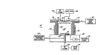
Referrins tc Fig. 1, a sput;r~r etching apparatus ,C
is i!lu5~r~te~ urilizin~ a uniqud induc ive
plasrna scurce l 2 of the invontion far sput.er~tching a~u~s~.ato
~aferl4. The sputteretching appt~-iratus tO cerr~pri~e~aa.3irl~ss
sreel ,,roce~s,n~ chamb~r 1~ which inclu~es a i~ase t~ and a
sLi~stra~e 3upFort or platen 2~ to hold sub5~rate 14 insice cf ,hs
cha~i~er 16 while it is bein~ sputtef etched.
rhc ~iub~;ratc ~upp~irt ~Gis c~pled tai ~n ~r po~r/~r
suppiy incllfding an R,C tuner 22 and prererc,bly a 13.56 MH.
~curCe 2~i. Thr~ ~o~rcr rr3y aper3te in ~ r~snge c' ~ipproxiimat~ly
- . g I M~tz to t i M~!z fsr suffic~en~ biaein~ cf ~he sur.,s.rate. ~urce
2¢ biases aubs~r3te 14 tci p,roduce skutter etching as describec~
fur1he~r hcreinbelc,~,v. Subs;ra~e supporr 2Q i~ aisa cauPlec to a
- backplane hoating gas supply 28 f~r providing bac!~plOne gas ;c
heat r~r c~ol .~ubstr~to 1 A. Sub~;trale sl.lppcrt 20 preferably
inciu~e~ channe!s formeri therein ~not showni ~r dis;ribu.inr.~ ;he
hea~;ing gas unifcrmly cver~he back~ide cf the sU~str~te 1 L
~ ~i'f~l'iO-,~ S;t~---
CA 02213771 1997-08-25
WO 96/30929 P~TnUS9~J~4433
Processing chamber 16 is closed and sealed at the top
end by a dielectric plate or window 30 which couples to the
stainless steel chamber 16 for a vacuum-tight seal. A vacuum
,oump 32 is coupled to the processing chamber 16 through base 18
to vacuum the internal processing space 34, which is created
adjacent substrate 14 by processing chamber 16 and dielectric
plate '30. A gas dispersing ring 36 is positioned around the top of
processing chamber 16 adjacent dielectric plate 30 and is coupled
to a plasma gas supply 38. The gas dispersing ring 36 disperses
0 the plasma gas uniformly around the processing space 34, and
specifically around substrate 14.
In accordance with the principles of the present
invention, the dielectric plate 30 includes a generally non-
conductive pocket portion or pocket 40, which is centrally disposed
in the plate 30 and extends downwardly from the top of chamber
16. Pocket 40 has a generally convex inner surface 41 which
project:s into processing space 34 toward substrate 14. Preferably,
the enltire dielectric plate 30 is non-conductive, but it is particularly
critical that poclcet 40 be non-conductive despite the construction
of the remaining portions of the plate 30. The non-conductive
pocket 40 extends from dielectric plate 30 into processing space
- 12-
CA 02213771 1997-08-2~
. vC~3l ~A~ F ' ''' ' ''
v ~ . L U ~
34 toward the substrate support 20 and subs~rat~ 14. Ta provite
energy to l~nite a~ld su~tain ~ plasma within the ~races~in~ sp~c~
~4, an inds~c~ive cail 42 is pcs~ti~ned outside the chamber 16
within the nan-conduc~ive pocXe~ ~10 a~ dielectric pl~te 30. As
S illustra~ed in Fi~u,e 1, inductive coil 42 is ~oun~ ar~und
l - inslde pac.~et 4C and is contoured to fo!law the generally auter
~:onc~v~ surfaca 43 of po~ket 4a.
Pocket ~0 prefera~iy hz3 a ~cnerally circul~r
tr~n6v~rs~ cr~s s~cticn ard the coil 42 follcws concave sur~ac
43 aro~,~nd pocket a,o for c,eating a uni'crm pl~sma ~round the
subs~r~c. ~9 the ccil ~2 Foll~w~ the outer concave sur;ace 43 of
poc~et 40, it forrns a contcure~ cail which is generally cr~nvex-
snaped in th~ direction of s~lb~rat 14 which extends inta the
processing sp3ce gen~rally ~o~Yially with poc~et 40 as sh~wn in
1~; Fig. 1. In o~c example, ~he packet ha~ a wall
thicknecs T cf apprcxim3teiy I g mm, a circumferenc~ C af
~pprcxintately 1 Q7 mm and ~ 1~3ngth L of ~pproxima~ly 1 SC~ mm.
The inductive c~il 42 is c~upled to an ~F power
supply, inc)uding an R~ tuner 4t, and ~retera~!y, a 430 i<Hz sourc~
~;o ~i. A tuner h~ing an operating r~ngs frorn 400 !CHz to 15 MHz
s~uld be gonerally us~ w~th ~he presem inveIlti~n as cl~imed to ~r~a~e a
CA 02213771 1997-08-2~ ilttNOEi~ SHE~T
L,U~ ,V ~r.i~ 3E~T ~5~ J7 : ~ o ~2 ~ .v ~
plasma. The RF curren~ from source 46 which fl~ws through
inductive ceil ~2 induces a tirn~ var~ing RF electric ~ield inside of
the prccessing spaca 34. ~ec~use p~cket 40 i~ non-co~uctive,
~he induc~ive elect,ic fi61d from ccn~oured coil 42 is coupl~d
.hro-~gh pac~cet 40 and t~en tO plasma gas from supply 3~, which
- ,3 a~spersed around pocket 49 and coil ~2 ~y ring 36. The
.nduc~ electric f~eld produced wllh~ the processin3 spac~ 3~
ionizes the gas and creates a dis~harge cf ionized 525 par~iclcs ar
plasme inct ~hown~ w~th~n the procPssing space 3~ ~nd pfoxim3te
13 subgtrat~ t1 Substrate 14 which is ~iased by F~F ~Gu~ce 74
artracts th~ ionized ~ p~rticles ~rcm the plasm~. an~ the par~lcles,
design~ted by arrows ~nd reference nume~l 4~, bcmbard ~he
upper surface 15 of ~he su~str3te 14 ta thereby sputter etch
sub3trate material away from the surf~ce l ~.
l'; It has been experimen~aily det~rrnined that the sh~pes
or poc.Y~t 4~ and con.aured inductive coil 42 creatr~ ~ uniforrr,
sputtering pi~sm~ heving a hi~h ~e~lsi~y of ic~nized gas partic~es 4~
proximata ~he upper.~ur~ace 15 of substrate ~. Su~strate surface
15 is bombard~d and the p~ese~t ~nvention ~s claimed produc~s a high urifor~n
2a 5put:er ~tching rate acrcss surf~ce 15, It has also been found that
~he non-c~ncluct;ve pocket 40 3s~d the contoured cGil 42, ~Ihich iS
14 ~
AA~ENDED SHEET
CA 02213771 1997-08-25
vvound around the outer concave surface 43 of pocket 40, provide
a high density uniform plasma over a large substrate surface.
~herefore, the present invention is particularly suitable for sputter
etching circular substrates having a diameter greater than or equal
to 0.203 m (eight inches) such as 300 mm substrates. Furthermore, it has
been experimentally determined that the plasma produced by the
pocket and contoured coil is stable and is repeatable for more
consistent sputter etching.
The construction design of the coil also would affect
1~ the plasma uniformity. For example, the coil 42 might be a spiral
coii as illustrated in the Figures or a zig-zag coil, or may even be a
single-turn coil. The wire used to form the coil 42 also would
affect the plasma. A wire having a circular cross-section is shown
in the Figures. However, a thin or flat wire might also be utilized in
accordance with the principles of the present invention.
Sputter etching apparatus 10 is electrically efficient
and utilizes RF tuners 22, 44 to reduce the reflected RF power from
the substrate support 20 and inductive coil 42, respectively. In a
preferred embodiment of the invention, a Faraday electrostatic
2û shield 50 is utilized around the coil 42 adjacent the outer concave
surface 43 of the dielectric plate poci<et 40 and between the coil
.
~A 02213771 1997-08-2~ AMENDE~ r-.'T
4Z and pocket 40. The electrostatic shield, which is preferably a
thin mesh, reduces the capacitive coupling of the inductive coil 42
to the plasma, and thus raises the efficiency of the coupling of
inductive energy to the plasma.
The uniform distribution of the plasma gas by ring 36
and the dense uniform plasma of the present invention produce
high uniform etch rates across large substrates. Furthermore, the
dense uniform plasma produced by pocket 40 and contoured coii
42 yields good etch results even at low vacuum pressures in the
range of 0.133 Pascais (1 mTorr). Still further, sputter etching apparatus 10
may be operated at very low wafer biasing voltages in the range of
approximately 50 volts, thus reducing sputter damage to the wafer.
The present invention is particularly suitable for substrates with
very fine devices and integrated circuit features having dimensions
ol approximately 2.5x10~7m (0.25 microns).
With pocket 40 and the contoured coil 42 of the
present invention, inductive energy is coupled to the plasma
through the top of chamber 16 and through dielectric plate 30.
Therefore, processin~ chamber 16 may be made of stainless steel,
instead of a dielectric material, such as quartz, because inductive
energy does not have to be coupled through the side walls of the
- 1 6 -
- -1
CA 02213771 1997-08-2~
T
lP, ~ ~ r C . ~
d ; rU-'1 '7-C'3 -~
pr~cess ir~s chamber 1~. The sputtrr 2tched material ~riginating
from substrate 14 adllerss rrto-e readily to st~inless steel than to a
dielectric ma~erial such as quartz; As 3 result, the inn~r wall of
the processing chamber ,l 6 mors readily holds the sputter etched
rnateri~l to prPvent flaking sf the marerial into the prccessing
ch~mber 34, thus reducing oontaminstion of rhe sputt~r ~tched
wa~er. rhe w311 ~l~y th~n ke c!eanr~d ~hen necessary to
remo~e the etched m~terial. Allernz~tiv~ly, a rn~t;~l ~hield, such as
shield 52, rn~y be ut~ ed between the irtner wail ~nd substrate
;C 14 to calch sput.er etched rnaterial. The ehield may be metal, such
as stainle~s steel, ar rrtay be made of a dielectric :T~tefial. Upon
reaching ~he end of its useful li~e, the shield _ may sir~ply be
rernoved and c!e~ne~ or discarded. The shield shculd not interfere
h the coupling Qf energy to ~he plasma, becausa energy ~5
coupled throug.~l the top ~fr th~ cham~er.
The inductiv~ con;oured coil 42 is ~rotected frcm the
etch envirQnment by pr.7eket 40, and thus. is nr~t exposed to the
sputter e~chinq process. This incrca~es t~te useful ll~e and reliabllity
of the coil 42 ~nd yields a more reliable sputter etching process.
Ta furthcr increast~ the uniformity and ~enslty of th~
sputtaring plasma, a magne~tc ring ~6 may bg u~ilized ~round the
CA 02213771 1997-08-25 ,~ c~ND~D SHirci
IF, VG~ e ~ I5AR ;,~ ' 7 '' ~
, ~ , , u ~ ~, 7 , ~U I i U ~ .~ 2 .1 ~
2 j992~ ;.;1 3
processing chamber 16 as illustrated in Figure 2. A rnagrletic ring
5O, ~hich preferably utilizes v~rticslly aligned elonsated regians
5 7, 5~ of altern3ting pclarity around th~ circumferenoe of the ring
~s iliustrated in Figure 2A, creates a magne~ic field within th~
prccerising sp~ce 34 ~djacent the inner wall af chamber 'l ~
The magnet 56 and masnetic field created th~reby have besn found
to pre~ ~nt pl~sma l~akagz by preventing diffusicn of ionize~ plasma
particies into w~ll of ch~mber 16, th~ls ~ielding a m~e un~farrn
pl,~sma~ Fur~hermor6. the ma5netiC field created by ring 56 ha~
lC b~en f~und ~o confina the plasma around s~l~p~r~ Z0 ~nd subst~ate
~, and IhUS increaseS thc d~nsit~ af the sPutter etching plas~a.
The shape of the non-conductive packe~ ~0 and th~
shape o~ the contoured COlj 12 may be vzri~d tQ imprcve plasma
charact~ristics within the prccessin~ space 3~. ~y varyin~ the
L5 depth sf pocicet 40 and the de~ree of curvature of the inner surfac~
41, ~nd by var~inq the resulting shape of tine ccntoured coil 4Z,
th~i plasma unifarmity and density ~re ;~ffe~t~d. It has been found
exp~riment~lly that the greater the pockel d~p~h and th~ c~nvexi~y
af the inner surfacs 41 and the greater the ~epth of coli 42, the
~en:er the uni~ormity of the res~Jltant pl~sma. I ioWeYer, as wil1 be
a~preciated by a pers~n ski'led in the ar~, the shape and dimensions
.
~VD~o~
CA 02213771 1997-08-25
~,~IP, ~ v,Y ~ c~ ; 1 v ~ i, u
d O i
-
of packet ~Q and ccil 42 may be tailcred F~ccarding ~o the
processing ch3rnbcr ~6, th~ in~ernal c~nfigurat,ans within ~hc
p-ocessing space 3~. as w~ll as the ~Ci7A ~n~ location of substrate
14. Fi~ur~ 1 shows an example, ~ot ~eing an ~?mbcdiment of the ~nvention, ~n whic~
pcckel ~0 is ge~erally cylindric~l ~d the coil. 4~ is c~ntoured and dimensicr3edt:c exterld ~Imos~ th.e en~ir~ IBngth of the proc~ssirlg charnber 16 to
terminctte ~ery ~'o~e ta substrat~ suppcrt 2Q an~ substri~r~ 11
f:igurr~ 2 sha~s a more shallow pocket ~0 and relaxed curvatur~ or
convexity af the Ir1ner surfacr~ 4~ and coil 4~. ~s illustra~ed in
f:igure~ 1 ana ~, th~ rasul~in~ sha,~e ct the con-t~uret coil 4~ is
~a,oen~nt upon the depth and shape of p~cke~ ~'0 and the ~hape
of ~he generally c~nca~e GUter, surfacc ~3.' The shape of the cail
:,~ ~y ran~ ~ywhere wirhin the sCope of the claims, for e,~mpl~
to a flatter convex-shaped coi~ ~s illu5trat~d in Figure 2. ~s wiil be
~S apprecia~d, ~ry sha~low pcckets utilize an induct~ve coii, which i5
almost flat or "pancake" in shape. ~ig. 2B sha:~rs a top ~iew of the
shape of the cc1!1 utili2ed in FiS;. 2.
To expl~in the ~n~raticn of ~he plasma source 12 af
the in~entioll as cl~med, all ex~?l~tion of the pl~sm~. igIt~ition scheme ~nd
~tching iS itelpflJI. Fi~.~re 3,4 is a sctlematic di~ram ~f the gas
flcw components f~r deli\~erin~ pl~sma gaS ta the prcc~ssin~
D
CA 02213771 1997-08-25
WO 96/30929 PCT~US9~;~14433
rhamber 16 and backside heating gas to the substrate support 20.
The gas flow components are synchronized to produce a gas
pressure burst for easy ignition of the plasma and to subsequently
create a sufficient gas flow to sustain the ignited plasma.
Figure 3B is a timing chart illustrating the operating
sequence and synchronization of the various gas supply
t,omponents illustrated in Figure 3A to produce pressure burst
ignition and a subsequent plasma. The gas flow system includes a
rnass flow controller 60 (MFC) for controlling the gas flow rate
~rom the gas supplies, such as plasma gas supply 38 or backplane
heating gas supply 26. Preferably, the gas used for both purposes
is Argon, and a single gas source may be coupled to mass flow
controller 60. An isolation valve 62 is coupled at the output of the
rnass Flow controller and may be incorporated with the structure of
the mass flow controller 60. After the isolation valve 62, the gas
supply line 64 is split between the backpiane branch 65 and a
procecising chamber branch 66. A needle valve 68 provides course
- adjustLrnent of the gas pressure in the processing chamber 16. The
c:hamber valve 70, in line with needle valve 68, provides a more
precise pressure control of the plasma gas pressure within the
procesising chamber 16. A backplane valve 71 controls the flow of
- 20 -
CA 02213771 1997-08-2~
WO 96130929 PCT~US95114433
~3as to substrate support 20 for backplane heating of substrate 14
duringi sputter etching. All of the gas flow components of Figure
3A and RF sources 24 and 46 are preferably coupled to a controller
59 for timed operation, except for needle valve 68 which is
rnanually opened and closed.
Referring to Figure 3B, the full process interval for
sputter etching a substrate may be divided into a pressure burst
interval denoted by reference numeral 72, a substrate power
-- interval denoted by reference numeral 73, a soft etch processinterval denoted by reference numeral 74, and a power down
interval denoted by reference numeral 75. As illustrated in line A
of Fig. 3B, a throttle 76, which is coupled to vacuum pump 32 (see
F-igs. 1 and 2) is kept closed, and the mass flow controller 60 is
opened for full gas flow at approximately 288 sccm, as illustrated
in line B. As illustrated in line C, the gas pressure in processing
c:hamber 16 begins to steadily rise due to the high flow of gas and
the absence of vacuum pumping. During the pressure build-up
within chamber 16, the isolation valve 62, needle valve 68, and the
c:hamber valve 70 are all open, as illustrated in lines 1, H, and G of
F-igure 3B in order to allow gas flow into the processing chamber
116. During the initial pressure build-up within pressure burst
- 21 -
CA 02213771 1997-08-2~
E'dF. ~ q ~5- ~5,~ ;J 7 ~ 7, i~ 7 ,.. i7u~ dZ ~ 1~/"
interval 72, nc backp!~ne sas i~ delivared to subs~ra~r~ suppart 2(~,
and ~her~fol~e, ~alve 71 is clc~ed ~line r). Furthermare, ~ho nF
power eo ;he induc-ive coil 42 is Qff ~llne ~) ~35;s the F.F etch
p~wer to ;.u~strat~ line E).. Refe~rin~ agOin to line C, when the
pfocossing chambef press~J~8 rises ~o a s~t p~int, e.g. 3.~ Pascals 130 mTarr),
de~ignated by roference nunleral ~6, controller 5g t~lrns on the hF
s~u~ce 46 to provide pawer to induc~r coil 42 (1in3 ol. ~n 80~
wat~ pcw~r set in~ for RF ~aurcs 4f~ has proven suff;ei~-nt to ignite
a pl~sm~ e appar~tus i0 of che mveIltion as cla~ned. ~Jpon the icn~tion of
;~ ~ plasm~, ~vhi~n is indlc3ted at the end of pressur~ ~urst interval
72. the throttle 75 ~o the vacuum pump 32 is open~od, and the ~as
flo~,v rate af the ~FC 60 i3 reduced l;irte 3), thus, caus~ng a drcp in
the processing chamber pressure ~line C~. rhe ~as ficw ;hrcugh
thrl MFC o0 is nlaintalned dt a level to sustain the iSnited plas,~.
. - iS The pawer to coil 4? ,line i}~ iS ~tjusted from the 8C0 ~a~t Isnition
levei belwean upper ana Ic~,ver level~ as shcwn to produco a
3uitahle ,clasma. Wi;hin the power-up intervaJ 73, controller 5~
turns an source 24 fcr etch~n~; subs~rate 1~. As illust. ated in line
~. the ~F sourca ~ has an assocl~3ted delay time t~ build up l0 tke
1~ d~sired autput le~ei, which may be ar5und 50 vc~lts. At the ~ime or
plasm3 iynition, the b~ckpiane vOlve 7~ i~ Qpenet ~o provide
- 22
A~EN~ED SHE~
CA 02213771 1997-08-25
W O 96/30929 PCTrUS95J14433
backside heating gas to substrate support 20 to heat substrate 14
i'line F). The processing chamber valve 70 is alternately opened
and closed during the sputter etching process to maintain a desired
(~as flow within the processing chamber. The plasma is sustained
and the substrate 14 is biased during the soft etch process interval
74. ~pon reaching a predetermined etch time, the power to the
substrate (line E) is shut off during the power down interval 75.
lrhe etch power to the substrate is shut off before the coil power
(line D) in order to determine the exact duration of the etch and to
,orevent damage to the substrate which may occur if the substrate
remains biased when the plasma power is turned off. As illustrated
in lines D and E of Figure 3B, both the RF coil source and the RF
s;ubstr,ate source have predetermined delays at their outputs when
s,witched off. At the end of the power-down interval 75, the mass
flow controller is closed (line B), the chamber valve is closed (line
Ci), and the isolation valve is closed (line H), thereby reducing the
glas pr~sssure (line C) in the processing chamber 16.
As illustrated in line A, the opening of the vacuum
tlhrottle 76 may be delayed if the gas flow and pressure within
chamber 16 is not sufficient to ignite a plasma. The delay is
illustrated by a dashed line in line A. Accordingly, the etch power
- 23 -
CA 02213771 1997-08-2~
.~lr, '~CA';~P~ S_SI .i,~ n~ 1?n3 ~ O
d ~ a
-
to substr~;P l 4 would also be delayed as Illustr~ted by the dashed
line in line E of Fisu~e 38.
The process~ng apparaius o~ the presen~ ~vent~a~ as ~l~med
provi~es a d~nse unifo~rn piasma ~o etch substrate 14. The
~pparatus is s~litable for su~trates utilizing srnail circ~uit te~ices
and features, and has a design which provi~es ~se of Se~'ViCe and
rn~ir~t~n~nce. r~ inventioll as claimed is capable ~f prcYiding su~ficie~tly
uniform and dense ptasmas acrr~ss large substr3tes ~t lower
pressufes and low su~rate ~iasinS vol~3ses.
iC In additi~n tc the aperation of pocket ~0 ~nd
contoufe~ coil ~, tt~e shape ~f the pccket and its depth of
extension intu the proce~s,rl~ spacc 34 may physi~ally ~ff~ct the
plasm~ to yield ~ mcr~ unitcrm etch. f~r example, a deep pocket
4~ as is illus;rated in Fi5. I mz~y physically aisplace the plasma
from ~bave the c~enter of sub5tr~te 1~ ta reduce ~he e~ch ratP at
the cen~r cf the sui~stf~te ~vhich is often higher ~han the etchrate
a1: ~he subs~r~e periphery. I herefore, ~he physic~l displ~c~ment
m~y ~ield ~ mor~ ~uniform etch. Further detailed disc~sian of sucn
a pla~m~ displacins ~ius is pro~ided in Hieronymi et ai., U. S.
2c Paten~ ,3~1,281 ~ss~J*d February 21, 1~5.
~ 24-
- ~sE~vDED SH~ET
CA 02213771 1997-08-25
The pockets 40 illustrated in the Figures are all
generally hollow and hold the co.ntoured coii 42. Alternatively, the
pocket 40 may be filled with a dielectric material or other suitable
material (not shown) which will surround the contoured coil 42 in
pocket 40 and thereby embed the coil therein.
While the present invention has been illustrated by a
description of various embodiments and while these embodiments
have been described in considerable detail, it is not the intention of
the applicants to restrict or in any way limit the scope of the
o appended c!aims ~o such detail. Additional advantages and
modifications will readily appear to those skilied in the art. The
in~ention in its broader aspects is therefore not limited to the
specific details, representative apparatus and method, and
illustrative examples shown and described.
~5
- 25 -
CA 02213771 1997-08-2~ 3