Note: Descriptions are shown in the official language in which they were submitted.
08/15/01 WED 10:35 FAg 41B 3s2 0823 RIDOLrT & MAYBES f~ 0o3
- 1 -
SYSTEM GENERATING DZ:SPLAY CONTROL SIGNALS ADAPTED TO THE
CAPABILITIES OF THE DISPLAY DEVICE
BACKGROUND OF THE INVENTION
Field of the Invention
The invention relates to a display system and,
more particularly, to a process of video data which is
supplied from an external image processing apparatus
and a display of an image regarding the video data.
Related Background .Art
In such a kind of apparatus, in recent years, when
displaying an image regarding image data outputted from
a computer, the realisation of a high resolution, the
registration of a display of a multicolor, and the
realization of a variety of kinds have been being
progressed.
For example, there is an apparatus in which the
number of display colors is also set to 16.70 millions.
These are a variety of kinds of [6~0 (horiaontal
display dots) x 480 (vertical line dots)], [S00 x 600],
[1024 x 768), [1280 x 1024], and [1600 x 1280]. A
resolution is also high,
In proportion to an increase in resolution, a
transfer cloak of a video signal which is transmitted
from a host computer to a display device is also high.
For example, in case of [1280 x 1024], a transfer
clock is set to 157.5 MHz at a frame rate (the number
of frames per unit time) of 85 Hz. In case of [1600
08/15/01 WED 09:36 [TX/RX NO 7175] f~ 003
CA 02213907 2001-08-15
CA 02213907 1997-08-25
- 2 -
1200], a transfer clock is set to 229.5 MHz at a frame
rate of 85 Hz.
There is a tendency such that the frame rate is
rising in order to reduce flickering. Further, there
is considered that a frequency of a pixel clock rises.
However, if the resolution and the frame rate are
merely raised as mentioned above, the following
problems occur.
First, when video data is received and processed
by a pixel clock of a high frequency, a heat generation
of an IC for performing a process increases and the
process cannot be accurately performed. When the user
intends to execute a process at a high precision, very
high costs are required.
In case of receiving video data by a pixel clock
of a high frequency, if the video data is received by a
long cable, many radiation noises in a high band are
generated, and a legal restriction cannot be cleared.
Such a problem becomes a large problem,
particularly, in case of displaying by a flat panel
display.
SUMMARY OF THE INVENTION
It is an object of the invention to solve the
problems as mentioned above.
Another object of the invention is to transmit
image data in accordance with an ability of a display
CA 02213907 1997-08-25
- 3 -
device, thereby enabling good process and display to be
executed.
To accomplish the above objects, according to an
embodiment of the invention, there is provided a
display apparatus comprising: display means for
displaying an image regarding video data which is
supplied from an image processing apparatus; storage
means for storing control information indicative of a
frame rate of video data which can be displayed by the
display means; and communicating means for transmitting
the control information read out from the storage means
to the image processing apparatus.
The above and other objects and features of the
present invention will become apparent from the
following detailed description and the appended claims
with reference to the accompanying drawings.
BRIEF DESCRIPTION OF THE DRAWINGS
Fig. 1 which is composed of Figs. 1A and 1B are
diagrams showing a construction of a display system as
an embodiment of the invention;
Fig. 2 is a diagram showing a construction of a
graphic controller in a host in Figs. 1A and 1B; and
Fig. 3 is a diagram showing a construction of a
display system to which the invention is applied.
CA 02213907 1997-08-25
- 4 -
DETAILED DESCRIPTION OF THE PREFERRED EMBODIMENT
An embodiment of the invention will now be
described in detail hereinbelow with reference to the
drawings.
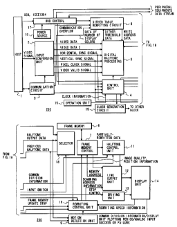
Figs. 1A and 1B are block diagrams showing a
construction of a display system according to the
invention.
The system shown in Figs. 1A and 1B in the
embodiment comprises: a host 1 to supply video data;
and a display device 200 for receiving the video data
from the host 1 and displaying an image regarding the
video data.
Functions of respective sections in Figs. 1A and
1B will be first described.
Reference numeral 1 denotes the host for supplying
the video data to the display device 200 and is mainly
made up of a personal computer, a workstation, or a
television. Reference numeral 2 denotes an input
conversion unit having: a function for receiving the
video data outputted from the host 1 and separating
horizonal and vertical sync signals from the received
video data; a function for converting analog data (for
example, assuming that the input video data is analog
data) into digital data; a demultiplexing function for
separating the video data so that it can be processed
in parallel in accordance with a transfer speed of the
video data; a function for detecting interlaced data in
the case where the host 1 outputs the interlaced data
CA 02213907 1997-08-25
- 5 -
as in a television or the like; and a function for
identifying a field number in the case where the video
data constructs one frame by a plurality of fields.
Now, assuming that the input data is digital data,
in the case where those digital data have been
multiplexed with respect to the time to thereby reduce
the number of transfer lines, a decoder for returning
the multiplexed data to the original data and a PLL for
generating a sampling clock of the multiplexed data are
included.
In the case where the display device can receive
any two or more of analog video data, digital video
data, and television data (NTSC, PAL, or the like),
selection data to select which data is inputted is
generated from the host 1 and is received by a control
unit 4 under the control of a communication circuit 3
or a hub control unit 17. The selection data is
outputted from the control unit 4 to the input
conversion unit 2.
The input conversion unit 2 switches the input
video data in accordance with selection information
from the control unit 4.
The communication circuit 3 receives information
regarding the video data which is supplied from the
host 1, for example, pixel clock frequency information,
frame rate information, identification information of
interlace/non-interlace, gamma correction data,
CA 02213907 1997-08-25
- 6 -
brightness, contrast, picture plane position
information, display mode (display dots, the number of
lines) information, foregoing identification
information of the video data, and the like.
Information of the frame rate of the video data
which can be displayed in the display device 200 and
information of a blanking period are transmitted to the
host 1.
The data communication between the host 1 and
communication circuit 3 is executed by using a two-way
serial communication.
Reference numeral 4 denotes the control unit for
controlling the display device. The control unit 4 can
perform an arithmetic operating process by a
microprocessor and can transfer input and output data.
Reference numeral 5 denotes a digital halftone
processing unit for dither processing input video data;
6 a dither table rewriting circuit for rewriting a
multivalue dither table and a dither threshold value
table in the digital halftone processing unit; 7 a
frame memory control unit for writing and reading
dither halftone data into/from a frame memory 8 arid for
reading data of a desired line from the memory as will
be explained hereinlater in accordance with an
instruction of a rewriting control unit 10; 9 a motion
detection unit for comparing dither halftone data of
the previous frame with dither halftone data outputted
CA 02213907 1997-08-25
_ 7 _
at present, thereby detecting a motion; 10 the
rewriting control unit for controlling the reading
operation of the memory in accordance with a motion
detection result by the motion detection unit 9 and
rewriting speed information from a display unit 14 in a
manner such that an image which is displayed on the
display unit is rewritten on a line unit basis; 11 a
halftone control unit for processing gradation data in
the case where a pixel has been divided into two or
more portions to the common side (horizontal
direction); 12 a line output unit for adding a scanning
address indicative of a display position on the display
unit 14 to the image data and for transferring the
resultant image data to the display unit 14; 13 a
driving unit which is controlled by the control unit 4
and line output unit 12 and drives the display unit 14;
and 14 the display unit having a matrix configuration
and comprising a display panel which is made of
ferroelectric liquid crystal having a memory
performance, a driving circuit, a back light, and the
like. The display unit 14 has therein an ROM in which
data that indicates the number of colors which can be
displayed, a resolution of a panel, a data transfer
period (corresponding to a frame period of the panel)
which is necessary for the display unit 14, and the
like and that is peculiar to each display unit has been
stored. This data is outputted to the control unit 4.
CA 02213907 1997-08-25
_ g _
Reference numeral 15 denotes an operation unit having
knobs which are used for the user to adjust a picture
quality and a position of a picture plane and a switch
to switch the on/off operations of a power source.
Reference numeral 16 denotes a power source and 17
indicates the hub control unit for supplying video data
or the like from the host 1 to the display device and
peripheral equipment connected to the display device.
The hub control unit 17 has a USB (Universal
Serial Bus) in which the use has recently been being
examined and an interface according to IEEE1394 as a
standard of a high speed serial bus interface. The hub
control unit 17 includes a switch to supply the data to
the display device and peripheral equipment connected
to the display device, a decoder of each data, an
interface with an external equipment, and the like.
Reference numeral 18 denotes a selector for
allowing the data received by the hub control unit 17
to be written into the memory 8 and to be displayed.
Reference numeral 19 denotes a clock generation circuit
for generating an operating clock that is necessary for
processing the video data in the display device. A
frequency of the clock generation circuit is controlled
by the control unit 4.
A display operation of the system in Figs. 1A and
1B will now be described.
When the power source is turned on by the
CA 02213907 1997-08-25
_ g _
operation of the operation unit 15, the control unit 4
reads out information regarding the data indicative of
the number of display colors which can be displayed by
the display unit 14 (this data includes common division
number data), a resolution, and data transfer period
(depending on the frame period of the panel) which is
necessary for the display unit 14 from the ROM provided
in the display unit 14.
On the basis of those information, the control
unit 4 calculates the minimum frame rate which can be
received by the display device and a blanking period
and transmits information of them to the host 1 through
the communication circuit 3. In the embodiment, the
information indicative of the frame rate is transmitted
to the host 1 in accordance with the power-on of the
display device 200 and, after that, it is never
transmitted at timings other than the case where the
power source of the display device 200 is again turned
on or where there is a request from the host at the
time of a change of the host.
The information of the pixel clock, frame rate,
and blanking period which is transmitted from the host
1 as mentioned above is received by the communication
circuit 3. The control unit 4 calculates a clock for
processing on the basis of those data and controls the
clock generation circuit.
When the information as mentioned above is not
CA 02213907 1997-08-25
- 10 -
received from the host 1, it is also possible to use a
default value (maximum system clock) or a frame rate
and blanking information which have previously been
held in the control unit 4 or a frame rate and a
blanking value which were set by the user via the
operation unit 15.
The control unit 4 outputs necessary data to the
dither table rewriting circuit 6 and halftone control
unit 11, respectively.
The dither table rewriting circuit 6 selects a
dither threshold value that is necessary for the
necessary number of display colors from a table which
has been prepared or calculates by arithmetically
operating a necessary table and rewrites the dither
threshold value table in the digital halftone
processing unit 5.
In this instance, the number of input bits can be
predetermined or can be determined by receiving such
information from the host 1 by the communication
circuit 3. It is also possible to calculate a display
mode in the input conversion unit 2 by using a
horizontal sync signal and to use input bits.
A rewriting timing of the dither table is not
limited to the timing when the power source is turned
on by the operation unit 15. The dither table can be
also rewritten when the display unit is changed, the
host is changed, or the display mode is changed.
CA 02213907 1997-08-25
- 11 -
After completion of the rewriting of the dither
table, the video data supplied from the host 1 is first
converted to the data of a format adapted to processes
at the post stage by the input conversion unit 2.
That is, for example, assuming that the input
video data is the analog video data for a CRT as
mentioned above, it is converted into the digital data.
In case of differential digital data, it is converted
to the data of a TTL level or a CMOS level. When a
transfer frequency of the input video data is high, for
example, when it exceeds 100 Hz, the video data is
demultiplexed, thereby reducing the transfer frequency
to the half frequency.
When the input video data is an interlaced signal
like a television signal, its discrimination signal and
an identification signal of a field number are
outputted.
As mentioned above, although a plurality of video
data are supplied to the input conversion unit 2, any
one of them is selected by the information derived by
the communication circuit 3 or hub control unit 17 and
is supplied to the digital halftone processing unit 5.
The video data which was dither processed by the
digital halftone processing unit 5 is written into the
memory 8. The video data which is written in the
memory 8 is sequentially updated so long as the writing
operation is not inhibited by the control of the
CA 02213907 1997-08-25
- 12 -
rewriting control unit 10.
On the other hand, the dither processed video data
is also outputted to the motion detection unit 9. The
video data of one frame before is also supplied from
the memory 8 to the motion detection unit 9
synchronously with the output of the video data from
the halftone processing unit 5. The motion detection
unit 9 obtains a difference between the video data of
the inputted two frames on a pixel unit basis. When
the differential value exceeds a certain threshold
value th, such a portion is detected as being a portion
with a motion (hereinafter, such a portion is also
referred to as a moving portion).
The detection result of the motion detection unit
9 is outputted to the rewriting control unit 10 and the
rewriting control unit 10 controls the memory control
unit 7 so as to read out the portion with the motion
from the memory 8. The memory control unit 7 reads out
the video data of the moving portion and supplies to
the halftone control unit 11.
When the moving portion is not detected by the
motion detection unit 9, in order to refresh the whole
picture plane, the rewriting control unit 10 controls
the memory control unit 7 so as to read out the video
data from the memory 8 in a multi interlacing or random
interlacing manner.
In case of a display device without flickering,
CA 02213907 1997-08-25
- 13 -
the refreshing operation can be also performed in a
non-interlacing manner.
The video data read out from the memory 8 as
mentioned above is outputted to the halftone control
unit 11. The halftone control unit 11 converts the
video data in accordance with the common division
number information outputted from the control unit 4
and supplies the converted data to the line output unit
12.
The line output unit 12 adds scanning address
information which is outputted from the rewriting
control unit 10 to the video data and supplies the
resultant data to the display unit 14. The scanning
address information is data indicative of a moving
portion designated for the memory 8 by the rewriting
control unit 10.
The line output unit 12 outputs data indicative of
a writing timing of the display unit 14 to the driving
unit 13. The driving unit 13 forms a driving signal
for driving the display unit 14 in accordance with its
timing and supplies it to a driver IC in the display
unit 14.
The display unit 14 rewrites an image of the line
designated by the scanning address on the basis of the
video data supplied from the line output unit 12, the
scanning address data, and the driving signal which is
supplied from the driving unit.
CA 02213907 1997-08-25
- 14 -
According to the embodiment as mentioned above,
prior to displaying the image, the frame rate at which
the image can be displayed by the display device and
the data indicative of the blanking are transmitted to
the host 1 and the host 1 generates the video data in
accordance with the frame rate and blanking data which
were transmitted from the display device.
The specific operation of the host 1 such that the
information such as frame rate, blanking, and the like
from the display device is received and the video data
is outputted will now be described.
Fig. 2 is a block diagram showing a construction
of a graphic controller 100 which is provided in the
host 1 and controls the operation to supply the image
data to the display device 200. The graphic controller
of Fig. 2 is connected to the input conversion unit 2
and communication circuit 3 in Figs. 1A and 1B by a
connector (not shown).
In Fig. 2, the frame rate and the blanking
information transmitted from the communication circuit
3 in Figs. 1A and 1B as mentioned above are received by
a communication circuit 104 and are held in a buffer
(not shown) in the communication circuit 104.
A control unit 103 calculates a frequency of the
pixel clock and reads out the video data from a memory
107 on the basis of the frame rate information and the
blanking information which were received by the
CA 02213907 1997-08-25
- 15 -
communication circuit 104.
That is, when the received blanking period is
longer than the blanking period of the video data which
is treated in the host, the blanking period is set to
the received blanking period. An arithmetic operation
is executed as follows by using the received frame rate
and, further, a resolution value that is set by the
graphic controller itself, thereby calculating the
pixel clock of the video data which is outputted to the
display device.
There is the following relation.
[(1/fp) x rh + bh} + by = (1/fv)
where, bv: vertical blanking
hv: horizontal blanking
fv: frame rate (frame frequency)
fh: horizontal frequency
rv: vertical resolution
rh: horizontal resolution
fp: pixel clock frequency
The control unit 103 calculates the pixel clock so
as to satisfy the above equation and changes frequency
dividing ratios of a frequency divider in a PLL 105 and
a programable frequency divider 106 in accordance with
a calculation result.
An oscillator 101 generates a clock of a
predetermined very high frequency. The PLL 105
includes a phase comparator, a counter, a loop filter,
CA 02213907 1997-08-25
- 16 -
and a VCO and generates a clock whose phase is
synchronized with the clock from the oscillator 101.
The control unit 103 controls the frequency
dividing ratio of the frequency divider even by
controlling a count value of the counter in the PLL 105
and allows a clock that is closest to the calculated
pixel clock to be outputted from the PLL 105.
The frequency divider 106 frequency divides the
pixel clock outputted from the PLL 105, generates a
horizonal sync signal, a vertical sync signal, and an
image valid signal, and supplies them to an adder 108.
On the other hand, video data from another video
data input source such as video camera, tuner, or hard
disk of the host 1 is supplied to the memory 107 and is
sequentially written into the memory 107 by a clock
according to an operating clock of the host 1.
In the reading mode, the video data is read out in
accordance with the frame rate and pixel clock which
were calculated by the control unit 103 as mentioned
above and is supplied to the adder 108.
That is, although the video data is written into
the memory 107 in response to the operating clock of
the host itself, when the video data is read out from
the memory 107, it is converted into the video data of
the frame rate and pixel clock according to the display
device.
When the calculated frame rate is lower than the
CA 02213907 1997-08-25
- 17 -
frame rate of the video data to be written into the
memory 107, the video data is thinned out in accordance
with its ratio and is supplied to the display device.
The adder 108 adds the horizontal and vertical
sync signals generated from the frequency divider 106
to the video data read out from the memory 107 and
supplies the resultant data to the input conversion
unit 2 in Figs. 1A and 1B.
The pixel clock signal from the PLL 105 is also
similarly supplied to the input conversion unit 2.
The control unit 103 outputs the frame rate
regarding the outputted video data, the blanking, and
the data regarding the pixel clock period to the
communication circuit 3 in the display device through
the communication circuit 104.
On the display device side, the processes as
mentioned above are executed on the basis of the
information transmitted in this manner and an image
corresponding to the video data is displayed.
When the frame rate is not transmitted from the
display device side, a frame rate and a pixel clock are
calculated on the basis of data which has previously
been stored in a video BIOS 102.
In the embodiment as mentioned above, the frame
rate at which the image can be displayed and the
blanking information are transmitted from the display
device side to the host and, on the host side, the
CA 02213907 1997-08-25
- 18 -
video data is supplied to the display device on the
basis of the transmitted information, so that it is
possible to prevent that the frequency of the pixel
clock of the video data to be transmitted rises
unnecessarily.
Therefore, a problem as mentioned above in
association with an increase in frequency of the pixel
clock doesn't occur. Even in any case, processes
according to the ability that is peculiar to the
display device can be executed and the video data can
be accurately processed.
In the above embodiment, the graphic controller
100 has been provided in the host 1. As shown in Fig.
3, however, it is also possible to construct such that
the graphic controller 100 is provided out of the host
1 and the graphic controller 100 and host 1 can be
disconnected through a cable 110.
With this construction, the foregoing function can
be also provided for a host without means for receiving
the frame rate information from the display device 200
as mentioned above.
In the above embodiment, the control unit 103
calculates the frequency of the clock by performing the
arithmetic operation by using the information of the
frame rate and the blanking transmitted from the
display device. However, the invention is not limited
to such a method but it is also possible to construct
CA 02213907 1997-08-25
- 19 -
in a manner such that an ROM table is provided in the
video BIOS 102 and the control unit 103 selects
parameters regarding a plurality of clocks written in
the ROM table on the basis of the inputted frame rate
and blanking information.
As described above, by transmitting the frame rate
of the video data which can be displayed to the image
processing apparatus, the video data is not
unnecessarily transmitted at a high speed.
By outputting the video data in accordance with
the frame rate of the video data which can be displayed
by the display device, the proper video data according
to the characteristics which are peculiar to the
display device can be outputted.
Many widely different embodiments of the present
invention may be constructed without departing from the
spirit and scope of the present invention. It should
be understood that the present invention is not limited
to the specific embodiments described in the
specification, except as defined in the appended
claims.