Note: Descriptions are shown in the official language in which they were submitted.
CA 02214023 1997-08-27
W 096/27407 1 PCTAUS96/02110
PACKAGE INTEGRATED ACCELEROMETER
BACKGROUND OF THE INVENTION
~, The present invention relates generally to implantable cardiac pacemakers, and in
5 particular to a method for surface mounting a piezoceramic accelerometer directly to a
hybrid circuit thereon within a hermetically sealed pacemaker housing.
Present day piezoceramic cantilevered beams are well understood in the area of
cardiac pacing, as well as the equations which govern their char~cteri~tics. Conventional
electrical and mechanical connection of the beam is typically clamped on the short edge of
10 the beam producing a cantilever configuration, which defines the overall beam length.
U.S. Patent No. 4,140,132, issued to Dahl describes one of the first uses of
piezoceramic m~teri:~l as a physical activity sensor. The issued patent describes an
elongated piezoelectric cantilevered element with a weighted mass on one end of the
element enclosed within an impl~nt~cl cardiac p~cf m~ker.
U.S. Patent No. 5,235,237, issued to Leonhardt discloses a piezoceramic bending
beam accelerometer enclosed within a housing and employs surface mount technology for
mounting the packaged accelerometer by clamping do~,vn one end of the accelerometer
within the enclosed package.
U.S. Patent No. 4,653,326, issued to Danel et al. cites an accelerometer capable of
20 mez~ ring a co~ ol~llL of acceleration by means of a variable capacitance capacitor.
U.S.PatentNo.5,031,615,issuedtoAltcitesapacemakerwhichemploysan
accelerometer cnmpri.cing a mini~tnri7~cl mechanoelectrical converter or lr~n~ cer formed
in a semiconductor device.
However, the aforementioned disclosures have disadvantages. For example, the
25 beam c~nntoctinn to the package or pacemaker shield becomes a clo. l . i . .~ factor in
d~ ....; .. i ..p the st~ilivily output of the accelerometer when employing a bonding medium
of either solder or contlllctive epoxy. When bonding, the me~ m may bleed onto the beam
resllltinp in a reduced effective net length of the beam and an ~ l ion of piezoceramic
sensitivity. Hence, the bonding step can adversely affect the overall bearn p~-r~l.--ance and
30 contribute to m~mlf~-tllring yield loss. Also, the bonding method, supra, requires complex
and ~ sive p~ ing techniques to ensure a robust design.
CA 02214023 1997-08-27
W 096/27407 2 PCTrUS96/02110
SU M M A~RY OF THE rNrVENTION
The present invention overcomes the disadvantages of the prior art by providing a
method of and a~p~Lus for coupling an accelerometer within a cardiac pacemaker. The
way in which this solution is achieved by the invention will be understood by considering
the following description.
In a ~ler~lled aspect, the present invention provides a cardiac pslrem~ker with a
piezoceramic accelerometer directly coupled to the p~c ~m~ker hybrid circuit thereto via
surface mount technology, (SMT).
More specifically, the accelerometer crystal is wider than the prior art with two
incisions made from the same side thereby forming three members. The outer members are
used for coupling the accelerometer crystal to the hybrid circuit and define the inactive
areas of the crystal. The third and center member clelint~tec the active area of the crystal,
that is, the piezoceramic cantilevered beam which generates an electrical signal based upon
patient activity. Unlike the prior art, the invention integrates the coupling members as part
of the accelerometer and renders an accelerometer design independent of the coupling
method employed.
In another aspect of the invention, the accele,rometer is custom packaged in a metal
housing prior to surface mounting to the hybrid circuit. Unlike the inherent disadvantages
associated with the prior art, -he inven~ion employs a custom package to contact only the
outer legs of the accelerometer thereby allowing the entire cantilever beam to move freely
within the z-plane of the sensor.
An advantage of the mêthod of the present invention is the outer ~limen~ ns can be
held constant and the electrical output signal can be me~hz~nic~lly adjusted by the depth and
width of the aforPmentinnlo-l incisions, thereby a family of accelerometer crystals of
dirr~ l~"lL outputs could employ the same package.
Another advantage of the present invention is the electrical output signal can be
further adjusted by the ~tt~ehment method. That is, by decreasing or increasing the bonding
area of the outer members of the hybrid adds or subtracts to the output signal of the sensor
respectively.
Yet another advantage of the present invention is the outer members provide an
option for a simple ~ttsll~hment of the sensor to a surface mounted package thereby
elimin~ting output signal variability due to the ~tt~hment of sensors without outer
members.
CA 02214023 1997-08-27
W 096/27407 3 PCTAUS96/02110
Moreover, Yet another advantage of the present invention is the electrical output
signal of the accelerometer can be functionally adjusted by reducing a small amount of
metalization from the top portion of the third member by laser trimmin~, thereby reducing
the effective net length.
The present invention is specifically concerned with a method of m~nllf~chlring a
surface mountable piezoceramic accelerometer, and in particular an accelerometer with
adjustable sensitivity which corresponds to the inventive shape ofthe sensor. The pl~f~ d
method involves surface mounting via a protective package to the hybrid circuit of the
pacemaker. This method further provides pre-circuit ~tt~rhment testing and adjlletmenf for
performance centering and yield enh~ncement. An ~ltPrn~tive coupling method is also
disclosed. The ~ltern~tive method of mounting is by direct surface mounting of the sensor
to the hybrid circuit of the p~c.Pm~ker.
Other features, advantages and objects ofthe piezoceramic accelerometer sensor
and method of m~mlf~cture of the present invention will hereinafter become more fully
~p~U~;lll from the following description of the drawings, which illustrate the invention.
BRIEF DESCRIPTION OF THE DRAWINGS
FIG. 1 is an illustration showing placement of a pacemaker in accordance with the
disclosed embodiment of the invention in a patient;
FIG. 2 is a block ~ gr~m of a pacemaker in accordance with the disclosed
embodiment of the invention;
FIG. 3 is a perspective view of a bimorph accelerometer in accordance with the
disclosed embodiment of the invention; and
FIG. 4 is a ~ gr~mm~tic representation of the process steps involved in an
exemplary embodiment of the method of the present invention.
FIG. 5 is an exploded perspective view of an impl~nt~hle medical device and the
electronics which are hermetically sealed by the device shields.
DESCRIPTION OF T~. PREFEI~RED EMBODIMENTS
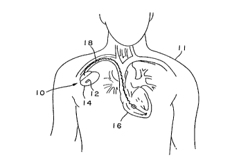
~ Referring to FIG. 1, there is illlletr~te-l the pl~Pment of a p~cPm~kPr 10 in
accul~lce with one embodiment of the present invention. P~cPm~ker 10 is shown in FIG.
1 as it would be implanted in a patient 1 1. The pler~ d embodiment of the invention
includes an activity sensor 12, which is a piezoceramic accelerometer disposed on the
hybrid circuit and isolated from the housing 14 of p~Pm~kPr 10. P~cPm~kPr 10 may
-
CA 02214023 1997-08-27
W096/27407 PCTrUS96/02110
additionally include other sensors~ such as a p~ sensor or the like implanted within
heart 16 or disposed on the distal end of pacemaker lead 18.
A p~Pm~ker which measures the physical activity of a patient by means of a
piezoelectric tr~nc~ er which is disposed on the housing of the p~Pm~k~r is disclosed in
U.S. Patent No. 4,485,813 to Anderson et al. and accignPrl to the :~ccignPe of the present
invention, which patent is incorporated herein by reference in its entirety. Also in U.S.
Patent No. 5.031.615 issued to Alt as disclosed~ supra, is another example of an activity-
sensing cardiac p~çPm~ker which uses an integrated mini~hlri7Pc~ accelerometer.
It is to be lln-lerctood that the present invention is not limited in scope to either
10 single-sensor or dual-sensor p~ççm~kPrs~ and that other sensors besides activity and
pressure sensors could be used in practicing the present invention. Nor is the present
invention limited in scope to single-chamber p~r~mz~kers. A multiple-chamber (e.g., dual-
chamber) p~em~ker can also be used in practicing the present invention.
Turning now to FIG. 2~ a block diagram illustrating the conctit lent components of a
15 pacemaker 10 in accordance with the presently disclosed embodiment of the invention is
provided. Although the present invention will be described herein in conjunction with a
pz~Pm:lkPr 10 having a microprocessor-based arçhit( ct-lre. It will be nn~lPrctood that the
present invention may be utilized in conjunction with other implantable medical devices,
such as cardioverters, defihrill~tors~ cardiac assist systems. and the like.
In the illustrative embodiment shown in FIG. 2~ p~l ~ m~kPr 10 includes an activity
sensor 12~ which as previously noted is a piezoceramic accelerometer bonded to the hybrid
circuit inside of the p~eem:~ket housing. Piezoceramic accelerometer sensor 12 provides a
sensor output which varies as a function of a measured parameter that relates to the
metabolic requirements of patient 11.
p~Pmz~kPr 10 of FIG. 2 is programmable by means of an external pro~ ",.-p
unit (not shown in the figures). One such programmer suitable for the purposes of the
present invention is the Medtronic Model 9790 programmer which is commercially
available and is int~ntl~ A to be used with all Medtronic p~rPm~kprs. The programmer is a
microprocessor device which provides a series of encoded signals to p~c~çmz~k~r 10 by
30 means of a pro~ ~" " "i ~ head which ~ l l l i L!i radio-frequency (RF) encoded signals to
p~c~mz~ker 10 according to the telemetry system laid out, for example, in U.S. Patent No.
5,312,453 issued on July 7, 1992 to Wyborny et al., which is hereby incorporated by
reference in its entirety. It is to be understood~ however, that the prog,~ ir.~
CA 02214023 1997-08-27
W 096/27407 PCTrUS96/02110
methodology disclosed in Wvborny et al. patent is identified herein for the purposes of
illustration only, and that any pro~ ."~.i.lp methodology may be employed so long as the
desired information is tr~n~mitte~l to the p~m~ker. It is believed that one of skill in the art
would be able to choose from any of a number of available pro~ I I I I I l; ~ .g techniques to
,~ 5 accomplish this task.
The programmer facilitates the selection by a physician of the desired parameter to
be programmed and the entry of a particular setting for the desired parameter. For purposes
of the present invention, the specifics of operation of the progr~mmer are not believed to be
important.
p~r~m~ker 10 is schem~tically shown in FIG. 2 to be electrically coupled via a
pacing lead 18 to a patient's heart 16. Lead 18 inel~lcle~ an intracardiac electrode located
near its distal end and positioned within the right ventricular (RV) or right atrial (RA)
chamber of heart 16. Lead 18 can carry either unipolar or bipolar electrodes as is well
known in the art. Although an application of the present invention in the context of a
single-ch~mher p:~rem~kt?r will be disclosed herein for illustrative purposes, it is to be
understood that the present invention is equally applicable in dual-chamber p~c~om~kers.
Lead 18 is coupled to a node 150 in the circuitry of p~m~ker 10 through input
c~p~citor 152. In the pl'est;lllly disclosed embodiment, piezoceramic accelerometer 12 is
~tt~h~l to the hybrid circuit inside ofthe p~em~ker 14 (not shown in FIG. 2), as noted
with reference to FIG. 1. As shown in FIG. 2. the output from piezoceramic accelerometer
12 is coupled to an input/output circuit 154.
Input/output circuit 154 contains the analog circuits for interface to heart 16~piezoceramic accelerometer 12, an antenna 156, as well as circuits for the application of
stim~ ting pulses to heart 16 to control its rate as a function thereof under control of the
software-implement--~l algoliLl--lls in a microcolll~uLtl circuit 158.
Microcolllpulel circuit 158 comprises an on-board circuit 160 and an off-board
circuit 162. Unit 158 may correspond to the microcolll~uL~l circuit employed in U.S.
Patent No. 5,312,453 issued to Shelton et al. on May 7, 1994., which is hereby incol~ol~l~d
by reference in its entirety. On-board circuit 160 includes a microprocessor 164. a system
clock circuit 166, and on-board RAM 168 and ROM 170. In the ~ llLly disclosed
embodiment of the invention, off-board circuit 162 cl)mpr~ c a RAM/ROM unit. On-board circuit 160 and off-board circuit 162 are each coupled by a data co.. l.. ic~tion bus
CA 02214023 1997-08-27
W 096/27407 PCTrUS96/02110
172 to a digital controller/timer circuit 174. Microcomputer circuit 158 may be fabricated
of a custom integrated circuit device slngmcnterl by standard RAM/ROM components.
It will be understood that the electrical components represented in FIG. 2 are
powered by an aL".Iupliate impl~nt~hle battery power source 176. in accordance with
common practice in the art. For the sake of clarity, the coupling of battery power to the
various components of F~Pnnz~ker 10 has not been shown in the figures.
Antenna 156 is connected to inputloutput circuit 154 for purposes of
uplink/downlink telemetry through RF ~ . . and receiver unit 178. Unit 178 may
correspond to the telemetry and program logic employed in U.S. Patent No. 4~566,063
issued to Thompson et al. on December 3. 1985 or in the above-referenced Wyborny et al.
patent. both of which are incorporated herein by reference in their entirety. The particular
pro~ ."",;"g and telemetry scheme chosen is not believed to be important for the purposes
of the present invention so long as it provides for entry and storage of values of rate-
response parameters discussed herein.
A VREF and Bias circuit 182 generates a stable voltage reference and bias currents
for the analog circuits of input/output circuit 154. An analog-to-digital converter (ADC)
and multiplexer unit 184 ~ipiti7f~c analog signals and voltages to provide "real-time"
telemetry intracardiac signals and battery end-of-life (EOL) repl~ement function.
The operating c~-mm~3n(1c for controlling the timing of p~- enn~ker 10 are coupled by
data bus 172 to digital controller/timer circuit 174 wherein digital timers and counters are
employed to establish the overall escape interval of the p~rf~m~ker as well as various
refractory, bl~nking, and other timing windows for controlling the operation of the
peripheral components within input/output circuit 154.
Digital controller/timer circuit 174 is coupled to sensing circuitry including a sense
amplifier 188, a peak sense and threshold measurement unit 190, and a
c~ e~l.old detector 192. Circuit 174 is further coupled to an electrogram (EGM)
arnplifier 194 for receiving amplified and processed signals picked up by the electrode
disposed on lead 18 which signals are l~:pl~llL~ e of the electrical activity of the patient's
heart 16. Sense amplifier 188 amplifies sensed electrical cardiac signals and provides this
arnplified signal to peak sense and threshold measurement ~il.;uiLI~ 190, which provides an
inrlie~tit~n of peak sensed voltages and the measured sense amplifier threshold voltage on
multiple con~ ctor signal path 67 to digital controller/timer circuit 174. The arnplified
sense arnplifier signal is then provided to cull~ ol/~ llold detector 192. Sense
CA 02214023 1997-08-27
W 096/27407 PCTrUS96/02110
arnplifier 188 may correspond. for example, to that disclosed in U.S. Patent No. 4~379~459
issued to Stein on April 12, 1983, incol~oldl~d by reference herein in its entirety. The
electrogram signal developed by EGM amplifier 194 is used on those occasions when the
implanted device is being interrogated by an external programmer, not shown! to transmit
5 by uplink telemetry a representation of the analog electrogram of the patient's electrical
heart activity, such as described in U.S. Patent No. 4,556,063, issued to Thompson et al.~
accign~l to the zlccign~ e of the present invention and incorporated herein by reference. An
output pulse generator 196 provides pacing stimuli to the patient's heart 16 through
coupling capacitor 198 in response to a pacing trigger signal developed by digital
10 controller/timer circuit 174 each time the escape interval times out, or an externally
transmitted pacing command has been received~ or in response to other stored comm~n~lc
as is well known in the pacing art. Output amplifier 196 may correspond generally to the
output amplifier disclosed in U.S. Patent No. 4,476~868 issued to Thompson on October
16, 1984 also incorporated herein by reference in its entirety.
While specific embodiments of input amplifier 188, output amplifier 196, and EGMamplifier 194 have been identified herein~ this is done for the purposes of illustration only.
It is believed by the inventors that the specific embodiments of such circuits are not critical
to the present invention so long as they provide means for g~n~r~ting a stimulating pulse
and provide digital controller/timer circuit 174 with signals indicative of natural and/or
20 stimulated contractions of the heart.
FIG.3 illustrates the m~nllf~rtllre of a piezoceramic accelerometer. The two sheets
of piezoelectric m~t~ri~l 30 and 32 are bonded together to form a bill~pol~h with a platinum
metal 34 between. This structure is then co-fired and subsequently nickel electrode layers
are 100 and 101 plated on the upper and lower surface of the bimorph sheet. Next. the
25 piezoelectric sheet is poled by conventional means to yield piezoelectric properties~ that is
the electrical axes are set during polling to established the ori~-nt~ti~ n of the electrical
properties. The sheet 107 is then cut up into smaller rectangular elements with a ceramic
cutting saw (not shown in the figures). The process of m~nllf~l tllring piezoelectric m~t~ ri~l
is well known and believed that one skilled in the art would be able to accomplish such a
30 task.
Next, the step of ~ fining active area 36, the cantilever beam, and inactive areas 38
which are employed to couple the accelerometer to the p~f ~m~k~r hybrid circuit is
~t;lr~Jlllled
CA 02214023 1997-08-27
W 096/27407 PCT~US96/02110
FIG. 3 shows a piezoceramic sensor 102. Incisions 103 and 104 are made which
separate the inactive and active areas of the sensor. The incisions into the piezoelectric
material are also employed to define the sensitivity of the sensor by controlling the
resulting beam width 105 and length 106. The accelerometer in FIG. 3 is then surface
5 mounted onto the hybrid circuit as shown in FIG. 5.
Turning to FIG. 5. a finished medical device (e.g.a cardiac p~cem~ker) is formed by
mounting one or more feed throughs 509 to one or more of the shield halves 505 and 507.
enclosing the internal electronics 501. (e.g. pulse generator cil1uiLly) including a
piezoelectric accelerometer 512. and the battery cell 503 within the shield halves 505 and
507. coupling the battery 503 to the circuitry. coupling the circuitry to the feedthroughs 509
and subsequently laser welding the shield halves together along their edges to form a
substantially hermetic enr.los~lre. A molded plastic connector block assembly (not
illustrated) Co~ g electrical connectors for ~tt~hment to the feedthroughs 509 is
typically installed thereafter.
In FIG. 5, the outer members 514 and 516 of the sensor permit direct ~tt~ehment to
the hybrid circuit during final assembly by employing either a solder reflow or a conductive
epoxy film, which provides an electrical connection to the bottom side electrode. thereby
elevating the sensor from the hybrid substrate surface and providing szlti~f~rtory vibration
space for the center member 518 to move in a perpendicular arc relative to the planar
surface of the sensor. Furtherrnore. the ~tt~ehm( nt process. supra, elimin~tes the variability
of the electrical output signal by providing a consistent :~tt~rhment means of the
accelerometer to the p:~rem~ker hybrid.
Moreover. the electrical output signal of the accelerometer can be functionally
adjusted by reducing a small amount of met~li7~til~n from the top portion of the center
member by conventional laser trimming, (not shown in the figures), thereby reducing the
effective net length.
F~eferrin~ now to FIG. 4, the outer members 49 of the accelerometer 12 are
employed to mount the accelerometer within a low cost pl~Lecli\~e package in accordance
with the preferred embodiment of the present invention is ~ gr~mm~tically illustrated. In
FIG. 4A, a Ni/Au plated lid 41 is formed into a "U" shape 43 to allow clearance for
perpendicular movement of the center member (cantilever beam) 36. The lids 41 and 45
have been formed to contact only the outer members of the "M" in 12. After the metal
housings are made and plated. a con-llletive epoxy 47 is added to lid 45. which contacts the
CA 02214023 1997-08-27
W 096/27407 PCTrUS96102110
outer members 49 of the accelerometer 12 in FIG. 4C. The epoxy 47 forms an electrical
contact between the nickel plated surfaces of the piezoelectric accelerometer and the metal
housing. The conductive epoxy also provides a m~rhzlnicz~l bond, which holds all three
pieces together and is cured under pre~ in FIG. 4D. wherein the latter curing step is
conventional to the present art. The center member 36 (active area of the accelerometer) of
the accelerometer 12is isolated from the pack~ging assembly. Once the assembly process
40 is complete as illustrated in FIG. 4E the device defines an accelerometer component
which can be tested and characterized prior to coupling one t~rmin~l 59 of the device with
solder 53 to the hybrid, (not shown in the figures), and electrically coupling by an
l 0 ultrasonic wire bond process the other termin~l 61 to the hybrid via a wire bond 55. Hence.
this protective p~rk~ging process cnh~nres ms~nl]f~rturing yields by obviating the
variability of the output signal by providing a consistent :~tt~rhment means of the
accelerometer to the protective package.
Moreover, the output signal may be ~ngmen~l~d to by a twisting movement at the
base of the sensor 35 which adds to the output signal generated by the center member 36.
The fashion by which the outer members of the sensor are bonded may add to the output
signal or subtract from the output signal. For example, if con~ ctive epoxy is applied from
the base of the sensor to the opposite end of the base of the sensor along the outer members,
this bonding method will reduce the twisting of the sensor at the base, hence subtract from
the overall output signal. As the epoxy is removed from the base towards the opposite end
of the base of the sensor along the outer members, this bonding method will increase the
twisting of the sensor at the base, hence add to the overall output signal.
While only a single embodiment of the invention has been illustrated and described.
it is not int~n~le~l to be limited by the aforementioned embodiment of the invention and the
following ~ltcrnz~tive embodiment should be considered.
A method of m~nnf~rtllring a sensor for a medical device by providing a bimorphic
piezoceramic substrate and sculpturing a first member and second member from thepiezocerarnic ~ub:,L ~I~, wherein the first and second members are integral and define a
sensor 520 for a m~lir~l device in FIG. SB. The first member 522 is employed to couple
30 the sensor within the medical device, and the second member 524 defines the active area of
said sensor, which is also known as the cantilever beam of the sensor. Both members can
be positioned to form a ~ùb~L~lLially "T" shape as shown in FIG. SB. Note that the
accelerometer 512 in FIG. SA can be replaced with piezoelectric sensor 520 in FIG. SB.
CA 02214023 1997-08-27
W 096/27407 PCTrUS96/02110
Although specific ernbodiments of the invention have been set forth herein in some
detail, it is to be understood that this has been done for the purposes of illll~tr~ti~n only, and
is not to be taken as a limitation on the scope of the invention as defined in the appended
claims. It is to be nn-l~.r.ctnod that various alterations, s--hstitl-tions, and modifications may
S be made to the embodiment described herein without departing from the spirit and scope of
the appended claims.