Note: Descriptions are shown in the official language in which they were submitted.
CA 02214109 1997-08-28
W O96~7212 PCTnUS96/02g20
~N IMPRO~nED ~ CF~ ~LB~T~RT~ Nu~T~T~T~
FIELD QF THE lNv~NlloN
The present invention relates to materials which are
ablateable by lasers of visual light and more particular-
ly to methods of using such materials in the fabrication
and customization of integrated circuits.
BACRGROUND OF ~HE I~fv~:NlloN
Integrated circuits are usually manufactured in
large runs. However it is frequently desirable to make
small runs of a specific integrated circuit, typically
for prototyping. US Patent 4,924,287, the disclosure of
which is incorporated herein by reference, describes a
customizable integrated circuit. Methods for customizing
of such integrated circuits are shown in US Patent
5,329,152, the disclosure of which is also incorporated
herein by reference.
Customizable integrated circuits typically have
predetermined portions which are adapted for modification
before being supplied to the end user. Such modifications
include, inter alia:
(a) electrically programing memory locations;
(b) cutting conducting links; and
(c) creating conducting links.
Customization by cutting of conductor links is
preferred since this method does not require extra cir-
cuitry on the integrated circuit as do electrically
programmable logic devices. Furthermore, pre-produced
links can carry a higher current density than created
links.
Two methods are mainly used to selectively cut
links. One method is to cut each link directly with a
laser be~m. However, direct cutting with a laser may
require high laser energy densities. Application of large
amount~s of laser energy to integrated circuit surfaces
may damage the integrated circuit.
CA 02214109 1997-08-28
~ 2920
W096~7212
A preferred method of customizing such circuits is
to coat them with a layer of laser sensitive ablative
material and to ablate the material at selected locations
using a relatively small amount of laser radiation. After
such ablation, the integrated circuit is etched using an
etchant or other etching method that does not remove the
ablative material, for example, by chlorine plasma etch-
ing. Thus, only areas previously ablated by the laser are
etched. Customizable areas typically include metal links
so that etching the links modifies the interconnections,
and therefore the function, of the integrated circuit.
It is also known to use a photolithographic method
wherein the integrated circuit is coated with a layer of
radiation sensitive material and exposed to a pattern of
ultra violet light, visible light, X-rays or to an elec-
tron beam. The coating material is developed and the
areas exposed to radiation are removed. The integrated
circuit is then etched as described above.
In practice, due to the characteristics re~uired of
them, very few materials are useful as laser ablative
coatings. An efficient laser ablative material should be
capable of absorbing a large portion of the laser energy
and in response thereto be transformed directly and
immediately to gas. Laser ablation sometimes causes the
material to explode. Explosion transforms part of the
material to gas, however, some of the material is also
blown away as particles. Some of these particles may fall
back on the chip and cover-up previously uncovered areas,
counteracting the ablation/explosion at these areas. An
effective laser ablative material should not form many
particles. The term ablation means that the material is
turned directly to gas, and very few particles are
formed.
It is also desirable that the resultant ablation
pattern be as close as possible to the irradiation pat-
tern and that Gnly small amounts of energy leak into the
CA 02214109 1997-08-28
PCTnUS96/02920
W O 96/27212
surrounding area and into the integrated circuit. Other-
wise, the definition of the geometry will be poor and the
integrated circuit may be damaged. Additionally, the
material should adhere well to substrates and provide
good coverage of step geometries used in microelectronic
circuits. Since the purpose of the coating is to protect
coated areas while etching the uncoated areas, it is
important that the material be resistant to at least one
method of etching, preferably a metal etching method.
An example of a material which has some but not all
of the previous properties is Arsenic Sulfide. Arsenic
Sulfide has most of the abovementioned properties, howev-
er, since it does not cover uneven surfaces very well it
is not as useful as other materials.
Laser ablative materials which are ablated by ultra
violet lasers are known in the art. For example, US
Patent 5,302,547 shows covering an integrated circuit
with a liquid polymer and ablating that polymer with
ultra violet light. However, these polymers are transpar-
ent to visible light and are not known to be ablateable
by visible light lasers.
Very few materials are known to be ablateable by
visible light. Visible light is preferred to ultra violet
light because laser technology supplies more efficient
and less expensive lasers in visible light wavelengths.
US Patent 5,329,152 discloses the use of amorphous
silicon as a visible light laser ablative coating materi-
al. Amorphous silicon is ablated by visible light lasers
and is partially resistant to etching by chlorine plas-
ma, which is used to etch metals. Thus, an integrated
circuit with exposed metal links can be customized by
using amorphous silicon as the ablative material.
One problem with amorphous silicon is its high
vaporization temperature (2355-C) - 1000~C over its
melting point which increases the tendency to explosion
and particle generation.
CA 02214109 1997-08-28
PCT~S96/02920
WO96127212
Plasma deposited polymers (PDP), which are described
in "Plasma Polymerization", by H. Yasuda, Academic Press,
Inc. 1985, have properties such as crack-filling,
chemical inertness and selective permeability which make
them useful for a variety of uses such as surgical pros-
thetics and semipermeable membranes. US Patents
5,320,875, 5,312,S29, S,283,ll9 and 5,308,649, the dis-
closures of which are incorporated herein by reference,
disclose methods of manufacturing and uses of PDPs.
PDPs are typically manufactured as follows:
First, a substrate is placed in a plasma chamber.
The chamber is then filled with a gas, such as methane,
at a low pressure, typically on the order of l torr.
Plasma is then created in the chamber, typically
using a radio frequency (RF) electric field which ion-
izes the gas. Consequently, a polymer layer is continual-
ly deposited on the substrate.
It should be understood that a PDP is not a direct
polymer of the gas used in the process. It is believed
that the gas breaks down in the plasma and gas precursors
and their compounds form the PDP which is then deposited
on the substrate (and on the walls of the chamber)~ The
deposition process is a combination of two processes, one
in which molecules hit the substrate and cling, and
another in which they do not cling, and may even cause
some material to be etched off the substrate. The temper-
ature of the substrate dictates the types of molecules
which are likely to cling to the substrate and the manner
in which they will be attached to the PDP already deposi-
ted.
The gas usually flows through the chamber at a rate
which determines the types of molecules that form in the
plasma and, consequently, the type of PDP deposited.
There are many other parameters which may affect the
deposited PDP, such as the distance of the substrate from
different portions of the plasma and the RF power used to
CA 02214109 1997-08-28
W O96f27212 PCTnUS96102g20
create the plasma.
The gas used is typically an organic compound.
However, some inert gases, such as argon, may be added in
order tQ speed up the deposition process. It has also
been observed that similar polymers can be created from
different starting materials.
CA 02214109 1997-08-28
WO96/27212 PCT~S96/02920
SUMMARY QF THE INVENTION
The inventors have discovered a method of depositing
a Plasma Deposited Polymer (PDP) which is laser-ablative
by laser light having a wavelength longer than ultra-
violet light, such as visible light.
In a preferred embodiment of the invention, the PDP
is deposited in the following manner:
(a) providing a plasma vacuum chamber;
(b) placing~ the substrate (typically, a silicon
wafer) on the cathode of the chamber;
(c) introducing a plasma into the chamber, said
plasma generated by applying Radio Frequency (RF) radia-
tion to an active gas, the power density used is
between .08 Watt*cm~2 and l.59 Watt*cm 2; and
(d) terminating the process when the PDP is deposit-
. ed on the substrate to the desired thickness.
Preferably, an inactive gas such as argon is added
to the active gas at a ratio between 3:7 and 7:3, prefer-
ably, at a ratio between 4:6 and 6:4; most preferably, at
a l:l ratio. Preferably the gas mixture is introduced
through the anode and turned into a plasma in the cham-
ber. Alternatively, the gas is first turned into a plasma
and then introduced into the chamber. The inactive gas
may be added before or after the active gas is turned
into a plasma.
The substrate is preferably maintained at a tempera-
ture below 70~C. A pressure of between 0.l and 2 torr is
maintained, preferably, between 0.5 and l.5 torr. The
inventors have found that a pressure of about l torr is
most preferred. The active gas used is preferably organ-
ic, preferably, a hydro-carbon; typically, ethylene is
used. The gas is introduced into the chamber at a flow
rate between l sccm and 50 sccm, preferably between l0
and 35 sccm and most preferably, about 20 sccm. Prefera-
bly,~ Ionization of the gas is achieved with an RF power
density between 0.15 Watt*cm 2 and l Watt*cm 2; most
CA 022l4l09 l997-08-28
W O96/27212 . PCTrUS96/02920
preferably, the power density is between 0.24 Watt*cm~2
and 0.48 Watt*cm 2, Preferably, the RF radiation is
continuous at 13.6MHz. However, other methods of applica-
tion of RF enegry may be used, such as pulsed RF radia-
tion at a frequency of 400MHz. Preferably the cathode is
8" in diameter. The distance between the cathode and the
anode is between 1.5 and 10 cm, preferably 3 cm.
A typical deposition time of approximately 10
minutes will produce a polymer of a typically desired
thickness of approximately 1~.
These parameters can be adjusted to create a polymer
having predetermined characteristics. Specifically, a
material with low specific heat, low heat conductivity, a
small difference between its evaporation temperature and
its melting temperature and high light absorption is
desirable, and is achieved utilizing the above parame-
ters.
A PDP deposited under the abovementioned conditions
has one or more of the following properties:
(a) the material is stable enough to act as a passi-
vation layer;
(b) when ablated by laser, preferably a visible
light laser, the material absorbs enough of the incident
laser energy directed at it so that underlying layers are
not damaged by laser energy;
(c) only areas directly illuminated by laser energy
are ablated;
(d) the material is ablative, i.e., it vaporizes
rather tnan explodes, so that very little debris is
formed on the substrate when the material is ablated;
(e) the material is ablated in response to relative-
ly low levels of energy;
(f) the material has good filling qualities, so that
it can be deposited evenly over non leveled geometries;
~ g) the material is insulative;
(h) the material adheres well to the substrate;
CA 02214109 1997-08-28
W O96/27212 . PCTnUS96/02920
(i) the material is resistant to at least some forms
of metal etching;
(j) the material is ablateable by e-beam; and
(k) the material is etchable by some means, which
preferably do not etch the structure of the underlying
integrated circuit.
Alternately, a PDP having a selected absorption
coefficient can be deposited by properly selecting the
power density used to generate said plasma.
There is thus provided according to a preferred
embodiment of the invention a method of customizing
integrated circuits:
providing an integrated circuit;
depositing a PDP on the integrated circuit; and
ablating the PDP at preselected locations using a
laser beam, preferably a visible light laser beam.
Preferably, the integrated circuit is then etched,
~ preferably by reactive ion etching, at locations underly-
ing said ablated loca_ions.
There is further provided in accordance with a
preferred embodiment of the invention a PDP ablateable by
visible light.
Also provided in accordance with a preferred embodi-
ment of the invention is an integrated circuit coated
with a PDP ablateable by visible light.
There is further provided in accordance with a
preferred embodiment of the invention a PDP deposited
according the above described deposition parameters.
CA 02214109 1997-08-28
W O 96~7212 -. PCTnUS96/02920
BRIEF DESCRIPTIQN QF THE DRAWINGS
Fig. 1 is a schematic of a vapor deposition chamber
as used in forming an ablative layer in accordance with a
preferred embodiment of the invention;
Figs. 2A-2C show an integrated circuit customized in
accordance with a preferred embodiment of the invention;
and
Figs. 3A-3D show ~n integrated circuit customized in
accordance with an alternative preferred embodiment of
the invention.
DESCRIPTION OF THE PREFERRED EMBODIMENTS
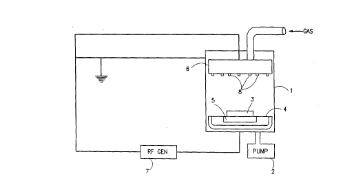
Fig. 1 shows a plasma vacuum chamber 1 suitable for
depositing a Plasma Deposited Polymer (PDP) on a sub-
strate, for example, a Plasma-Therm model 790 vacuum
chamber.
A substrate 3, to be coated with a PDP is placed in
chamber l! preferably on a cathode 4. The temperature of
substrate 3 may be controlled by a heater/cooler 5 such
that during deposition the sub_trate is maintained at a
substantially constant temperature. Preferably, the
substrate is maintaining at 20~C while the walls of the
chamber are heated. A pump 2 reduces the gas pressure in
chamber 1. Preferably, the pressure in the chamber during
the deposition is approximately 1 torr, however, pres-
sures between 0.1 and 2 torr are useful in carrying out
the invention.
A gas is supplied to chamber 1, preferably through a
plurality of nozzles 8 formed in an anode 6. The gas is
typically a mixture of an active gas, preferably an
organic compound such as ethylene or another hydro-carbon
and an inactive gas such as argon. Preferably, the ratio
between the active gas and the inactive gas is between
7:3 and 3:7, preferably, at a ratio of about 1:1. The
rate at which the gas mixture is supplied is called the
"flow rate" and is preferably between 1 sccm and 50 sccm,
preferably 20 sccm.
CA 02214109 1997-08-28
W 096~7212 . ~ 96/02920
Since many organic compounds and in particular:
C2H2, 6 6~ C6F6, C2H4, C2F4, Styrene, Cyclohexane
Ethylene oxide, Acrylic acid, Propionic acid, Vinyl
acetate, Methyl acrylate, Hexamethyldisilane, Tetrame-
thyldisiloxane, Hexamethyldisiloxane, Divinyltetramethyl-
disiloxane and many hydrocarbon compounds are known to be
interchangeable with ethylene in PDP deposition, a PDP
ablateable by visible laser light can be obtained if any
of the preceding organic materials are used, with appro-
priate changes in the deposition parameters, if required.
An RF generator 7, preferably operating at 13.6
MHz, is connected between anode 6 and cathode 4. For a
cathode diameter of 8" the power output of RF generator 6
is typically between 25W and 500W, preferably, between
75W and 150W. Preferably, anode 6 and (the walls of)
chamber 1 are grounded and a voltage differential appears
between them and cathode 4. The distance between anode 6
~ and cathode 4 is between 1.5 and 10 cm, preferably, 3 cm.
Alternatively, the active gas is turned into a
plasma in a separate compartment within the chamber. The
inactive gas may be added to the active gas before or
after it is turned into a plasma.
In a chamber configured as described above, a layer
of PDP is continuously deposited on substrate 3. Prefera-
bly, a layer having a thickness of about 0.6~ is deposit-
ed within less than 15 minutes.
It is to be appreciated that some other combinations
of values for the above parameters may also result in a
PDP being deposited and in some cases, the resultant PDP
may be ablateable by visible laser light.
A PDP deposited according to the abovementioned
configuration will be ablateable by visible laser light
and will have some or all of the following properties:
(a) low thermal conductivity;
(b) low evaporation temperature;
(c) an absorption coefficient of at least 3*103 cm~
CA 02214109 1997-08-28
. P ~ rUS96/02920
W O96~7212
in the mid-visible range;
(d) stability in Chlorine and Fluorine plasmas,
generally used to etch metal layers and insulation layers
respectively;
(e) ablateability at ambient conditions by visible
laser radiation (at 532 nm or 527 nm) at pulse energy
densities below 4 J/cm2;
(f) etchability in an oxygen plasma;
(g) capability of filling cracks which are approxi-
mately as wide as the layer of PDP;
(h) even deposition on the substrate;
(i) insulating capability;
(j) ablation without forming many particles at laser
energy above 1 J*cm 2;
(k) good conformance between the ablation pattern
and the laser radiation pattern;
(1) good adhesion to the substrate; and
~ (m) stability over a period of more than a year in
storage, so that the PDP can be used as a passivation
layer.
The inventors have also discovered that a PDP depos-
ited according to a preferred embodiment of the invention
has an evenly monotonicly decreasing absorption coeffi-
cient in the visible light range. Thus, it is easily
ablateable by ultraviolet light lasers and also ablate-
able by laser light in the near infra red.
A preferred use of a PDP having the abovementioned
properties is in customization of integrated circuits.
Figs. 2A - 2C show customization of an integrated circuit
in accordance with the present invention. Fig 2A shows an
integrated circuit which includes a metal layer 901,
separated from a second metal layer 902 by an insulation
layer 904. Layer 902 is also covered by a second insula-
tion layer 905, and another metal layer 903 covers layer
905. The entire top of the integrated circuit is prefera-
bly covered with a passivation layer 436. Since customi-
CA 02214109 1997-08-28
. PCTrUS96/02920
W O~6/27212
zation preferably includes disconnecting metal links in
layers 902 and/or 903, a plurality of apertures 422 are
preferably formed through passivation layer 436 and
through any intervening layers down to a metal link 438
that is to be disconnected. US Patent 4,924,287 to Orbach
and US Patent application serial number 08/290,550, filed
August 15, 1994 and titled "A Customizable Logic Array
Device", the disclosures of which are incorporated herein
by reference, both describe an integrated circuit pre-
ferred for customization.
A first step of the customization process, as shown
in Fig. 2A, includes depositing a layer 900 of PDP over
the integrated circuit. Preferably, the layer is 1~
thick. Since PDP layer 900 is preferably stable at ambi-
ent room conditions, the coated integrated circuit is
preferably manufactured in large runs and stored until
needed.
- A second step of the customization process, as shown
in Fig. 2B, includes ablating PDP layer 900 at selected
locations. Preferably these locations are over apertures
422. Preferably, a NdYAG frequency doubled laser at 532nm
or Nd YLF at 523nm is used for ablating PDP layer 900.
Alternatively an Argon laser at 514nm or at 488nm is
used. Preferably, the pulses are approximately 100 nano-
seconds long and have an energy density of approximately
4 J/cm2. The ablations can be performed using a laser
micromachining system, preferably, a QS650 available from
Chip Express (Israel) LTD.
A third step of the customization process, as shown
in Fig. 2C, includes etching the integrated circuit,
preferably, using Chlorine plasma.
Preferably, the remaining PDP is removed by Oxygen
plasma and a passivation layer is formed over the cus-
tomized integrated circuit.
Figs. 3A-3D show an alternative preferred customiza-
tion process similar to the abovedescribed process. In
-
CA 02214109 1997-08-28
PCTnUS96102920
W O96~7212
this embodiment, the integrated circuit is first coated
with a planarization layer 906, preferably silicon diox-
ide or other insulating planerizing materials as well
known in the art, before the step of depositing PDP
layer 900 thereon (Fig. 3A).
Fig. 3B shows the device after layer 900 is ablated
at selected locations.
An additional step of etching planarization layer
906, preferably with CF4 plasma is preformed (Fig. 3C)
before etching the integrated circuit itself (Fig. 3D).
The abovedescribed customization processes can be
carried out on most kinds of integrated circuits, includ-
ing CMOS devices, gate arrays, multi-chip packages and
memory chips.
Additionally, the inventors have found that the
ablation pattern of the PDP is very similar to the irra-
diation pattern used, so that very precise micromachining
of the PDP is possible. The depth of the cut is con-
trolled with a precision of 0.3~ or better. The radius of
curvature at the corners of rectangular cuts is 0.2~ or
less, even though a wavelength of .532~ was used. This is
attributed to the threshold nature of the ablation proc-
ess and to the properties of imaging with laser coherent
light.
The inventors have found that the PDP is more
versatile than using st~n~rd photo-resists because it
does not need to be developed and washed away. Further-
more, the inventors has discovered that the optical
properties of the PDP, in particular absorption, can be
controlled by changing the RF power used to ionized the
gas, therefore, a PDP layer with the correct absorption
can be produced for any chosen laser wavelength and any
desirable film thickness. Additionally, the etch resist-
ance properties of the PDP are similar to those of stand-
ard photo-resists.
It will be appreciated by persons skilled in the art
CA 02214109 1997-08-28
PcT/u~ 2520
WO 96127212
14
that the present invention is not limited to what has
been thus far described. Rather, the scope of the present
invention is limited only by the following claims: