Language selection

Search

Patent 2214130 Summary

Third-party information liability

Some of the information on this Web page has been provided by external sources. The Government of Canada is not responsible for the accuracy, reliability or currency of the information supplied by external sources. Users wishing to rely upon this information should consult directly with the source of the information. Content provided by external sources is not subject to official languages, privacy and accessibility requirements.

Claims and Abstract availability

Any discrepancies in the text and image of the Claims and Abstract are due to differing posting times. Text of the Claims and Abstract are posted:

  • At the time the application is open to public inspection;
  • At the time of issue of the patent (grant).
(12) Patent: (11) CA 2214130
(54) English Title: ASSEMBLIES OF SUBSTRATES AND ELECTRONIC COMPONENTS
(54) French Title: ENSEMBLES DE SUBSTRATS ET DE COMPOSANTS ELECTRONIQUES
Status: Deemed expired
Bibliographic Data
(51) International Patent Classification (IPC):
  • H05K 1/18 (2006.01)
  • B23K 35/26 (2006.01)
  • H05K 3/34 (2006.01)
  • B23K 35/00 (2006.01)
(72) Inventors :
  • BILTON, DAVID (Canada)
  • HAMILTON, MURRAY W. (Canada)
  • TRUMBLE, WILLIAM PATRICK (Canada)
(73) Owners :
  • NORTEL NETWORKS LIMITED (Canada)
(71) Applicants :
  • NORTHERN TELECOM LIMITED (Canada)
(74) Agent: DE WILTON, ANGELA C.
(74) Associate agent:
(45) Issued: 2003-12-02
(22) Filed Date: 1997-08-28
(41) Open to Public Inspection: 1998-03-19
Examination requested: 1999-07-16
Availability of licence: N/A
(25) Language of filing: English

Patent Cooperation Treaty (PCT): No

(30) Application Priority Data:
Application No. Country/Territory Date
08/719,300 United States of America 1996-09-19

Abstracts

English Abstract


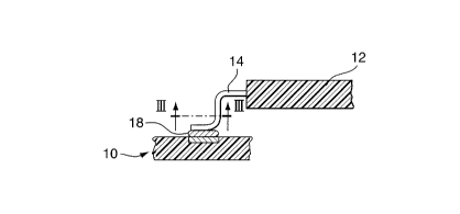
An assembly of a substrate and an electrical or
electronic component, the component having electrically
conductive leads with surfaces of an alloy of tin and
copper and the leads being soldered to copper based
terminals of the substrate by a solder alloy of tin and
copper. Lead solder is thus avoided. Preferably each
conductive lead has a surface layer of the alloy of tin and
copper and core within the surface layer of another
material which remains solid at the soldering temperature
of the surface layer. Also included is a method of
soldering a component with electrically conductive leads
having surfaces of tin and copper alloy to copper based
terminals by a solder alloy of tin and copper.


French Abstract

L'invention est un ensemble constitué par un substrat et un composant électrique ou électronique, ce composant ayant des conducteurs à surface en alliage d'étain et de cuivre qui sont soudés à des bornes à base de cuivre du substrat au moyen d'un alliage de soudure d'étain et de cuivre. On évite ainsi la soudure au plomb. Dans la concrétisation privilégiée de l'invention, chaque conducteur a une couche de surface en alliage d'étain et de cuivre et, sous cette couche de surface, une âme faite d'un autre matériau qui reste solide à la température de soudure de la couche de surface. Une méthode est également révélée pour souder à des bornes à base de cuivre, au moyen d'un alliage de soudure d'étain et de cuivre, un composant ayant des conducteurs électriques à surfaces en alliage d'étain et de cuivre.

Claims

Note: Claims are shown in the official language in which they were submitted.


-6-

WHAT IS CLAIMED IS:

1. An assembly of a substrate and an electronic
component wherein the substrate has a plurality of
terminals and the component has a plurality of electrically
conductive leads each of which comprises a core provided
with a surface layer consisting of an alloy, the surface
layer having a soldering temperature;

the electrically conductive leads being soldered to
the terminals by means of a solder alloy consisting of a
binary eutectic alloy of tin and copper, having a
composition of 99.3% by weight of tin and 0.7% by weight of
copper and having a melting point of 227°C;

the soldering temperature of the surface layer of the
core being at or above 227°C, and the core of each of said
electrically conductive leads being of a material which
remains solid at the soldering temperature of the surface
layer.

2. An assembly according to claim 1 wherein they core
comprises an alloy of tin, silver and copper alloy or
silver palladium alloy.

3. An assembly according to claim 1 wherein the
surface layer of the core is provided by a eutectic alloy
of tin copper having a composition of 99.3% by weight of
tin and 0.7% by weight of copper having a melting
temperature of 227°C.

4. An assembly according to claim 1 wherein the
soldering temperature of the surface layer of the core is
between 227°C and 240°C.

Description

Note: Descriptions are shown in the official language in which they were submitted.


CA 02214130 1997-08-28


ASSEMBLIES OF SUBSTRATES AND ELECTRONIC COMPONENTS
This invention relates to assemblies of substrates
and electronic components.
In conventional assemblies of substrates and
electronic components, electrical circuitries carried by
the substrates have termin~ls for connection to electrical
terminal leads of the components. For this purpose, a
solder is used which has a lead constituent. These lead
containing solders are known to be largely reliable for
0 forming permanent electrically conductive solder joints
between terminals and electrical conductive leads.
However, lead, it is now realized, is an undesirable
material to be used in industry. When used in solder, it
is not a captive constituent of the solder material and is
known to be environmentally unfriendly and is toxic.
Conceivably it is dangerous for use both by the
manufacturing worker and by the consumer. Lead presents
health hazards in manufacturing, disposal, and use of
assemblies, and problems arise in the safe disposal of
scrap materials containing lead.
Various assemblies have been made in which
leadless solder has been used. However, problems are found
during manufacturing where lead is not a component of
solder as resultant solder joints are found to be
unreliable as separation and cracking occurs.
The present invention seeks to provide an assembly
of substrate and electronic component which minimizes or
overcomes the above lead free solder problems.
Accordingly, the present invention provides an
assembly of a substrate and an electrical component wherein
the substrate has a plurality of copper based terminals,
the component has a plurality of electrically conductive
leads having surfaces comprising alloys of tin and~copper,
and the electrically conductive leads are soldered to the
terminals by means of a solder alloy of tin and copper.

CA 02214130 1997-08-28


In the assembly in a preferred and practical
arrangement, each of the electrically conductive leads has
a conductive body with a surface layer of the alloy of tin
and copper and the conductive body necessarily remains
solid, i.e., unsoftened, at the softening temperature of
the coating.
The solder must be such that during rise in
temperature, it comprises a pasty constituent for soldering
purposes at or around a specific temperature, and will
solidify to provide a solder joint immediately upon removal
of heat. A solder alloy having these requirements is
provided by tin having a weight percent at or around 99.3
of the total weight of the solder and with the copper being
at or around 0.7% of the total weight of the solder. It is
also preferable that the alloy in the coating of each
electrically conductive lead has approximately the
percentage weights referred to above of the constituent
parts are copper and tin. Hence, the coating and the
solder are in the same physical pasty state at soldering
temperature. This temperature is at approximately 227~C.
A flux to be used with the above solder according
to the invention must be compatible with the solder. It
must also be a flux which is operable at the desired
soldering temperatures which are envisaged for the
invention. An organic no-clean flux is considered to be
most desirable and this flux is one which should be active
at the temperature which the solder alloy has the pasty
constituent, i.e. around 227~C, and will successfully
remove oxides of copper and tin. Such a flux suitable for
this purpose is that referred to as X39 flux manufactured
by Multicore Solders Inc. of Richardson, Texas.
One embodiment of the invention will now be
described, by way of example, with reference to the
accompanying drawings, in which: -


CA 02214130 1997-08-28


Figure 1 is a plan view of part of a printed
circuit board having an electronic component mounted
therein;
Figure 2 is a cross-sectional view taken along
line II-II in Figure 1 and to a larger scale of part of the
printed circuit board and showing one of the leads of the
component secured thereto; and
Figure 3 is a cross-sectional view of the lead
taken along line III-III in Figure 2 and to a larger scale.
o In the embodiment as shown by Figures 1, 2 and 3,
a substrate comprises a printed circuit board 10 having
mounted therein a plurality of surface components 12 only
one of which is shown by the drawings. Each of the
components 12 has leads 14 which are soldered to terminal
pads 16 (Figure 2) of the printed circuit board 10. In the
embodiment as in the invention, the structure avoids the
use of lead materials in the solder to be used for
attaching the terminals permanently to the terminal pads
16. Thus, in the embodiment solder 18 located between ends
of the leads 14 and the terminal pads 16 is composed of a
solder alloy of tin and copper. This alloy in this
instance has a quantity of tin with a weight percent at or
around 99.3% of the total weight of the solder with the
remainder of the solder, i.e. 0.7% of the total weight,
being copper. The solder is compatible with the copper
terminal pads 16 so that a soldering operation will
permanently attach the solder 18 to each of the terminal
pads.
It is also necessary for the solder to be
compatible for soldering purposes to the surface material
of each of the leads 14. With this object in mind, each of
the leads is formed from a core 20 having a coating of a
material which is compatible with the solder. This coating
22 in this particular case is provided by a tin copper
alloy which is preferably of the same composition as the
solder alloy 18. In this case, the coating 22 on each of

CA 02214130 1997-08-28


the leads 14 is an alloy having tin with a weight percent
of around 99.3 of the total weight of the coating with the
remainder of the coating, i.e. 0.7% of the total weight,
being formed from copper. It is essential that the core 20
of each of the leads should be formed from a material which
not only is capable of supporting the coating 22 but also
one which remains in an unsoftened or unmelted condition at
soldering temperatures. Thus, in this particular
embodiment, each of the cores 20 may be formed from an
lo alloy of tin, silver and copper alloy or an alloy such as
silver palladium alloy.
During the soldering process, which may be by wave
soldering, reflow soldering or wire bond soldering
techniques, the solder alloy has a pasty constituent which
rapidly forms at a specific temperature around 220QC or
between 227 and 240QC and which upon removal of the heat
immediately returns to a solid condition. This sudden
return to a solid condition is particularly important in
that accuracy in fixed location of each of the leads 14 of
the electronic component upon the board is an absolute
necessity when subsequent process steps are to be followed
after the soldering operation. In addition, the flux which
is to be used needs to be compatible with the solder, the
terminal pad 16 and with the coating layers 22. Such a
suitable flux is that known as flux X39 made by Multicore
Solders Inc. of Richardson, Texas. This flux is known to
be active at temperatures of around and slightly above
227QC for removal of copper tin oxides from metal surfaces.
It is found that after the soldering operation,
the solder 18 efficiently solders each of the leads 14 to
the terminal pads 16. As the material of the coating
layers 22 is the same as the solder 18, then there is a
fusion between the pads 18 and the coating layers 22 so
that at their interfaces, the layers 22 and the solder 18
become metallurgically integral. Integrity of the solder

CA 02214130 1997-08-28


also takes place between the solder 18 and the terminal
pads 16 through the copper constituent of the solder.
It is found that with the above construction, an
efficient solder junction is provided between each of the
leads 14 and its terminal pad 16. The solder junction in
each case is reliable in manufacture and is not known to
crack or break away. In addition to this of course the
main object of the invention is realized in that the use of
lead as a component of solder is avoided together with its
lo attendent manufacturing use and scrap disposal problems.

Representative Drawing
A single figure which represents the drawing illustrating the invention.
Administrative Status

For a clearer understanding of the status of the application/patent presented on this page, the site Disclaimer , as well as the definitions for Patent , Administrative Status , Maintenance Fee  and Payment History  should be consulted.

Administrative Status

Title Date
Forecasted Issue Date 2003-12-02
(22) Filed 1997-08-28
(41) Open to Public Inspection 1998-03-19
Examination Requested 1999-07-16
(45) Issued 2003-12-02
Deemed Expired 2005-08-29

Abandonment History

There is no abandonment history.

Payment History

Fee Type Anniversary Year Due Date Amount Paid Paid Date
Application Fee $300.00 1997-08-28
Registration of a document - section 124 $100.00 1998-02-18
Request for Examination $400.00 1999-07-16
Maintenance Fee - Application - New Act 2 1999-08-30 $100.00 1999-07-16
Registration of a document - section 124 $0.00 2000-02-02
Maintenance Fee - Application - New Act 3 2000-08-28 $100.00 2000-05-25
Maintenance Fee - Application - New Act 4 2001-08-28 $100.00 2001-07-26
Maintenance Fee - Application - New Act 5 2002-08-28 $150.00 2002-08-19
Registration of a document - section 124 $0.00 2002-10-30
Maintenance Fee - Application - New Act 6 2003-08-28 $150.00 2003-07-31
Final Fee $300.00 2003-09-11
Owners on Record

Note: Records showing the ownership history in alphabetical order.

Current Owners on Record
NORTEL NETWORKS LIMITED
Past Owners on Record
BELL-NORTHERN RESEARCH LTD.
BILTON, DAVID
HAMILTON, MURRAY W.
NORTEL NETWORKS CORPORATION
NORTHERN TELECOM LIMITED
TRUMBLE, WILLIAM PATRICK
Past Owners that do not appear in the "Owners on Record" listing will appear in other documentation within the application.
Documents

To view selected files, please enter reCAPTCHA code :


To view images, click a link in the Document Description column. To download the documents, select one or more checkboxes in the first column and then click the "Download Selected in PDF format (Zip Archive)" or the "Download Selected as Single PDF" button.

List of published and non-published patent-specific documents on the CPD .

If you have any difficulty accessing content, you can call the Client Service Centre at 1-866-997-1936 or send them an e-mail at CIPO Client Service Centre.


Document
Description 
Date
(yyyy-mm-dd) 
Number of pages   Size of Image (KB) 
Abstract 1997-08-28 1 21
Cover Page 1998-03-27 1 47
Description 1997-08-28 5 210
Representative Drawing 1998-03-27 1 4
Claims 2003-04-10 1 37
Cover Page 2003-10-29 1 35
Drawings 1997-08-28 1 14
Claims 1997-08-28 2 65
Claims 2002-10-10 1 38
Fees 2000-05-25 1 31
Fees 2002-08-19 1 29
Assignment 1997-08-28 3 92
Correspondence 1997-11-04 1 33
Assignment 1998-02-18 3 115
Prosecution-Amendment 1999-07-16 1 30
Assignment 2000-01-06 43 4,789
Assignment 2000-08-31 306 21,800
Prosecution-Amendment 2002-06-18 2 40
Prosecution-Amendment 2002-10-10 2 69
Prosecution-Amendment 2003-01-09 1 31
Prosecution-Amendment 2003-04-10 2 68
Fees 2003-07-31 1 25
Correspondence 2003-09-11 1 29
Fees 2001-07-26 1 28
Correspondence 2004-11-15 2 135
Fees 1999-07-16 1 33