Note: Descriptions are shown in the official language in which they were submitted.
CA 02214869 1997-09-08
1 P/60887.CAP/NINIS
DIGITAL SIGNAL PROCESSING APPARATUS
FOR FREQUENCY DEMULTIPLEXING OR MULTIPLEXING
This invention relates to digital signal processing apparatus for frequency
demultiplexing
or multiplexing.
The invention especially relates to such processing apparatus for use on-board
a satellite.
Typically, such a satellite will have receiving beams and transmitting beams.
The on-
board processor may demultiplex the received uplink channels into sub-bands,
switch
them to dii~erent downlink channels where desired, multiplex the sub-bands of
the
respective downlink channels, change the frequency of the downlink channels,
amplify
the channels, that the downlink beams may be transmitted.
In the case of wideband channels, which are typically hundreds of Megahertz
(MHz) in
bandwidth, there are standard widths of sub-band into which the channel can be
divided,
for example, 36, 72, 108 MHz. Current analogue multiplexers or demultiplexers
accordingly have filters appropriate to these bandwidths which are switched in
remotely
from the ground as required.
A problem with such an analogue implementation is the weight and volume
occupied by
the filters and switches, and digital schemes have been considered to overcome
this.
The Applicants have previously proposed a digital signal processing apparatus
for
multiplexing or demultiplexing a narrowband channel, typically 4 MHz, with sub-
bands
CA 02214869 1997-09-08
2 P/60887.CAP/N1NIS
typically 36 KHz in width (EP-A-0 695 054).
Figure 2 shows the general scheme of the demultiplexer. The sub-bands are
isolated by
means of a polyphase filter and linked FFT units 4a, 4b, which perform a
relatively
coarse filtering operation.
The frequency response of the polyphase filter/FFT for extracting sub-band 0
is shown
in Figure 3b. The pass band is centred on the desired channel, but the
transition bands
are relatively relaxed and actually extend over the adjacent sub-band on each
side. The
units 4a, 4b have a similar frequency response centred on each sub-band K-1,
0, 1 etc of
the narrowband input channel, which is a complex FDM (frequency division
multiplex)
of K-channels (Figure 3a).
The relaxed transition bands reduce the complexity of the polyphase filter/FFT
implementation, and hence reduce its cost.
Multiplexers/demultiplexers proposed before EP-A-0 695 054 overcame the
problem of
the relaxed transition bands by using a bank of fine (i.e. tight) digital
filters on each sub-
band extracted by the units 4a, 4b. However, this still left the problem that
the relaxed
transition bands restricted the amount by which each sub-band could be
decimated in the
polyphase filter/FFT. The maximum possible decimation was by K/2 (K being the
number of sub-bands), as shown in Figure 3c. Further decimation would alias
the
transition bands, which contain signal energy from adjacent channels, into the
passband.
CA 02214869 1997-09-08
3 P/60887. CAP/NINIS
In EP-A-0 695 054, the Applicants proposed replacing the bank of fine filters
by a block
fine filtering stage before the coarse filtering stage. The first digital
filter 3 consisted of
an imaged low pass (for example half band) digital filter (producing an output
as shown
in Figure 3e) and an imaged high pass (for example, half band) digital filter
(producing
an output as shown in Figure 3f). This was obtained by using a digital filter
such as an
FIR filter having the desired tight (prototype) filter shape, say, that
centred on sub-band
k=0, and then padding the impulse response with zero coefficients to produce
multiple
images of that tight filter shape. The alternate frequency slots for the low
pass case are
nulled out (Figure 3e). So are those for the high pass case (Figure 3f). Each
low and
high pass prototype impulse response are each padded with (K/2-1) zeros
between each
coefFlcient to produce K/2 images of the prototype filter each.
When the block fine low and high pass filtering stage 3 precedes the block
coarse
processing stage (in fact stages, since a polyphase filter/FFT unit is
provided for the
output of each of the block low and high pass filters), the transition bands
(Figure 3b)
now lie in the nulled out regions of the spectrum. Not only is the bank of
fine filters
unnecessary, but now the maximum possible decimation of K can be performed in
each
of the two polyphase filter/FFT units 4a, 4b, as shown in Figure 3d. The
transition bands
of adjacent sub-bands are now wholly abased with each sub-band, but this does
not
matter since they do not contain any energy.
The Applicants contemplated adapting their previous proposal of Figure 2 to a
wideband
channel, by using devices with sampling rates in the Gigasamples per second
(Gsps)
range, but there are severe constraints on digital ASICs as to the rate at
which data can
CA 02214869 1997-09-08
4 P/60887.CAP/M1VIS
be processed.
The invention provides a digital signal processing apparatus for frequency
demultiplexing a wideband channel into equally spaced sub-bands, comprising a
fine
filtering stage which includes low pass digital filter means and high pass
digital filter
means, each being arranged to null out alternate frequency slots leaving only
even
numbered and odd numbered sub-bands, and a coarse filtering stage connected to
the
output of the fine filtering stage which includes digital filter means for
isolating the even
numbered sub-bands and the odd numbered sub-bands, wherein there is provided a
serial-to-parallel converter having an input for wide band signal samples and
outputs for
a plurality of sub-sampled signals, and wherein the low pass filter means and
the high
pass filter means each comprise a respective filter in each parallel branch.
The invention also provides a digital signal processing apparatus for
frequency
multiplexing a plurality of sub-bands into a wide band channel comprising a
block
coarse filtering stage which includes digital filter means for combining even
numbered
sub-bands, and for combining odd numbered sub-bands, and a fine filtering
stage
connected to the output of the coarse filtering stage, which fine filtering
stage includes
low pass digital filter means and high pass digital filter means, each
arranged to null out
alternate frequency slots leaving only the even numbered sub-bands and the odd
numbered sub-bands, wherein there is provided a parallel-to-serial converter
having an
input for the sub-band signal samples and an output for the wideband signal
samples, and
wherein the low pass filter means and the high pass filter means each comprise
a
respective filter in each parallel branch.
CA 02214869 2003-02-12
The implementation using separate low pass and high pass filters in each
parallel branch
permits the use of slower, cheaper processors e.g. CMOS of lower power even
though
the overall data rate can be chosen to correspond to a wideband channel. Even
though
each individual low pass and high pass filter in each branch only processes
separated, not
5 consecutive wideband signal samples, it turns out that the same output
samples are
produced by the individual low pass and high pass filters in the branches
after the signals
in the branches have been recombined as for the block low pass and block high
pass
filter of EP-A-0 695 054 since zeros in the impulse response also mean that
adjacent
samples are not combined together to produce the successive output samples.
In accordance with one aspect of the present invention there is provided
digital signal
processing apparatus for frequency demultiplexing a wideband channel into
equally
spaced sub-bands, comprising a fine filtering stage which includes low pass
digital filter
means and high pass digital filter means, each being arranged to null out
alternate
frequency slots leaving only even numbered and odd numbered sub-bands, and a
coarse
filtering stage connected to the output of the fine filtering stage which
includes digital
filter means for isolating the even numbered sub-bands and the odd numbered
sub-bands,
wherein there is provided a serial-to-parallel converter operative to feed
cyclically
wideband signal samples at an input to outputs connected to a plurality of
parallel
branches, whereby the branches contain subsampled signals, and wherein the low
pass
filter means and the high pass filter means each comprise a respective filter
in each
parallel branch.
In accordance with another aspect of the present invention there is provided
digital signal
processing apparatus for frequency multiplexing a plurality of sub-bands into
a wideband
channel comprising a block coarse filtering stage which includes digital
filter means for
combining even numbered sub-bands, and for combining odd numbered sub-bands,
and a
fine filtering stage connected to the output of the coarse filtering stage,
which fine
filtering stage includes low pass digital filter means and high pass digital
filter means,
each arranged to null out alternate frequency slots leaving only the even
numbered sub-
bands and the odd numbered sub-bands, wherein there is provided parallel-to-
serial
converter operative to combine cyclically subsamples from input connected to a
plurality
of parallel branches, to produce at an output wideband signal
CA 02214869 2003-02-12
Sa
samples, and wherein the low pass filter means and the high pass filter means
each
comprise a respective filter in each parallel branch.
Digital signal processing apparatus for frequency demultiplexing and frequency
multiplexing a wideband channel for use on-board a satellite, constructed in
accordance
with the invention, will now be described by way of example with reference to
the
accompanying drawings, in which:
Figure 1 illustrates schematically part of a wideband signal channel;
Figure 2 is a conceptual representation of a known digital signal processing
apparatus for
frequency demultiplexing a narrowband input frequency division multiplex (FDM)
of K
channels;
Figure 3a is a spectrum of a typical complex FDM for input to the digital
signal
processing apparatus of Figure 2;
CA 02214869 1997-09-08
P/60887.CAP/NINIS
Figure 3b is the spectral response, corresponding to one sub-band, of a
polyphase/FFT
filter of the digital signal processing apparatus of Figure 2 for the input
spectrum shown
in Figure 3a;
Figure 3c is the spectral response of Figure 3b after decimation by K/2;
Figure 3d is the spectral response of Figure 3b after decimation by K;
Figure 3e shows the frequency response of the low pass output of fine
filtering stage 3
for the input spectrum shown in Figure 3a;
Figure 3f shows the frequency response of the high pass output of fine
filtering stage 3
for the input spectrum shown in Figure 3 a;
Figure 4a is a spectrum of a typical real FDM for input to the digital signal
processing
apparatus of Figure 2;
Figure 4b is the spectral response, corresponding to one sub-band of a
polyphase/FFT
filter, for the input spectrum shown in Figure 4a;
Figure 4c shows the frequency response of the low pass output of fine
filtering stage 3
for the input spectrum shown in Figure 4a;
Figure 4d shows the frequency response of the high pass output of fine
filtering stage 3
CA 02214869 1997-09-08
7 P/60887.CAP/NINIS
for the input spectrum shown in Figure 4a;
Figure 5 is a conceptual representation of a first form of digital signal
processing
apparatus in accordance with the invention for frequency demultiplexing a
wideband
channel into K sub-bands;
Figure 6 is a conceptual representation of a second form of digital signal
processing
apparatus in accordance with the invention for frequency demultiplexing a
wideband
channel into K sub-bands;
Figure 7a shows the filter shape of a prototype low pass filter;
Figure 7b shows corresponding filter coefficients;
Figure 8a shows the filter shape of a prototype high pass filter;
Figure 8b shows corresponding filter coefficients;
Figure 9a shows the filter shape of an imaged low pass filter;
Figure 9b shows corresponding filter coefFicients;
Figure 10 shows the equivalence of the imaged filter and the multiple
prototype filters;
and
CA 02214869 1997-09-08
g P/60887.CAP/NINIS
Figures 11 a to 11 c illustrate the features of the digital signal processing
apparatus of
Figure 5;
The satellite on board which both forms of digital signal processing apparatus
according
to the invention may be used may have two uplink beams and two downlink beams,
each
being wideband, for example, (of the order of 250-500 MHz) bandwidth. A
portion of
the spectrum of a beam processed in accordance with the invention is shown in
Figure
1. The fizll spectrum of the channel could extend, say, from 11. 5 GHz to 12
GHz for the
uplink and 10.5 GHz to 11 GHz for the downlink. In accordance with industry
standards, the spectrum is allocated in blocks of 36 MHz as shown, or 72 or
108
MHz. In prior analogue processors, the channel would be demultiplexed into
frequency
slots of these widths, amplified, switched between beams if desired,
multiplexed and
transmitted. Prior analogue multiplexers/demultiplexers would require
dedicated filters
for 36 MHz, 72 MHz and 108 MHz, to be switched from the ground. It will be
noted
that with the digital processor of the invention, the 36 MHz band is made up
using four
9 MHz slots, and the whole of the 250-500 MHz bandwidth is defined using 9 MHz
slots
spaced at 10.5 MHz spacing. The demultiplexing/multiplexing is contiguous i.e.
a
relatively wideband channel in the FDM is processed in the form of the
constituent sub-
bands which span the bandwidth occupied by the channel. The digital processing
therefore gives greater flexibility in addition to the advantage of dispensing
with bulky
analogue filters.
Referring to Figure 2, it will be remembered that the known demultiplexer
consists of
an analogue-to-digital converter (ADC) 2 which digitises a narrowband channel
at IF
CA 02214869 1997-09-08
9 P/60887.CAP/MNIS
frequency at sampling rate f8. One of the problems encountered in attempting
to increase
the sampling rate substantially, is that the demultiplexer incorporates a
digital anti-
aliasing filter. This performs a processing operation on successive groups of
consecutive
samples produced by the analogue-to-digital converter 2 before they are fed to
the first
digital filter 3 (the digital anti-aliasing filter is not shown in Figure 2 or
EP-A-0 695
054). The spectrum of the sampled signals in Figure 2 or EP-A-0 695 054
extends over
a certain bandwidth of frequencies, both positive and negative. To facilitate
processing
by reducing the bandwidth and hence the sampling rate, it is usual to excise
the energy
in the negative frequencies. The spectrum of the resulting (real) FDM is then
as shown
in Figure 3a, and the corresponding spectral diagrams of Figures 3b to 3f. It
will be noted
from Figure 3a that there are K channels, spaced by 2 ~t/K.
In fact, the prior proposal of Figure 2 or EP-A-0 695 054 could operate
without the anti-
aliasing filter. In this case the frequency spectrum of the samples leaving
the analogue-
to-digital converter would be as in Figure 4a (a complex FDM), in which the
bandwidth
is now twice as large and in which each channel is accompanied by a complex
conjugate.
There are K channels, spaced by n/K, and a corresponding set of K conjugate
channels,
also spaced by ~/K.
Equally, while the invention is described in a form without an anti-aliasing
filter a.nd
with reference to the resulting spectra of Figures 4a to 4d, it is also
applicable to the
situation in which an anti-aliasing filter is used, either for example
analogue, or digital
while accepting that the processing necessary brings certain restrictions.
CA 02214869 1997-09-08
P/60887.CAP/MNIS
The invention can be best understood by considering the known demultiplexer of
Figure
2 with a real FDM such as is illustrated in Figure 4a i.e. without an anti-
abasing filter.
For the real FDM shown in Figure 4a, the second (coarse) block filtering stage
4a, 4b,
5 extracts the K channels with a frequency response with relaxed transition
bands (Figure
4b). This is preceded by a first (fine) block filtering stage 3, which has a
low pass
characteristic to produce the response at Figure 4c and a high pass
characteristic to
produce the response of Figure 4d. Each unit 4a, 4b is connected to one of the
low pass,
high pass outputs of the block fine filtering stage. Each unit is a linked
polyphase/FFT
10 processor.
For the real FDM shown in Figure 4a, the impulse responses of the FIR low
pass, high
pass filters 3 are respectively padded with zeros (K-1) to produce K even
numbered and
K odd numbered images of the basic, tight, frequency response (the prototype)
of which
the images are copies. The transition bands of the units 4a, 4b lie in the
pulled out
regions of the spectrum between the images in the low and high pass filters.
The
individually extracted outputs from the units 4a, 4b can be decimated by the
maximum
amount of 2K as shown schematically by boxes 5a-Sd, although this operation
actually
takes place in the polyphase/FFT filter.
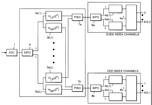
Referring to Figure 5, which is a conceptual representation of the first form
of digital
signal processing apparatus in accordance with the invention, it turns out
that the block
high pass filter and block low pass digital filter of Figure 2 can be replaced
by individual
low 3a(1-L) and high pass 3b(1-L) filters in parallel branches which are fed
cyclically
CA 02214869 1997-09-08
11 P/60887.CAP/NINIS
with samples (SIPO 6) and from which the processed samples are cyclically
combined
(PISO 7a, 7b).
There is no decimation in the low pass and high pass FIR filters 3 of Figure
2. For each
input sample, a complete convolution is carned out and a single output sample
is
generated for input to unit 4a and another generated for input to unit 4b.
When the same samples are input to SIPO 6 in Figure 5, the same output samples
are fed
to SIPO 8a and SIPO 8b as would have been generated by the block fine filter 3
of
Figure 2.
A simple example with reference to Figures 7a, 7b, 8a, 8b, 9a, 9b will show
why this is
so.
For simplicity only demultiplexing operations are described in detail but all
functions
work equally well in reverse.
The imaged tight filter function 3 is used to pre-process data prior to
demultiplexing or
post-process data following multiplexing. The design is based around a
prototype low
pass filter which would be suitable for extracting a single slot centred at DC
from an
FDM of two slots as shown in Figure 7a.
This is a half band filter as it is symmetric about the normalised frequency
position of
~/2. This also means that the filter is contiguous.
CA 02214869 1997-09-08
12 P/60887.CAP/NiNIS
The characteristics of the filter coefficients for such a half band filter are
shown in
Figure 7b. Hence the filter taps are also symmetric with alternate zero taps
except for
a large centre tap. The filter length is commonly described in terms of the
parameter J
which is the number of distinct taps excluding the centre tap. Hence, the
overall filter
length is described by the equation
N = 4J-1
The prototype low pass filter can be simply converted into a high pass filter
as shown in
Figure 8a. The only change to the filter coe~cients is the negation of all the
taps except
the centre tap. The same filter can therefore be used to generate both the low
and high
pass versions of a signal using identical partial products. It is merely the
final
summation that determines which band is generated.
The process of imaging the prototype filter is to insert zeros between the
prototype taps.
For the filter to be imaged M times, M-1 zeros must be inserted. Figure 9a
shows the
low pass filter imaged by a factor of two. This filter is now suitable for
extracting two
slots from an FDM of four and, in general, the imaging factor will be equal to
half the
number of slots within the FDM.
The imaged high pass version can again be derived from the equivalent low pass
version
by subtracting the centre tap instead of adding it. The resultant filter would
now be
suitable for extracting the other two slots from a four slot FDM.
For each input sample, a complete convolution is carried out and a single
output
generated for the low pass filtered version and the high pass filtered
version. The
CA 02214869 1997-09-08
13 P/60887.CAP/NINIS
process of imaging, however, is achieved by inserting zeros between each of
the filter
taps. Each input sample is therefore only multiplied by a non-zero filter tap
at most once
for M input samples.
This can be seen for Figure 9b where the prototype filter is interpolated by a
factor of 2.
A sample entering the filter is multiplied by the first filter tap. It is only
after four more
input samples are loaded before the data is used again, all the taps between
being zero.
When the data reaches the centre of the filter, the frequency of non-zero taps
increases
so that the sample is needed on every other output sample.
As there is a separation of M samples between the times when each sample is
needed,
a contiguous sequence of M data values will never be convolved to form an
output
sample. Each sample within the block can therefore be considered to be
operated upon
by a completely distinct filter. This filter will be the prototype low pass or
high pass by
which the imaged filter was generated.
An alternative structure to using a single imaged tight filter is therefore to
explicitly use
multiple versions of the prototype. Each filter would accept a sub-sampled
version of
the input sequence and the output from each would correspond to a sub-sampled
version
of the output if a single imaged device had been used. This arrangement is
shown in
Figure 10 and gives the maximum parallelisation possible using an imaged tight
filter.
Thus M branches are used where M is equal to half the number of slots within
the FDM
to be demultiplexed.
CA 02214869 1997-09-08
14 P/60887.CAPMINIS
Complete parallelism is not necessary for the imaged tight filter. It could
for example
be split into only M/2 branches, each branch performing an imaged filter based
on only
a four channel FDM. The conditions on splitting the fully imaged version are
given by
equation 2.1:
M = nL (2.1 )
where n is an integer.
Irrespective of the level of parallelism chosen for the imaged filtering
operation, the total
number of multiplication and addition operations remain the same. Each device
within
a chain, however, will require its own copy of the filter coefficients
although this number
is relatively small.
Reference is again made to Figure 5, which shows a conceptual representation
of the first
form of digital signal processing apparatus for frequency demultiplexing a
wideband
channel into K-sub-bands.
Thus, ADC 1 feeds a serial-to-parallel converter 6. The first sample from ADC
1 goes
to branch 1, the second to branch 2, the Lth to branch L, and the L+lth to
branch 1. The
first digital filter 3 is implemented as pairs of filters 3a(1), 3b(1) to
3a(L), 3b(L). The
parts 3a correspond to the output 3 of Figure 2 which produced the low pass
response
of Figure 3a, and the parts 3b correspond to the output 3 of Figure 2 which
produced the
high pass response of Figure 3f The low pass outputs are converted into a
serial data
stream in parallel-to-serial converter 7a, and likewise the high pass outputs
in parallel-to-
serial converter 7b (corresponding to the outputs of the first digital filter
3 which pass
CA 02214869 1997-09-08
15 P/60887.CAP/M1VIS
to 4a and 4b respectively).
In turn, second digital filter 4a, 4b are each implemented by processors 4a(1)
to 4a(L)
and 4b(1) to 4b(L) in parallel branches, fed by serial-to-parallel converters
8a, 8b.
In the second form of digital signal processing apparatus of Figure 6,
converters 7a, 8a,
7b, 8b are omitted, and it has surprisingly been found that 3a(1) can be
connected
directly to 4a(1), 3b(1) to 4b(1) etc. This will be discussed in more detail
below.
In the case of both digital signal processing apparatuses, it is possible to
implement the
second digital filter using processors in parallel branches by executing the
FFTs as
partial FFTs in an FFT decomposition. It is possible to implement the first
digital filter
in parallel branches in both apparatuses for reasons explained.
The parallel implementation of the first form demultiplexer will now be
explained in
greater detail. The first digital filter 3 of Figure 2 is a single rate
structure with no
decimation or interpolation between the input and output sampling rates. The
unit
sample response of the digital filter 3 is that of a prototype FIR filter (a
I/2-band design)
with an additional L-1 zeros padded between each coefficient, L being the
interpolation
factor between the sampling rate of the prototype 1/2-band filter and the
sampling rate
of the input. With the real input signal being divided into K equal sub-bands
L = K.
The realisation of the first digital filter 3 as parallel low-rate branches in
this general case
can be understood by considering the polyphase decomposition of the input
signal, as
CA 02214869 1997-09-08
16 P/60887.CAP/M1VIS
shown in Figure 11 a. Each output sample from the first digital filter 3 of
Figure 2 is the
sum of L branch computations, L-1 of which are identically zero on any output
sample
due to the zero-padded nature of the unit sample response. The summation can
be
replaced with a commutator and the input signal also delivered to each branch
with a
commutator, as shown in Figure 11b. The first digital filter can therefore be
implemented as a set of up to L parallel low sampling rate branches with input
and
output commutators as shown in Figure 11 c; in the case where the maximum of L
branches are used n = 1 and each branch filter is simply a copy of the
original 1/2-band
prototype filter.
Each of the two full rate outputs from the first digital filter is processed
in a second
digital filter. The second digital filter applies a 2K-point FFT on successive
windowed,
abased, segments of its input which are prepared by the WOLA filter. The
windowed
segments could be of length N = 6K, overlapped by K samples (the output
decimation
factor), and abased by 3 to form the 2K sample segment input to the FFT.
There are L <_ K branches in the first digital filter and if the second
digital filter is also
realised as L independent branch structures then the two sets of branches can
be
combined as a set of L separate parallel processing chains, as shown in Figure
4.
The key to the realisation of the second digital filter in this way is to
exploit the fact that
the 2K-point FFT can be performed as a 2D FFT based on a row-column
decomposition
of the samples with L rows (processors 4a(1) to 4a(L): 4b(1) to 4b(L)) and
(2K/L,)
columns (processors 4a', 4b'), where the placing of samples into the rows is
performed
CA 02214869 1997-09-08
17 P/60887.CAP/NINIS
in natural order using a commutator. The WOLA filter function can be realised
as L
separate branch processes (see Figure 6) provided that the overall decimation
factor in
the second digital filter, M, and the number of branches L satisfy the
relation:
M = nL, where n is an integer >_ 1.
In the architectures of Figures 5 and 6, the second digital filter decimation
factor M = K,
and the number of branches L <_ K, so the above equation is satisfied. The
architectures
with output decimation by K can therefore be implemented in parallel form with
L = K/n
branches.
The WOLA filter could have a unit sample response of length Nae~~,a a;~~ s~t~
= 6K, which
is applied as a multiplicative windowing function to the signal samples prior
to the
2K-point FFT. In the parallel implementation of each second digital filter
into L = K/n
branches, based on a decomposition of the 2K-point FFT into (K/n) 2n-point row
FFTs
and 2n (K/n)-point column FFTs, the length of the segment of window in each
branch
is 6n. The multiplication and aliasing operation in each branch is performed
as a set of
2n FIR-type convolutions generating the 2n inputs to the row FFTs.
Only a partial transform is required on each of the two second digital
filters, since each
produces half the demultiplexed slots (and in turn half of these are not
computed since
they are complex conjugates). This means that a total of Zn column FFT
processors (4a',
4b') are required to complete the demultiplexing of the K channel slots, the
column FFT
being a (K/n)-point transform. The 2n-point row transforms can also be
implemented
CA 02214869 1997-09-08
18 P/60887. CAP/1VFVIS
as partial FFTs because only half of the outputs from any given branch FFT are
required.
In general the 2D decomposition uses the Cooley-Tukey algorithm, which
requires an
intermediate set of twiddles between the 2n-point row FFTs and the (K/n)-point
column
FFTs. Because each second digital filter performs a partial FFT, only about
half the
twiddles are required on each.
Figure 6 shows the generic form of the parallel architecture for the high
speed front-end
demultiplexer which divides the input FDM into K sub-bands. The ADC 1 delivers
a
real sample sequence at rate fg with wordlength b. This is converted to L =
K/n parallel
streams each at rate nfs /K which are processed as shown in the branch chains.
The
branch processors are identical apart from the 6n (in this example) distinct
coefficients
in each partial WOLA. The branch inputs are real, and the outputs are in
general
complex. The demultiplexing is completed with the set of 2n complex-complex
(K/n)-
point column FFTs (4a', 4b'), each of which synthesises K/2n useful outputs.
In the implementation shown in Figure 6, the twiddles W~ are shown acting on
the
inputs to the column FFT processors. In practice, implementation
considerations would
probably dictate that the twiddles are implemented on the branch processors to
avoid
excessive complexity in the column FFT processor. The input FDM could comprise
8
channel slots on a 42 MHz spacing, in an even stacking configuration. To
extract 6
useful slots spanning 252 MHz it is necessary that the passband of the
analogue filter
providing the input to the ADC 2 spans 7 slots with a bandwidth of 294 MHz;
the shape
factor of the AAF is therefore 9/7 and the sampling frequency is 672 Msps.
CA 02214869 1997-09-08
19 P/60887. CAP/N>1VIS
The Tables below show how certain key parameters vary as a function of K, the
number
of sub-bands, for two possible architecture options.
Cooley-Tukey decomposition, n = 1
parameterdescription K--8 K=16 K--32 K--64
fs input sampling rate672 672 672 672
Msps
L number of branch 8 16 32 64
chains
fs/L branch input sampling84 42 21 10.5
rate
fs/K branch output sampling84 42 21 10.5
rate
K1 column FFT size 8 16 32 64
sub-bands/channel 1 2 4 8
Cooley-Tukey decomposition, n = 2
parameterdescription K--8 K=16 K--32 K~4
fs input sampling rate672 672 672 672
Msps
L number of branch 4 8 16 32
chains
fs/L branch input sampling164 84 42 21
rate
fs/K branch output sampling84 42 21 10.5
rate
K1 column FFT size 4 8 16 32
sub-bands/channel 1 2 4 8
Twiddles between the row FFTs and the column FFTs can be eliminated if a Good-
Thomas decomposition is used; this however imposes certain constraints on the
architecture.
The parameters which characterise a parallel implementation of the
architecture are
summarised in the Table below.
CA 02214869 1997-09-08
20 P/60887. CAP/1VPVIS
parameter description
fs sampled bandwidth of real input is fs/2
b ADC sample wordlength
K number of sub-band slots
n,m integers > 0
i
K/n number of branch chains
nfs/K sampling rate of branch chain input (real)
fs/K sampling rate of branch chain outputs
(complex)
2nm number of column FFT processors
K/nm size of com lex-com lex column FFT
The lowest complexity branch processor option is n = 1 and m = 1. However
there are
disadvantages with opting for this minimum complexity branch processor. The
number
of chains is maximised at L = K which could complicate the layout of the
demultiplexer
subsystem, and it also implies that the column FFT size is maximised at K.
A better balance between branch and column processor complexity is achieved by
taking
n = 2. This halves the number of processing chains required and also halves
the column
FFT size to K/2 (although twice as many are required).
There remains the difficulty that with m = 1 the only option is to use the
Cooley-Tukey
decomposition of the FFT, which adds a significant complexity to the branch
processors
which each have to have a complement of "twiddle" factors.
It is considered that the optimum partitioning is to use a Good-Thomas
decomposition
with n = 2 and m = 2. This results in a branch processor of intermediate
complexity and
CA 02214869 1997-09-08
21 P/60887.CAP/MNIS
the column FFT size is halved again to K/4.
The sample deinterleaver (serial-to-parallel converter)and interleaver
(parallel-to-serial
converter) functions are relatively simple to implement using flip-flops. The
ADC will
have 2 output channels, at 8 bits each. Each channel is divided into 7
separate sample
streams with 14 flip-flops/bit, giving a total 1-14 deinterleaver. The
complete unit
therefore requires 224 flip-flops, each drawing 3.05 mW to give a total of 683
mW.
Adding I/O the total power for the 1-14 SIPO unit in GaAs would be less than 5
W.
The arrangements of Figures 5 and 6 may have a useful bandwidth of 252
MHz, comprising six 36 MHz channels on a 42 MHz channel centre spacing. The
Good-
Thomas algorithms may be used to provide 23 useful 9 MHz sub-bands spanning
240
MHz which lie in the positive frequency half of the AAF passband. The sub-
bands are
on a 10.5 MHz spacing and are oversampled by 2 on the output of the
demultiplexer at
21 Msps. Note that by going to a finer granularity the shape factor of the AAF
and AIF
filters can be increased and at the same time the overall sampling rate
reduced by more
than 10% from 672 Msps to 588 Msps. Figure 1 shows such an organisation of the
channel. Clearly, this is much more flexible than existing analogue
arrangements. A
user who only needed a small bandwidth, say, 9 MHz, would not be constrained
by the
analogue implementation, into purchasing the use of far more bandwidth (36
MHz minimum), than required, thereby saving cost.
In either bandwidth organisation, the parallel implementation permits the use
of
processors in the parallel branches operating at no more than 42 Msps, so that
cheaper
CA 02214869 1997-09-08
22 P/60887.CAP/NINIS
CMOS processors e.g. on ASICs can be used, whereas if an attempt was made to
implement the embodiments in the serial form of Figure 2, data processing
speeds of at
least 588 Msps would be required, which would not be practicable to implement
in
today's technology even if expensive GaAs processors were used.
Multiplexers according to the invention work in an inverse manner to the
demultiplexers
described with the caveat that in the multiplexer mode the first digital
filter is bypassed
if the baseband inputs are oversampled by 2.
The processing apparatus is suitable for transparent as well as regenerative
satellites.
Of course, variations may be made without departing from the scope of the
invention.
Thus, while the embodiments of Figures 5 and 6 have been described in relation
to a
wide bandwidth channel, that is wide compared to the 4 MHz typical bandwidth
of the
prior art Figure 2 arrangement, the invention is also applicable to such
narrow bands, and
is even applicable to wider bands than those referred to above, for example,
to a band of
588 MHz, or to bandwidths between 4 MHz and 588 Mhz. Further, further
(de)multiplexing of the kind described in EP-A-0 695 054 may be performed on
each
sub-band in the above described embodiment.