Note: Descriptions are shown in the official language in which they were submitted.
CA 02214982 1997-09-11
SEI 96--36
DESCRIPTION
OPTICAL WAVEGUIDE MODULE
Technical Field
The present invention relates to an optical waveguide
module which encapsulates an optical waveguide device
utilized for branching, coupling, or the like of signal
light in an optical transmission system. More
particularly, the invention concerns the package
structure of the optical waveguide module applicable to
fiber-optic communication systems requiring high
reliability.
Background Art
The conventional optical waveguide modules are
arranged to comprise an optical waveguide device, which
is utilized for branching, coupling, or the like of
signal light, for optically interconnecting optical
fibers being transmission lines, and a case for
enclosing the optical waveguide device therein.
Further, a space between the case and the optical
waveguide device is filled with a buffer protector.
The buffer protector functions to absorb impact or the
like exerted from the outside of the case on joint
portions and the like between an optical waveguide
incorporated in the optical waveguide device and
optical fibers.
Here, the above optical waveguide device comprises
-
CA 02214982 1997-09-11
SEI 96-36
a waveguide substrate having an optical waveguide
provided in its upper surface and having the function
of branching, coupling, etc. of signal light, a silicon
V-grooved support member (first support member) for
optically connecting one end of the optical waveguide
with one end of an input optical fiber, attached to the
tip of the input optical fiber, and a silicon V-grooved
support member (second support member) for optically
connecting the other end of the optical waveguide with
one end of an output optical fiber, attached to the tip
of the output optical fiber. The first and second
support members are fixed to the both end faces of the
waveguide substrate with the optical waveguide being
axially aligned with the input and output optical
fibers (or in an optically interconnected state).
The structure of optical waveguide module as
described above is disclosed, for example, in Japanese
Laid-open Patent Application No. 5-27139.
Disclosure o~ Invention
The present invention concerns the package
structure of the optical waveguide module applicable to
fiber-optic communication systems requiring high
reliability. The inventors investigated the
conventional optical waveguide module as described
above and found that the conventional optical waveguide
module cannot sufficiently prevent occurrence of
CA 02214982 1997-09-11
SEI 96-36
expansion and contraction of the case with change of
ambient temperature.
Namely, the input optical fiber and output optical
fiber are subject to tensile stress under high-
temperature environment or subject to shear stress
under low-temperature environment, depending upon their
setting environment. This results in deteriorating
adhesive strength of an adhesive bonding the V-grooved
support member to the waveguide substrate with a lapse
of time, which will increase optical losses due to
axial shift at the joint surfaces between these
members. Further, if deterioration of adhesive
strength of the adhesive is great, the V-grooved
support member can be peeled off from the waveguide
substrate.
A conceivable countermeasure is to change the
material for the case to glass or liquid crystal
polymer with a low coefficient of linear thermal
expansion, but in this case, glass has such a strength
property that it is weak against impact, while the
liquid crystal polymer has such a processing property
that it is not easy to make a thin case thereof.
There~ore, they cannot achieve downsizing of the case
as a result.
It is also conceivable to preliminarily give the
input optical fiber and output optical fiber a marginal
-
CA 02214982 1997-09-11
SEI 96-36
length and encapsulate them in a curved state inside
the case. However, the encapsulating work of these
optical fibers requires too much labor and time, which
is not suitable for mass production.
It is, therefore, an object of the present
invention to provide an optical waveguide module
excellent in environmental resistance characteristics
and high in reliability, which can reduce the number of
components of a package for housing the optical
waveguide device and which has the package structure
capable of protecting the optical waveguide device
against stress due to the change of ambient temperature
or against impact or the like acting from the outside.
In order to achieve the above object, an optical
waveguide module according to the present invention
comprises, for example as shown in Figs. 2 - 7, an
optical waveguide device 30 as an optical functional
device having the function of branching, coupling, or
the like of signal light, for optically interconnecting
optical fibers, a first reinforcing member 110 (a metal
plate member) constituting at least a part of a case
housing the optical waveguide device 30, and a buffer
protector 400 covering at least the optical waveguide
device 30 and parts of the optical fibers and adhering
to the first reinforcing member 110 in predetermined
strength.
:
CA 02214982 1997-09-11
SEI 96-36
The optical waveguide device 30 has a waveguide
substrate 32 in an upper surface 321 of which an
optical waveguide 320 is provided, a first support
member 31 attached to the tip of input optical fiber
340 and fixed to one end face of the waveguide
substrate 32 in such a state that one end of the
optical waveguide 320 is optically connected to one end
of the input optical fiber 340, and a second support
member 33 attached to the tip of output optical fiber
360 and fixed to the other end face of the waveguide
substrate 32 in such a state that the other end of the
optical waveguide 320 is optically connected to one end
of the output optical fiber 360 (see Fig. 1). An
optical fiber comprises a core having a predetermined
index of refraction and a cladding provided around the
periphery of the core and having an index of refraction
lower than that of the core.
The first reinforcing member 110 is a metal plate
having a reference surface 111 facing the waveguide
substrate 32 and shaped so as to be open at least in
the longitudinal direction of the optical waveguide
device 30, which has edge portions 170, 171 (first and
second edge portions) as bent so as to face each other.
In addition, at least a part of the optical waveguide
device 30 is housed in a space defined by the reference
surface 111, a surface 112 of the edge portion 170
CA 022l4982 l997-09-ll
SEI 96--36
continuous from the reference surface 111, and a
surface 113 of the edge portion 171 continuous from the
reference surface 111.
The buffer protector 400 adheres to at least the
reference surface 111 of the first reinforcing member
110 in the predetermined strength and has such adhesive
strength that the product of the adhesive strength and
an adhesion area on the reference surface 111 of the
first reinforcing member 110 in contact with the buffer
protector 400 is 0.5 or more kgf (Bellcore standard)~
Particularly, preferable materials for the,buffer
protector 400 have the modulus of elasticity in the
range of 1 kgf/cm2 to 20 kgf/cm2 after curing.
The buffer protector 400 is relatively soft because
of possession of the modulus of elasticity in the range
of 1 kgf/cm2 to 20 kgf/cm2 after curing. Because of it,
even if the case is subject to thermal expansion or
thermal contraction with change of ambient temperature,
thermal stress acting on the optical waveguide device
30 can be suppressed by intervention of the buffer
protector 400.
The buffer protector 400 can be filled uniformly
between the case and the optical waveguide device 3 0 by
capillarity, immediately flowing it into the case.
Therefore, no gap remains between the case and the
optical waveguide device 30, So that no thermal stress
CA 02214982 1997-09-11
SEI 96-36
will occur from the inside of the buffer protector 400.
Further, since the buffer protector 400 has the
relatively low modulus elasticity and the case (metal
plate) has relatively high strength, mechanical impact
acting on the optical waveguide device 30 from the
outside of the case is buffered through the buffer
protector 400 and the case. These stably fix and
position the optical waveguide device 30 even with
occurrence of change of ambient temperature or even
with action of external impact thereon. In addition,
the above arrangement can reduce the temporal change of
adhesive strength of the adhesive adhering the first
support member 31, waveguide substrate 32, and second
support member 33 to each other.
Therefore, the well-aligned state can be maintained
at each of the first joint part between the input
optical fiber 340 and the optical waveguide 321 and the
second joint part between the optical waveguide 321 and
the output optical fiber 360. In addition, losses of
optical signal transmitted from the input optical fiber
to the output optical fiber can be suppressed stably
with a lapse of time.
Further, the optical waveguide module according to
the present invention comprises a first edge component
210 (150) having a through hole 211 (151) for letting
the input optical fiber 340 pass and an adhesion
CA 02214982 1997-09-11
SEI 96-36
surface 212 (153) to be bonded to the buffer protector
400, and a second edge component 220 (160) having a
through hole 221 (161) for letting the output optical
fiber 360 pass and an adhesion surface 222 (163) to be
bonded to the buffer protector 400. In this way, these
first and second edge components 210, 220 close the
open areas in the longitudinal direction of the optical
waveguide device 30.
Further, the optical waveguide module according to
the present invention may be arranged in such a way
that the buffer protector 400 is provided in the space
defined by the reference surface 111 of the first
reinforcing member 110, the surface 112 of the edge
part 170 continuous from the reference surface 111, and
the surface 113 of the edge part 171 continuous from
the reference surface 111 in such a state as to cover
the whole of the optical waveguide device 30 and that
the buffer protector also covers the whole of the first
reinforcing member 110 (see Figs. 11 and 12).
Further, the case housing the first optical
waveguide device 30 may be comprised of the foregoing
first reinforcing member 110 and a second reinforcing
member 120 having a reference surface 121 facing the
waveguide substrate 32 and shaped so as to be open at
least in the longitudinal direction of the optical
waveguide device 30. Particularly, this second
CA 02214982 1997-09-11
SEI 96-36
reinforcing member 120 also has edge portions 180, 181
(third and fourth edge parts) bent so as to face each
other. The second reinforcing member 120 is positioned
so that the reference surface 121 thereof faces the
reference surface 111 of the first reinforcing member
110 with the optical waveguide device 30 inbetween (see
Fig. 16). At this time, the second reinforcing member
120 engages with the first reinforcing member 110 with
the edge portions thereof 180, 181 holding the edge
portions 170, 171 of the first reinforcing member 30.
When the case is comprised of the first and second
reinforcing members 110, 120 in this way, the buffer
protector 400 can also be arranged to cover the whole
of the first reinforcing member 110 and the whole of
the second reinforcing member 120 as covering the whole
of the optical waveguide device 30.
Brief Description of DrawingS
Fig. 1 is an assembly step diagram for explaining
the structure of the optical waveguide device mounted
in the optical waveguide module accordinq to the
present invention;
Fig. 2 is a plain view of the optical waveguide
device mounted in the optical waveguide module
according to the present invention;
Fig. 3 is a drawing to show a first assembly step
for fabricating the first embodiment of the optical
CA 02214982 1997-09-11
,
SEI 96-36
waveguide module according to the present invention;
Fig. 4 is a drawing for explaining a modification
(using alternative members) of the first assembly step
shown in Fig. 3;
Fig. 5 is a drawing to show a second assembly step
for fabricating the first embodiment of the optical
waveguide module according to the present invention;
Fig. 6 is a perspective view of the first
embodiment of the optical waveguide module according to
the present invention, obtained through the assembly
steps shown in Figs. 3 and 5;
Fig. 7 is a drawing to show the cross-sectional
structure of the first embodiment of the optical
waveguide module according to the present invention,
taken along line I-I in Fig. 6;
Fig. 8 is a perspective view to show an application
of the first embodiment of the optical waveguide module
shown in Fig. 6;
Fig. 9 is a drawing to show the first step for
fabricating the second embodiment of the optical
waveguide module according to the present invention;
Fig. 10 is a drawing to show the second step for
fabricating the second embodiment of the optical
waveguide module according to the present invention;
Fig. 11 is a perspective view of the second
embodiment of the optical waveguide module according to
CA 02214982 1997-09-11
SEI 96-36
the present invention, obtained through the assembly
steps shown in Figs. 9 and 10;
Fig. 12 is a drawing to show the cross-sectional
structure of the second embodiment of the optical
waveguide module according to the present invention,
taken along line II-II in Fig. 11;
Fig. 13 is a graph to show the relationship between
ambient temperature applied to the optical waveguide
module and time change, obtained as results of
experiments for checking optical loss variation due to
thermal loads, for the second embodiment of the optical
waveguide module according to the present invention
shown in Figs. 11 and 12;
Fig. 14 is a graph to show the relationship between
modulus of elasticity of the buffer pr~otector and
optical loss variation, obtained as results of
experiments for checking the optical loss variation due
to thermal loads, for the second embodiment of the
optical waveguide module according to the present
invention shown in Figs. 11 and 12;
Fig. 15 is a graph to show the relationship between
modulus of elasticity of the buffer protector and
optical loss variation, obtained as results of
experiments for checking the optical loss variation due
to external force loads, for the second embodiment of
the optical waveguide module according to the present
-
CA 022l4982 l997-09-ll
SEI 9 6--3 6
invention shown in Figs. 11 and 12;
Fig. 16 iS a drawing to show a part of assembly
step for fabricating the third embodiment of the
optical waveguide module according to the present
invention;
Fig. 17 is a perspective view to show the third
embodiment of the optical waveguide module according to
the present invention, obtained through the assembly
step shown in Fig. 16;
Fig. 18 is a drawing to show the cross-sectional
structure of the third embodiment of the optical
waveguide module according to the present invention,
taken along line III-III in Fig. 17;
Fig. 19 is a drawing to show the cross-sectional
structure of the ~ourth embodiment of the optical
waveguide module according to the present invention;
Fig. 20 is a perspective view to show an
application of the third embodiment of the optical
waveguide module shown in Fig. 17; and
Fig. 21 is a drawing to explain a method di~fer to
the fabricating method shown in Figs. 9 and 10, for
~abricating the fourth embodiment of the optical
waveguide module shown in Fig. 19.
Best Mode for Carrying Out the Invention
The structure of each embodiment of the optical
waveguide module according to ~he present invention
12
CA 02214982 1997-09-11
SEI 96-36
will be described with reference to Fig. 1 to Fig. 21.
The same elements in the drawings will be denoted by
the same reference numerals and redundant description
will be omitted. It is also noted that the dimensional
ratios of the drawings are not always coincident with
those in the description.
Fig. 1 is an assembly step diagram for explaining
the structure of the optical waveguide device mounted
in the optical waveguide module according to the
present invention. As shown in this figure, the
optical waveguide device 30 comprises a fiber support
31 (first support member) attached to the tip of input
optical fiber 340 for transmitting signal light and
fixed to the tip, a waveguide substrate 32 in an upper
surface 321 of which an optical waveguide 320 for
branching or coupling the signal light incident to its
input end from the input optical fiber 340 to guide the
signal light to its output end is provided, and a fiber
support 33 (second support member) attached to the tip
of output optical fibers 360 for guiding the signal
light emerging from the output end of the optical
waveguide 320 and fixed to the tip. In addition, these
fiber supports 31, 33 are bonded to either end face of
the waveguide substrate 32 with a first adhesive 37.
The fiber support 31 comprises a silicon lower
member 311 for supporting the single-core input optical
CA 02214982 1997-09-11
SEI 96-36
fiber 340 in its single V-shaped groove formed in its
surface, and an upper member 310 of transparent glass
adhered, together with the lower member 311, to the
input optical fiber 340 with a second adhesive 38 and
bonded onto the surface of the lower member 311 with
the second adhesive 38. The back surface of this upper
member 310 urges the input optical fiber 340 against
the lower member 311. Here, the exit-side end face of
the input optical fiber 340 is exposed while being
aligned with the exit-side end face of the fiber
support 31. The surface of the input optical fiber 340
is coated with a plastic coating except for the tip
portion, and in the figure numeral 34 denotes a fiber
cable including the input optical fiber 340.
On the other hand, the fiber support 33 also
comprises a silicon lower member 331 for supporting 8-
core output optical fibers 360 in eight corresponding
V-shaped grooves formed in its surface, and an upper
member 330 of transparent glass adhered, together with
the lower member 331, to the output optical fibers 360
with the second adhesive 38 and bonded onto the surface
of the lower member 331 with the second adhesive 38.
The back face of this upper member 330 urges the output
optical fibers 360 against the lower member 331. Here,
the entrance-side end faces of the output optical
fibers 360 are exposed while being aligned with the
14
-
CA 022l4ss2 Iss7-os-ll
SEI 96-36
entrance-side end face of the fiber support 33. The
surfaces of the respective output optical fibers 360
are covered integrally with a plastic coating except
for their tip portions, and in the figure numeral 36
denotes a tape-type fiber cable (ribbon fiber)
including these output optical fibers 360.
The waveguide substrate 32 is a glass member, in
the surface of which 8-branched optical waveguide 320
of l-input and 8-output type is formed by the normal
flame hydrolysis deposition process. The waveguide
substrate 32 may be a member made of silicon. Here,
the entrance-side end face and exit-side end faces of
the optical waveguide 320 are exposed while being
aligned with the entrance-side end face and exit-side
end ~ace, respectively, of the waveguide substrate 32.
The first joint part between the exit-side end face
of the fiber support 31 and the entrance-side end face
of the waveguide substrate 32 is fixed with the first
adhesive 37 while the exit-side end face of the input
optical fiber 340 is axially aligned with the entrance-
side end face of the optical waveguide 320. On the
other hand, the second joint part between the exit-side
end face of the waveguide substrate 32 and the
. entrance-side end face of the fiber support 33 is fixed
with the first adhesive 37 while the exit-side end
faces of the optical waveguide 320 are axially aligned
CA 02214982 1997-09-11
,
SEI 96-36
with the entrance-side end faces of the output optical
fibers 360 (see Fig. 2).
Here, the first and second adhesives 37, 38 are
ultraviolet (UV) curable adhesives. The first adhesive
37 is a material which has a refractive index matching
with at least those of the core area of the input
optical fiber 340, the optical waveguide 320, and the
core area of the output optical fibers 360 and which is
transparent to the signal light propagating therein.
The second adhesive may be either one selected from
thermosetting adhesives and composite adhesives
containing an ultraviolet curable catalyst and a
thermosetting catalyst, as well as the ultraviolet
curable adhesives.
In particular, preferable materials for the upper
member 310 and 330 can be selected form, for example,
silicon, silica glass (transparent glass as described
above, it is useful because W light can be transmitted
therethrough), ceramic, or the like. Preferable
materials for the lower member 311 and 331 can be
selected from, for example, silicon (V-shaped grooves
can be easily formed therein), silica glass
(transparent glass as described above, it is useful
because W light can be transmitted therethrough),
ceramic (zirconia, crystal quartz), or the like.
Further, preferable materials for the waveguide
16
CA 02214982 1997-09-11
SEI 96-36
substrate 32 can be selected from, for example,
silicon, silica glass, or the like. When both the
upper member 310 and the lower member 311 are made of
epoxy resin containing filler of 80 % or more, the
fiber support 31 can be integrally-molded. Also, when
both the upper member 330 and 331 are made of epoxy
resin containing filler of 80 % or more, the fiber
support 33 can be integrally-molded similarly.
First Embodiment
The first embodiment of the optical waveguide
module according to the present invention will be
described next with reference to Fig. 3 to Fig. 7.
As shown in Fig. 3, the optical waveguide module of
the first embodiment comprises a first reinforcing
member 110 (a metal plate member) constituting at least
a part of the case for housing the optical waveguide
device 30. This first reinforcing member 110 is a
metal plate having a reference surface 111 and shaped
so as to be open at least in the longitudinal direction
of the optical waveguide device 30, which has edge
portions 170, 171 as bent in the directions indicated
by arrows S2, S1, respectively, in the drawing, so as
to ~ace each other. The optical waveguide device 30 is
set in a space defined by the reference surface 111, a
surface 112 of the edge portion 170 continuous from the
reference surface 111, and a surface 113 of the edge
CA 02214982 1997-09-11
SEI 96-36
portion 171 continuous from the reference surface 111
with an upper surface 321 thereof (which is the surface
where the optical waveguide 320 is provided) being
faced to the reference surface 111 of the first
reinforcing member 110. The first reinforcing member
110 and the optical waveguide device 30 may be arranged
such that a lower surface 322 opposed to the upper
surface 321 and the reference surface 111 face each
other.
Further, a first edge component 210 (rubber boot)
having a through hole 211 through which the fiber cable
including the input optical fiber 340 passes and having
an adhesion surface 212 is provided in one open area of
the first reinforcing member 110 in the longitudinal
direction of the optical waveguide device 30. On the
other hand, a second edge component 220 (rubber boot)
having a through hole 221 through which the fiber cable
including the output optical fibers 360 passes and an
adhesion surface 222 is provided in the other open area
of the first reinforcing member 110 in the longitudinal
direction of the optical waveguide device 30. The
optical waveguide device 30 is set in the space defined
by these surfaces 111, 112, 113, 211, 222.
Although the above first and second edge components
210, 220 are components made of rubber, they may be
metal plate members 150, 160 having a through hole 151,
18
CA 022l4ss2 Isg7-og-ll
SEI 96-36
161, respectively, as shown in Fig. 4. Further, if
these plate members 150, 160 are provided with cut
portions 152, 162, the fabrication steps can be
simplified more. In the case of this structure, the
optical waveguide device 30 is also set in the space
defined by these surfaces 111, 112, 113, 153, 163.
Subsequently, as shown in Fig. 5, the buffer
protector 400 is poured into the space as the optical
waveguide device 30 is set in the space defined by the
surfaces 111, 112, 113, 212, 222. While this buffer
protector 400 is poured, predetermined tension is
exerted on each fiber cable 34, 36 in the direction
indicated by an arrow S3 or S4, respectively, in the
drawing. Namely, by pulling the cables 34, 36 in the
directions indicated by S3, S4, the optical waveguide
device 30 is installed at a predetermined position in
the space filled with the buffer protector 400.
The optical waveguide module (the first embodiment)
according to the present invention is attained through
the above steps. Fig. 6 is a perspective view of the
first embodiment of the optical waveguide module
according to the present invention and Fig. 7 is a
drawing to show the cross-sectional structure of the
first embodiment of the optical waveguide module
according to the present invention, taken along line I-
I in Fig. 6.
19
CA 02214982 1997-09-11
SEI 96-36
As shown in Figs. 6 and 7, in the optical waveguide
module of the first embodiment the buffer protector 400
is exposed from the upper opening of the first
reinforcing member 110 constituting the case.
The buffer protector 400 is of urethane rubber and
has the modulus of elasticity in the range of about 1
kgf/cm2 to about 20 kgf/cm2 after curing. In
particular, actually employed was MU-102 available from
Nippon Pelnox Corporation. This buffer protector 400
covers the whole of the optical waveguide device 30 set
inside of the first reinforcing member 110. In
addition, the buffer protector 400 adheres at least to
the reference surface 111 of the first reinforcing
member 110 in predetermined strength and has such
adhesive strength that the product of the adhesive
strength and the adhesion area on the reference surface
111 of the first reinforcing member 110 in contact with
the buffer protector 400 is 0.5 or more kgf (Bellcore
standard). Further, the first reinforcing member 110
is of stainless steel which is a metal member having
high strength, for example, SUS 304.
Here, the buffer protector 400 is relatively soft
because it has the low modulus of elasticity in the
range of about 1 kgf/cm2 to about 20 kgf/cm2 after
curing. Because of it, even if the first reinforcing
member 110 is subject to thermal expansion or thermal
CA 02214982 1997-09-11
SEI 96-36
contraction with change of ambient temperature, the
thermal stress acting on the optical waveguide device
30 is suppressed by intervention of the buffer
protector 400.
The buffer protector 400 can intrude uniformly into
the space between the first reinforcing member 110 and
the optical waveguide device 30 by capillarity,
immediately flowing it into the case. Therefore, there
remains no gap between the first reinforcing member 110
and the optical waveguide device 30, so that no thermal
stress occurs from the inside of the buffer protector
400.
Further, since the buffer protector 400 has the
relatively low modulus of elasticity and the first
reinforcing member 110 (the case) has the relatively
high strength, the mechanical impact acting along
predetermined directions from the outside to the
optical waveguide device 30 is buffered through the
buffer protector 400 and first reinforcing member 110.
As explained above, even with occurrence of change
of ambient temperature or even with action of external
impact, the optical waveguide device 30 is fixedly
positioned stably in the case, and the temporal change
of adhesive strength of the first adhesive 38 for
adhesion at the joint part between the fiber support 31
and the waveguide substrate 32 and at the joint part
21
CA 02214982 1997-09-11
SEI 96-36
between the waveguide substrate 32 and the fiber
support 33 decreases. In addition, the well-aligned
state can be maintained at the first joint part between
the input optical fiber 340 and the optical waveguide
320 and at the second joint part between the optical
waveguide 320 and the output optical fibers 360.
Further, the transmission losses of signal light
transmitted from the input optical fiber 340 to the
output optical fibers 360 are supprèssed stably with a
lapse of time.
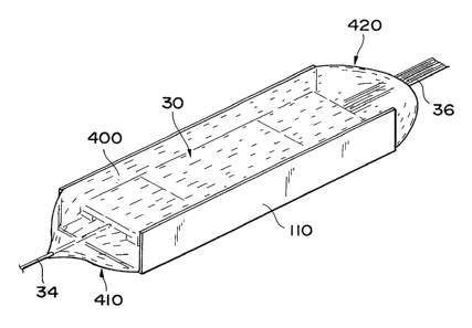
Further, as shown in Fig. 8, portions (edge
portions 410 and 420 of the buffer protector 400) may
lie off the first reinforcing member 110. Fig. 8 is a
perspective view to show an application of the first
embodiment tFlg. 6) of the optical waveguide module
according to the present invention.
In this application, the edge components 210 and
220 in Fig. 6 are unnecessary. Additionally, the edge
portions 410 and 420 of the buffer protector 400
function to prevent the break of the fiber cables 34
and 36.
Second Embodiment
Further, an optical waveguide module according to
the present invention may be constructed in such
structure as to cover the whole of the first
reinforcing member 110 (the case) housing the optical
22
CA 02214982 1997-09-11
SEI 96-36
waveguide device 30 with the buffer protector 400.
Fig. 9 and Fig. 10 show fabrication steps of the
optical waveguide module of the second embodiment.
First, as shown in Fig. 9, prepared are lower mold
500 and upper mold 510 each provided with a
predetermined recess. Then the lower mold 500 and
upper mold 510 are coupled with each other so that the
optical waveguide device 30 and the first reinforcing
member 110 are set in a cavity defined by the recesses
of these molds 500, 510 with the optical waveguide
device 30 being set in the first reinforcing member
110. At this time, a release agent is applied to the
surface of each recess of the lower mold 500 and upper
mold 510 and part of the buffer protector 400 is
preliminarily poured into the recess of the lower mold
500.
Subsequently, as shown in Fig. 10, the buffer
protector 400 is poured through a resin inlet port 511
provided in the upper mold 510 into the cavity de~ined
by the recesses of the lower mold 500 and upper mold
510. At this time, predetermined tension is exerted on
each optical fiber 340, 360 in the direction indicated
by an arrow S5 or S6 in the drawing. Namely, the
buffer protector 400 is poured while the cables 34, 36
are pulled in the directions of the arrows S5, S6,
respectively, whereby the optical waveguide device 30
CA 02214982 1997-09-11
SEI 96--36
is set at the predetermined position in the first
reinforcing member 110.
The optical waveguide module (the second
embodiment) according to the present invention is
obtained through the above steps. Fig. 11 is a
perspective view of the second embodiment of the
optical waveguide module according to the present
invention and Fig. 12 is a drawing to show the cross-
sectional structure of the second embodiment of the
optical waveguide module according to the present
invention, taken along line II-II in Fig. 11.
In the optical waveguide module fabricated as
described above, the buffer protector 400 also
functions in the same manner as the buffer protector
400 of the above first embodiment, and as a result, the
optical waveguide module of the present embodiment can
also enjoy substantially the same operational effects
as the optical waveguide module of the first embodiment
described above.
Next described referring to Fig. 13 to Fig. 15 are
results of experiments having been conducted for the
second embodiment by the present inventors.
First, the inventors conducted an experiment to
check the optical loss variation caused by thermal
loads for the second embodiment. In this experiment
six different samples with moduli of elasticity of the
24
CA 02214982 1997-09-11
SEI 96-36
buffer protector 400 included in the range of 0.5
kgf/cm2 to about 100 kgf/cm were prepared as optical
waveguide modules to be compared.
Fig. 13 shows the time change of ambient
temperature loaded on these six types of optical
waveguide modules. In Fig. 13, the abscissa represents
the passing time (h) while the ordinate the ambient
temperature (~C). The highest temperature TH iS +75 ~C,
the lowest temperature TL is -45 ~C, and TR is room
temperature.
Such heat cycle tests with each cycle taking 8
hours were repeated throughout two weeks, and before
and after the tests, the optical loss variation was
measured for the all waveguide devices 30 in each
optical waveguide module prepared. Results of the
measurement are shown in Fig. 14. The measurement of
optical loss is performed by measuring the optical loss
between the input optical fiber 340 and each of the
output optical fibers 3 60, respectively. In this Fig.
14, the abscissa represents the modulus of elasticity
(kgf/cm2) of the buffer protector 400 and the ordinate
the mA~imum optical loss variation (dB) of the optical
waveguide device 30. From Fig. 1 3, after the modulus
of elasticity of the buffer protector 400 exceeds 20
kgf/cm2, the m~;mllm optical loss variation in the
optical waveguide device 30 abruptly increases from
CA 02214982 l99i-09-11
SEI 96-36
below 0.2 dB. Therefore, as long as the modulus of
elasticity of the buffer protector 400 is 20 or less
kgf/cm , the m~X;mum optical loss variation of optical
waveguide device 30 can be suppressed below the level
to raise no problem in practical use, i.e., below 0.2
dB.
Further, the inventors carried out an experiment
for checking the optical loss variation caused by
external loads for the second embodiment. In this
experiment, six different samples with moduli of
elasticity of the buffer protector 400 included in the
range of 0.5 kgf/cm2 to about 100 kgf/cm2 were prepared
as optical waveguide modules to be compared.
These six types of optical waveguide modules were
fixed at the central portion and the tension of 5N,
which was considered to occur in practical use, was
applied to the end portion located on the output
optical fiber 360 side with respect to the central
portion for about one minute. Before and after such
external load tests, the m~x;mum optical loss variation
was measured for the all cores of the optical waveguide
device 30 in each optical waveguide module prepared,
and the results of the measurement are shown in Fig.
15. In this Fig. 15, the abscissa represents the
modulus of elasticity of the buffer protector 400 and
the ordinate the m~;mum optical loss variation of
26
CA 02214982 1997-09-11
.
SEI 96-36
optical waveguide device 30.
From Fig. 15, in the range where the modulus of
elasticity of the buffer protector 400 is smaller than
1 kgf/cm2, the m~;ml~m optical loss variation of optical
waveguide device 30 abruptly increases from below 0.2
dB. Therefore, as long as the modulus of elasticity of
the buffer protector 400 is 1 or more kgf/cmZ~ the
maximum optical loss variation of optical waveguide
device 30 can be suppressed below the level to raise no
problem in practical use, i.e., below 0.2 dB.
Accordingly, the above experiment results confirm
that the optical loss variation of optical waveguide
device 30 can be suppressed below the level to raise no
problem in practical use as long as the modulus of
elasticity of the buffer protector 400 is within the
range of 1 kgf/cm2 to about 20 kgf/cm2.
Third Embodiment
Next, an optical waveguide module according to the
present invention may be comprised of the first
reinforcing member 110 and a second reinforcing member
120 of the same shape and the same material, as a case
for housing the optical waveguide device 30, as shown
in Fig. 16 and Fig. 17.
Particularly, this second reinforcing member 120 is
also made of metal tstainless steel SUS 304)
constituting at least a part of the case for housing
CA 022l4982 l997-09-ll
SEI 96--36
the optical waveguide device 30, similarly as the first
reinforcing member 110 was. Further, this second
reinforcing member 120 is a metal plate having a
reference surface 121 and shaped so as to be open at
S least in the longitudinal direction of the optical
waveguide device 30, which has edge portions 180, 181
(third and fourth edge portions) as bent so as to face
each other. The optical waveguide device 30 is set in
a space defined by the reference surface 121, a surface
122 of the edge portion 180 continuous from the
reference surface 121, and a surface 123 of the edge
portion 181 continuous from the reference surface 121
so that the back face 322 thereof (on the opposite side
to the upper surface 321) is faced to the reference
surface 121 of the second reinforcing member 120.
The optical waveguide module of the third
embodiment is fabricated by putting the second
reinforcing member 120 over the module (of the same
structure as the optical waveguide module shown in Fig.
6 ) obtained through the fabrication steps of the
foregoing first embodiment (Fig. 3 to Fig. 5). Namely,
the second reinforcing member 120 comes to engage with
the first reinforcing member 110 in such a way that, as
shown in Fig. 16, the edge portions 180, 181 of the
second reinforcing member 120 are expanded in the
directions represented by the arrows S7, S8 in the
28
CA 02214982 1997-09-11
SEI 96-36
drawing and then the edge portions 180, 181 are set to
hold the edge portions 170, 171 of the first
reinforcing member 110.
The optical waveguide module (the third embodiment)
shown in Fig. 17 and Fig. 18 is obtained through the
above fabrication steps. Fig. 17 is a perspective view
to show the third embodiment of the optical waveguide
module according to the present invention and Fig. 18
is a drawing to show the cross-sectional structure of
the third embodiment of the optical waveguide module
according to the present invention, taken along line
III-III in Fig. 17.
The structure as shown in Fig. 4 can also be
applied to this third embodiment. Further, the buffer
protector 400 in this third embodiment also functions
in the same way as the buffer protector 400 of the
foregoing first embodiment, and as a result, the
present embodiment can enjoy substantially the same
operational effects as the optical waveguide module of
the foregoing first embodiment.
Fourth Embodiment
Further, an optical waveguide module according to
the present invention may be constructed so that the
whole of the first and second reinforcing members 110,
120 constituting the case for housing the optical
waveguide device 30 is encapsulated in the buffer
29
-
CA 02214982 1997-09-11
SEI 96--36
protector 400.
The optical waveguide module of the fourth
embodiment is also fabricated through the steps shown
in Figs. 9 and 10 in the same manner as the optical
waveguide module of the second embodiment.
Fig. 18 shows the cross-sectional structure of the
fourth embodiment of the optical waveguide module
according to the present invention. This cross-
sectional view of the fourth embodiment corresponds to
the cross section taken along line II-II in Fig. 11,
for example. Further, in this fourth embodiment, the
buffer protector 400 also functions in the same manner
as the buffer protector 400 of the foregoing first
embodiment and as a result, the present embodiment can
also enjoy substantially the same operational effects
as the optical waveguide module of the foregoing first
embodiment.
It is noted here that the present invention is by
no means limited to the embodiments as described above
but may have a variety of modifications. For example,
the buffer protector 400 for covering and protecting
the case (the first reinforcing member 110, or the both
first and second reinforcing members 110, 120) and the
optical waveguide device 30 was made of urethane resin.
However, instead of this urethane resin, silicon resin
or epoxy resin may be used for the buffer protector
CA 02214982 1997-09-11
SEI 96-36
400. Such modifications also enjoy substantially the
same operational effects as the first to fourth
embodiments.
In the first to fourth embodiments as described
above, the case for housing the optical waveguide
device 30 was made of stainless steel. However,
instead of this stainless steel, either titanium metal,
aluminum metal, or spring steel may be used as a
material for the case, achieving substantially the same
operational effects as in each embodiment described
above.
In each embodiment described above, the fiber
support 31, waveguide substrate 32, and fiber support
33 were adhered to each other with the ultraviolet
curable adhesive as the first adhesive. However,
instead of the ultraviolet curable adhesive, the
thermosetting adhesive, or the composite adhesive
containing the ultraviolet curable catalyst and
thermosetting catalyst may be used as the first
adhesive, achieving substantially the same operational
effects as in each embodiment.
In each embodiment described above, the optical
waveguide 320 was a branch device of l-input and 8-
output type. However, substantially the same
operational effects as in each embodiment described
above can also be achieved when the present invention
31
CA 02214982 1997-09-11
SEI 96-36
is applied to optical waveguides of any type, either
one input and multiple output type, multiple input and
one output type, or multiple input and multiple output
type.
Further, in each embodiment described above, the
input optical fiber 340 was a single-core optical fiber
and the output optical fibers 360 were 8-core optical
fibers. However, these optical fibers may be input and
output optical fibers in the structure including any
number of optical fibers, corresponding to the light
input and output type of the optical waveguide. Also
in this case, substantially the same operational
effects can be achieved as in each embodiment described
above.
Additionally, the optical waveguide module shown in
Fig. 20 can be obtain by putting the second reinforcing
member 120 (see Fig. 16) over the optical waveguide
module of Fig. 6. Fig. 20 is a perspective view to
show an application of the third embodiment (Fig. 17)
of the optical waveguide module according to the
present invention. Also, in the application of the
third embodiment, since the buffer protector 400 has
the edge portions 410 and 420 that lie off the first
and second reinforcing members 110 and 120, the edge
component 210 and 220 in Fig. 17 are unnecessary.
Furthermore, as shown in Fig. 21, an optical
CA 02214982 1997-09-11
SEI 96-36
waveguide module having the same structure as the
fourth embodiment of the optical waveguide module (Fig.
19) according to the present invention can be obtained
by encapsulating the optical waveguide module shown if
Fig. 20 with the buffer protector 400. The fabricating
method of Fig. 21 is applicable to the first embodiment
shown in Fig. 6, and thereby an optical waveguide
module having the same structure as the second
embodiment (Figs. 11 and 12) of the optical module
according to the present invention by this fabricating
method (Fig. 21).
Industrial Applicability
As detailed above, the optical waveguide modules
according to the present invention are arranged so that
the buffer protector covers the whole of the optical
waveguide device as filling the inside of the case and
it closes the open areas of the case at least in the
longitudinal direction of the optical waveguide device
(or the optîcal fibers).
By this, the optical waveguide modules according to
the present invention can make the buffer protector
protect the optical waveguide device against stress
caused by ambient temperature and against impact acting
from the outside. In addition, since the well-aligned
state is maintained at the first joint part between the
input optical fiber and the optical waveguide and at
33
CA 02214982 1997-09-11
SEI 96-36
the second joint part between the optical waveguide and
the output optical fibers, the optical waveguide
modules of the present invention have high reliability
as being excellent in environment resistance
properties.
Further, the optical waveguide modules according to
the present invention have such effects as to reduce
the number of package components and as to reduce costs
including material costs and assembly processing costs,
when compared with the conventional optical waveguide
modules.
34