Note: Descriptions are shown in the official language in which they were submitted.
. CA 02215117 1997-09-11
A~al~lus and Methods of Providing Corrosion Resistant Conductive Path Across
Non Conductive Joints or Gaps
Technical Field
The present invention relates to ap~alalus and methods of providing an
electrically conductive path across a joint or gap between two or more adjacent
parts in order to provide a continuous conductive path therebetween.
Back~round of the Invention
It is often useful to provide a c~ ntin-lous conduetive path between adjacent
parts whieh are themselves electrically conductive but which are separated by a
non conductive joint or gap.
For example, it is important that electronic components on an ailcrarl be
shielded from the effects of ext~rn~l electromagnetic fields and from the effeets of
li.~htnin~ strikes. F,xt~rn~l electrom~netic fields, referred to as EMI effects, can
disrupt the operation of on board electronic eomponents by generating u~w~led
voltage and eurrent fluetuations in the wiring. These ~uctl~tion~ can also
p~rm~n~q,ntly damage the eleetronie eomponents.
During a li.~hsnin~ strike the eleetronie eomponents can be subjeeted to
extremely high voltages and ~ renls whieh ean seriously impair their operation as
well as result in perm~n~nt damage. In order to avoid this problem, these
components must be shielded from the effeets of the li~htning strikes as well.
A eommon method of mitig~ting the potential damage from EMI effeets and
lightning is to plaee a eontinuous eonduetive shield around the electronic
components which are at risk. Often the outer surface or "skin" of the aircl~l is
used as such a shield.
Often ai,cl~l skins are made from composite m~teri~l~ w, hich are poor
conductors and therefore are not good shields against EMI effeets and lightning .
CA 0221~117 1997-09-11
A common solution to dlis problem is to add a metallic conductive layer or wire
mesh as part of the composite skin panel to act ac a conductor. Although this
produces a panel which is electrically conductive, it does not solve dhe problem of
providing for a continuous conductive padh between adjacent conductive panels.
Anodher reason for providing a continuous conductive padh between
adjacent parts applies to the performance of high frequency ~nt~nn~c. On some
aircl~l, dhe aircl~l skin is utili7ed as a high frequency ~nt~nn~ In order for dlis
~nt~nn~ to operate efficiendy, conductive paths between individual condllct ve
panels of the ailclarl skin are necessary.
A number of approaches have been tried to achieve conductivity between
such composite panels.
For example, one suggested method has been to use conductive fasteners to
attach the panels to the underlying frame of dhe aircl~l so that a padh of
conductivity is provided through the fasteners and frame to the adjacent panels.An additional problem related to dhe use of composite m~tPri~lc is galvanic
corrosion. This problem arises when two (1iccimil~r parts, such as a composite
skin and an al..i.,;..-."- frame, are joined togedher. A solution to this problem has
been to provide an electrical insulator at the junction of these tli~eimil~r m~ttori~lc
This reduces the conductivity between the (liccimil~r m~teri~lc sufficiently so that
dhe galvanic corrosion is no longer a problem. However, the need to protect suchcomponents from corrosion is sometimes incompatible with the need for
electrically conductivity therebetween to obtain electromagnetic and/or li~htning
shielding. More specificaUy, the use of insulators to plevenl galvanic corrosionelimin~tes the required conductivity between panels that is essential to EMI andlightning protection.
A number of other conventional EMI shields have been disclosed. For
example, U.S. Patent No. 5,250,342 by Lang et al discloses a composite E~II
. CA 0221~117 1997-09-11
shield having an embedded alllllli~lll,~- wire mesh which is fabricated using
nonporous tape so that upon removal of the tape there are provided clean
conductive areas on either side of the shield for conductive mating with adjoining
parts using metal straps, bolts or gaskets.
Other relevant patents include U.S. 5,127,601 and U.S. 5,352,565, both by
Schroeder, which disclose an airplane li~htning shield con~i~ting of thin metallic
foil which is bonded to a composite surface using an epoxy or adhesive.
In U.S. Patent No. 4,313,777 by Buckley et al there is disclosed a one step
method of inductively he~tin~ two sheets of thermoplastic m~t~-.ri~l and
~iml-lt~neously fixing electronic circuilly into the thermoplastic m~tçri~
U.S. 3,431,348 by Watchung et al discloses a viewing l~min~te CO~ g
an embedded wire screen which ext~n~ls beyond the periphery thereof to provide
electrical contact with an exterior conductor.
U.S. 5,473,111 by Hattori discloses an electronics enclosure made of
molded resin and having EMI shielding which is molded integrally with the resin.In U.S. 4,746,389 by DiGenova there is disclosed a composite EMI shield
having an embedded ~ wire mesh wherein the shield is fabricated using
nonporous tape so that when the tape is removed, there are exposed clean
conductive areas for providing a conductive path with ~dj~cent articles.
In U.S. 5,065,960 by Castellucci there is disclosed a gap filler which is
located between a gap formed between adjacent metallic a~cl~ panels to hlll)rov~l~min~r flow and which is formed of an electrically conductive m~teri~l to prevent
galvanic corrosion between the panels.
U.S. 4,015,035 and U.S. 3,885,071, both by Blad et al, disclose an
a~paralus and method of joining epoxy composite articles whereby fibers of each
of the composite articles pass through and are int~.rmeshed across a joint bond line.
CA 0221~117 1997-09-11
U.S. 5,370,921 by Cedarleaf discloses a composite structure co~ g a
conductive metallic wire screen or foil layer.
U.S. 5,312,508 by Chisholm discloses a method for ~ ching wire mesh
heat sinks to electronic packages for heat transfer purposes wherein the a&esive is
displaced from the areas between the wire mesh and the semiconductor.
In U.S. 3,755,713 by Paszkowski, which is assigned to the assignee of the
present invention, there is disclosed a method of applying wire mesh over a
fiberglass composite m~teri~l to form an integral part of the surface of the
fiberglass in order to dissipate airplane li~htning strikes.
And, U.S. 4,671,470-by Jonas discloses a method for f~ct~ning aircl~l wing
spars and frame members to fiber reinforced composite structures using H-shaped
woven strap connectors.
None of the above collvenlional methods are s~ticf~ctory for achieving
electrical conductivity across a non conductive joint or gap between adjacent
panels while at the same time electrically isolating the conductive panels from the
underlying substructure in order to pre-/enl galvanic corrosion.
Summary of the Invention
In a first embodiment, the present invention pertains to a conductive system
incl~ ing a first part having an electrical conductor therein and a second part
which is separate from the first part and which has an electrical conductor therein.
The invention includes a bridge for conducting electrical energy between the first
part and the second part. The bridge has an electrical conductor therein which has
a plurality of peaks. In addition, this embodiment includes means for ~(lhering the
bridge to the first part and the second part such that the peaks of the bridge
electrical conductor are in contact with the electrical conductor of the first part and
the electrical conductor of the second part so as to provide a conductive path
between them. ~~
CA 0221~117 1997-09-11
In a second embodiment, the present invention pertains to a method of
providing a conductive path between adjacent parts. This involves positioning a
first part adjacent to a second part such that there is a space between the first part
and the second part, and exposing conductive portions of the first part and the
second part. Further steps include providing a conductive workpiece having a
plurality of peaks, and positioning the conductive workpiece ~g~in~t the first part
and the second part such that the peaks of the conductive workpiece are in contact
with the exposed conductive portions of the first part and the second part.
In addition, a liquid adhesive is applied to the conductive workpiece and the
first part and the second part, and the conductive workpiece and the first part and
the second part are compressed together such that excessive liquid adhesive
between the conductive workpiece and the first part and the second part is caused
to flow and escape through spaces beneath the peaks of the conductive workpiece
while the adhesive cures.
There are a number of benefits of the present invention. Although not
totally inclusive, some of these benefits include, providing an i~ ro~;d:
(i) continllous shield across joints or gaps ~g~in~t elecL~ gnetic and other
electrical di~ ba~ces;
(ii) conductive path or bridge across a gap between ~dj~cent composite parts
which are electrically conductive and which are insulated from an underlying
frame to prevent galvanic corrosion;
(iii) conductive bridge which is fixed in contact with conductive portions of
adjacent composite parts to provide a good conductive path there between;
(iv) conductive bridge which is lightweight and provides a good aerodynamic
surface;
(v) conductive bridge which can withstand structural static and dynamic loads
without degrading electromagnetic shielding performance; and
CA 02215117 1997-09-11
(vi) conductive bridge for the purpose of improving high frequency coupler
efficiency when the aircraft skin is used as a high frequency ~ntenn~
Brief Description of the Drawin,~s
These and other objects and advantages of the present invention will be
described in further detail in the following Detailed Description in conjunctionwith the ~ r~in~ drawings, in which:
FIG. 1 is a cross section view of an airplane frame member which supports
two adjacent composite aircraft skin panels wherein an exemplary conductive
bridge of the present invention is employed;
FIG. 2 is a perspective view of the conductive bridge in an early stage of
preparation where a conductive mesh has been applied to adjacent composite
airclafl skin panels;
FIG. 3 is a top perspective view of the exemplaIy mesh for forming the
con-lnctive bridge of the present invention;
FIG. 4 is a somewhat side perspective view of the çx~mpl~ry mesh; and
FIG. S is a perspective view of the conductive bridge in a later stage of
ple~ lion showing the ~ hm~nt of an outer vacuum bag overthe conductive
mesh.
Detailed Description
In an tqx~m~ ry embo-1iment, the present invention will be described for
use in providing an electromagnetic shield for ~he V-22 Osprey ai~ arl. How~ver,it should be appreciated that the present invention is not limite~l for use in aircraft
or in any particular aircraft type. Rather, the present invention may be used in any
situation where a conductive bridge is needed between two adjacent conductive
workpleces.
The V-22 Osprey is a fly-by-wire a~cl~l constructed of graphite composite
skin over a mostly aluminum internal frame. It is a vertical take off and l~nllin,~
. CA 02215117 1997-09-11
airplane having as one of its missions the transportation of shipboard marine
personnel to and from land. The combination of the graphite/al~
construction and the salt spray environment in which the V-22 will be based
necessit~tes exceptionally strict corrosion protection measures. These measures
inherently isolate the conductive components of the aii cr~.
In addition, the V-22 is an "all weather" weapons system that must be able -
to SU1 viv~ a lightning strike with minim~l impact. This requires carefill
electromagnetic shielding of the ailclan's fly-by-wire flight control system.
Furthermore, the V-22 must take offvertically. Therefore, to minimi7.e weight,
electromagnetic shielding using the ailclan's existing structure must be
accomplished whenever possible. This requires electrical bonding between the
conductive structural components. Howt;ver, most of the time these components
are required to be electrically isolated due to corrosion considerations.
Before discussing the details of the present invention, a short discussion of
a convellLional composite skin panel will be provided. It has been found that
copper foil mesh embedded in epoxy resin provides the o~ comhin~1ion of
direct effects ~roleclion and indirect effects shielding while encllring
m~int~in~hility, durability, and aerodynamic surface smoo~hness, etc.
Most of the int~rn~l frames in the forward and center sections of the V-22
l are al~ ,i"-l.,- A repres~ tive ~ i""." frame member 12, shown in
cross section in FIG. 1, has attached thereto adjacent allCl ~ graphite epoxy skin
panels 14 which are separated by a gap or joint 16. Due to the galvanic
incompatibility of ~ minllm and graphite, these m~t~ri~lc must be electrically
isolated from each other in the event electrolytes (such a salt water) are present.
Sealants and paint alone cannot sufficiently assure the exclusion of electrolytes
from within these structurally critical joints. Therefore, it is necessaIy to use
. CA 02215117 1997-09-11
additional means to electrically isolate the graphite epoxy skins 14 from the
al-lmin--m frames 12.
This is accomplished by incorporating a thin ply of fiber glass 18 (FIG. 1)
into the composite lay up on the frame side of the skin panels. In addition, theentire frame (including the side facing the graphite skin) is anodized, primed and
painted. Finally, the frames12 are attached to the skins 14 using K-coated -
..,. fasteners 20. K-coat is an ~ll..llil.~l...-pi m~nte~l coating used on ~
f~tçners to reduce galvanic corrosion when installed in ~l"...i..l,... This coating is
non-conductive.
The electrical conductivity across skin panel joints constructed in this
m~nner is approxim~t~ly 0.5 mhos per meter of joint length. This is unacceptablefor electromagnetic shielding purposes.
The electrom~gnetic requirements whieh the V-22 skin panel must satisfy
are: (i) conductivity across each panel joint of at least 200 mhos per meter (DC),
(ii) the ability to conduct zone 3 lightning current with a peak of 200 kA divided
by the local cir~ lfelence of the ai,~lafl without e~n~in~ damage suffieient to
require m~ e~A.~ee sueh that there is no im~ ent of the EMI ~hiell1in$~
effeetiveness, and (iii) a 200 KA lightning at~hment to the joint must not eauseloss of life or ailcl~fl, and (iv) any form of li~htning damage to the strueture must
be repairable at the "org~ni7~tion" level of m~int~.n~nce.
Other design requirements for the non eonductive gap or joint between
adjacent skin panels include: (i) incorporation of the corrosion protection features
outlined above, (ii) satisfying aerodynamic smoothness and disconli~wly
requirements, (iii) being m~mlf~etnrable and repairable, (iv) withst~n~ing
m;lx;~ " structural statie and vibration loads without degrading eleetromagneticshielding performance, and (v) keeping cost and weight to a ~
-
. CA 02215117 1997-09-11
In the typical graphite epoxy composite skin panel used in the V-22 and
indicated at 14 in FIG. 2, the outermost layer of the composite lay-up is a thincopper mesh having a density of about .049 pounds per square foot. This mesh is
pre-impregnated with a modified epoxy supported a&esive film and cocured with
the structural graphite and resin mat~ix components. In an exempl~ry
embo-lim~nt, the a&esive film is FM-300 m~mlf~ctured by Cytee Industries
located in Havre de Grace, Maryland.
The a&esive m~t~ri~1 is non-conductive and contains a non-conductive
fiber glass "scrim" mat. During the cure cycle, the a&esive flows and envelops
the copper mesh, totally encasing it in a&esive. After cure, the copper mesh is
both physically and electrically isolated from the outer (air-flow side) of the skin
panel by the cured a&esive as well as by the scrim mat. This is done purposefully
to protect the thin copper mesh from mild impact damage and corrosion. This
a&esive will partially electrically isolate the copper mesh from the underlying
graphite.
Since the copper mesh is int~n-led to provide li~tnin~ protection, the ideal
electrical "bridge" between adjacent panels would provide a low rç~i~t~nce path
between the copper mesh present in ~dj~cent skin panels. Although electrical
conduction between the graphite layers would be electrically sufficient for EMI
shielding, such an electrical path may tend to see high damage when stressed by
lightning cu~ . Thus, there is a ~lerelence for a copper mesh-to-copper mesh
bridge rather than a graphite-to-graphite bridge.
Having described a conv~lional aircraft skin panel, attention now will be
turned to the present invention. In order to form a bridge indicated at 22 (FIGS. 1
and 2) of the present invention, any non-conductive m~tçri~l which is present,
such as epoxy a&esive, is removed from the surface of the air flow side of the
skin panel 14. This is done near joint 16 between adjacent panels 14a and~4b in
CA 02215117 1997-09-11
FIG. 2. In this manner, electromagnetic shielding material 28 embedded in the
skin 14 is exposed. In an exemplary embodiment, the electromagnetic shielding
m~t~ l 28 is a lightweight (.049 pounds per square foot) thin çxp~n(1ed copper
mesh which has been rolled and flattened, and which is m~mlf~ctured and sold
under the product name "AstroStrike Screening" by the Astroseal Company of Old
Saybrook Connecticut.
The conductive portion of the bridge 22 uses a heavier weight (.080 pounds
per square foot) expanded copper mesh which has not been rolled flat after
expansion. In an exemplary embot1im~nt the mesh 32 is formed by ~ ing a
thin (5 mil) foil of high purity copper with a series of parallel overlapping slits.
Once this is accomplished, the foil is expanded in a conv~nlional m~nner by being
pulled in opposite directions which are perpendicular to the lengthwise axes of the
slits. The resnlt~nt pulling of the slits open (exp~nl1in~) forms a somewhat
mond shaped mesh 32 shown in FIG. 3.
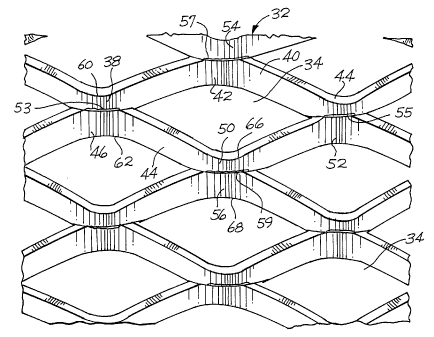
- More specifically, the expanded mesh 32 includes ~ mon(l shaped
openings 34 which are formed by perforating sheets of solid copper foil and thenexp~nding the copper foil. Each opening 34 appears to be formed by tw-o
se~nent~ or "strands" of foil. These incll~de (i) a first se~nent having an upper
left portion 36 ext~n~1in~ from a bend 38 in an u~w~u~ and rig~tw~ud direction
(when viewing FIG. 3) where it joins with an upper right portion 40 at a bend 42wherein the upper right portion 40 e~tends dow~lw~rd and righlwald to a bend 44.The second segment of foil has a lower left portion 44 e,~tentling from a bend 46 in
a dowuwa.~ and righlw~d direction where it joins with a lower right portion 48 at
a bend 50 wherein the lower right portion 48 extends u~w~d and righlwal-d to a
bend 52.
In addition, each opening 34 is formed (i) at the nine o'clock position by a
bottom edge of segment bend 38 which is connected to a top edge of segment bend
CA 0221~117 1997-09-11
46 along a connection joint 53, and (ii) at the ~ree o'clock position by a bottom
edge of segment bend 44 which is connected to a top edge of segment bend 52
along a connection joint 55. In addition, (i) at the twelve o'clock position a top
edge of segment bend 42 is connected to a bottom edge of another segment bend
54 along a connection joint 57, and (ii? at the six o'clock position a bottom edge of
segment bend 50 is connected to a top edge of another segment bend 56 along a
connection joint 59.
As shown in FIGS. 3 and 4, the individual segm~ntc of foil mesh do not lie
in the same plane. That is, during the expansion process discussed above, the foil
mesh 32 is formed into ~ifferent planes. For example, assuming there is a first
im~gin~ry horizontal plane çxtçn(lin~ ~rough connection line 53 (nine o'clock
position), a top edge or peak 60 of segment bend 38 is located the farthest distance
above t_is first im~gin~ry horizontal plane, whereas a bottom edge or peak 62 ofthe adjoining bend 46 is located the farthest distance below chis first im~gin~ry
horizontal plane. Similarly, assuming there is a second im~in~ry hori7nnt~1 plane
~rough connection line 59 (six o'clock position), a top edge or peak 66 of se~ment
bend 50 is located the farthest above ~is second im~gin~ry ho~ 1 plane,
whereas a bottom edge or peak 68 of the adjoining se~ment bend 56 is located thefarthest distance below this second im~gin~ry ho~ 1 plane. The resn1ting out
of plane configuration of the foil mesh 32 creates a mesh of peaks 66,68 extending
from opposite sides of the mesh.
The heavier weight of the mesh 32 provides additional strength to the
bowed peaks and causes them to resist compression (nolmal to t_e horizontal
planes) during fabrication of the bridge 22. In an exemplary embo~1iment the
expanded copper mesh 32 has a density of about .08 pounds per square foot and issold under the product name "AstroStrike Screening" by ~e Astroseal Company of
Old Saybrook Connecticut. After expansion, normally this expanded mesh is
- CA 0221~117 1997-09-11
rolled flat. However, for the purposes of the present invention, the fl~ttçnin~
process is deleted so that the mesh retains its out-of-plane configuration shown in
FIGS. 3 and 4.
Co~.l;....i~g with a description of the process for m~kin~ the conductive
bridge 22, the conductive mesh 32 is taped over the joint 16 as shown in FIG. 2. It
is preferable that the mesh 32 have a width dimension designated by the letter "w"
in FIG. 2 of two inches or more in order to withet~nrl the effects of a lightnin~
strike.
In the present exemplary embo~lim~nt it is desirable that the mesh have a
width ~limencion of about three inches so that it ext~n~1s laterally beyond fasteners
20. The edges of the mesh are bent dowllw~d using pliers or the like to prevent
curling so the mesh lays flat against the surface of the panel.
In order to achieve the required conductivity, the m~xi~,.. resistance
across a joint 16 which is- one meter in length is about five milliohmc. It is not
necessary that an entire joint 16 between two adjacent panels be covered by the
bridge 22, how~vel. Rather, as shown in FIG. 2, spaces 62 (between coneec~ltive
bridges 22) which are small in relation to the wavelengths of the EMI and
li~htnin~ strike energy are permi~sihle. Since these wavelengths are on the order
of about ten meters, spaces 62 of no more than about one meter between
consecutive bridges 22 are pt~rmi.eeible.
After taping the mesh 32 to the panels 14a and 14b, an epoxy adhesive is
brushed over the mesh in sufficient quantity that the entire mesh is covered with
epoxy. The a&esive must be chemically compatible with the other m~t~ri~l.e used
in the joint construction and is required to flow and envelop the conductive mesh
32 totally encasing it in resin. After cure, it is desirable that the conductive mesh
be both physically and electrically isolated from the outer (air flow) side of the
skin panel by the cured resin.
' . CA 0221~117 1997-09-11
It is preferable that the epoxy adhesive have the following properties: (1) it
must be strong enough to m~int~in a high pressure contact between the bridge
mesh 32 and the panel mesh 28; (2) it should be non-conductive so as to minimi7.e
the amount of heating within the resin when a li.~htning current flows through the
conductive mesh; and (3) it should be suf~ciently non-porous to protect the
exposed embedded wire mesh 32 from mild impact damage and corrosion. In an
exemplary embo~im~-nt, the epoxy adhesive is Type EA 956 or EA 9396
m~mlf~ctured by Hysol Corporation located in Pittsburgh, California.
Once the adhesive is applied, a Teflon~) fabric parting film (not shown) is
placed over the mesh 32. After this, a fibe'rglass bleeder fabric 69 (FIG. 5) isapplied over the parting film. The parting film pleven~ the bleeder fabric 69 from
sticking to the mesh during curing.
In order to provide a vacuum during curing, a nylon bag 70, which is
attached via a tube 72 to a vacuum pump (not shown), is attached over the covered
mesh 32 and secured to the panel by a collvt;llLional tape 74. Once this is
accompli~hed, a vacuum of a~roxi.~tely twenty eight mm Hg is drawn for about
twenty four hours to allow the adhesive to cure at room temperature.
While the adhesive is curing under vacuum, the peaks 66, 68 of the wire
mesh 32 perform several valuable functions. First, the peaks contact the exposedmesh 28 of the panel 14 to make an electrical connection thelewi~. Also, during
vacuum compression, the bridge mesh 32 is forced against the exposed panel mesh
28 c~ ing any excess adhesive there between to be squeezed out. Beneath the
peaks of the bridge mesh are open spaces 76 (FIG. 4) which provide paths for theadhesive to flow through. Without these paths for the adhesive to escape, there
would be a tendency for the adhesive to prevent the peaks of the bridge mesh 32
from contacting the panel mesh 28 during vacuum compression thereby preventing
proper electrical contact. ~~
CA 0221~117 1997-09-11
Thus, in the present process, the bridge mesh 32 remains in contact with the
panel mesh 28 during the curing process. On the other hand, if a flat or
compressible conventional mesh were used to form the bridge ~, the conventional
mesh might float away from the panel mesh 28 during the cure cycle.
In another exemplary embo~1iment the conductive bridge of the present
invention is placed across a joint between a composite panel or skin (identical to
the panel 14) and a panel made of al.. i.. l.. (not shown). In order to provide
conductivity between the composite panel and the ~l..."i",.." panel, the al~
panel is prepared by exposing a bare ~l..."i"l.... portion of this panel. Typically,
this is accomplished by removing any primer or other surface protectant from thesurface of the al.. i~.-.. ~. skin by a s~n(ling operation. Once this is accomplished, a
protective coating is applied to the bare al.. i.. l.. surface to plevt;lll oxidation and
to prepare the surface for the application of the adhesive. In an exemplary
embo(liment, this coating is a cl-ro-,late conversion coating formed by a chemical
tre~tment of the ~hlllli~ in chemical solutions coll~ -g hexavalent chr~
and goes by the name of Alodine.
After application of the protective coating, the ~l...lli,,l.,,, surface is ready
for the ~t~hment of the bridge (identical to the bridge mesh 32) in the same
m~nn~r discussed previously with regard to the ~tt~c1lment of the bridge mesh 32to the exposed panel mesh 28. Furthermore, in this exemplary embo-liment~ the
~tt~chment of the bridge mesh to the composite panel is accompli~hed in the samem~nner as discussed previously with regard to the ~t~chment of the bridge mesh
32 to the composite panel 14.