Note: Descriptions are shown in the official language in which they were submitted.
CA 02215369 1997-09-12
1
Method of Monitoring Radiation using a Floating Gate Field Effect Transistor
Dosimeter, and Dosimeter for use therein
FIELD OF THE INVENTION
This invention relates to a method of monitoring radiation using an insulated
gate
field effect transistor with a floating gate and is especially applicable to
dosimetry using
so-called "passive" MOSFET dosimeters.
BACKGROUND
Radiation dosimeters which use insulated gate field effect transistors are
well
known. Some such dosimeters comprise a "floating gate" interposed between a
control
gate and the channel between the source and the drain. When the dosimeter is
in use,
the ionizing radiation changes the charge on the floating gate which, in turn,
changes the
threshold voltage of the transistor. The change in the threshold voltage is a
measure of
the amount of ionizing radiation to which the dosimeter has been exposed.
Some floating gate dosimeters are "active", in that they require biasing in
order
for the floating gate charge to be changed by ionizing radiation. Such a
floating gate
dosimeter has been disclosed by Knoll et al in United States patent number
4,788,581
issued November 1988. The floating gate is provided between the usual control
gate and
the channel between the source and the drain. In the method of operation
disclosed by
Knoll et al, the floating gate is initially uncharged. To make the dosimeter
sensitive to
radiation, a bias voltage must be applied to the control gate. Charge
generated by
radiation in the insulating layers of the floating gate structure moves in
response to this
control gate bias, and part of the charge is collected on the floating gate.
The presence
of charge on the floating gate alters the MOSFET electrical characteristics,
which allows
the absorbed radiation dose to be determined. An experimental demonstration of
this
method of operation of a floating gate MOSFET dosimeter has been reported by
Peters
et al in an article entitled "A floating gate MOSFET gamma dosimeter", Can. J.
Phys.,
74, S685 (1996).
The need for a power supply and biasing limits the application of "active"
devices. Where the detector must be attached to or inserted into a patient
being treated
with radiation; used in space craft where power consumption must be minimized;
or
attached to a space suit worn by an astronaut during extra-vehicular activity;
or attached
CA 02215369 1997-09-12
2
to the gloved hands of persons handling radioactive materials, for example, it
is
preferable to use a "passive" dosimeter, which has its floating gate charged
before
exposure to the radiation. Irradiation causes the charge on the floating gate
to change,
causing the threshold level of the device to change also. Following
irradiation, the
"passive" device is connected to a circuit which applies bias and measures the
electrical
characteristics to determine the change in charge level and hence the amount
of radiation
to which the device was exposed.
Examples of "passive" dosimeters are disclosed in United States patent number
5,596,199 issued January 1997 naming McNulty et al as inventors, in
international patent
application number WO 95/12134 published May 1995 naming J. Kahilainen as
inventor,
and in an article entitled "Radiation Dosimeter Based on Floating Gate MOS
Transistor"
by Kassabov et al in Radiation Effects and Defects in Solids, 1991, Vol. 116,
pp. 155-
158. Insulated gate field effect transistors with floating gates are also used
in
EEPROMs, as disclosed at the Canadian Conference on Very Large Scale
Integration,
Banff, November 14-16, 1993 by G. C. McGonigal and H. C. Card in a disclosure
entitled "Analog EEPROMs with Low Programming Voltage for Adaptive Circuitry
in
Northern Telecom CMOS4S 1.2 m Technology". Although Messrs. McGonigal and
Card were concerned with providing VLSI designers with a variety of adaptive,
non-
volatile, analog and digital functions, such as neural network synaptic
weights and high-
precision circuit trimming, and did not suggest using the device for radiation
measurement, they described charging of the floating gate of an insulated gate
field effect
transistor having a floating gate, a control gate and an injector gate.
Kahilainen (WO 95/ 12134) describes a floating gate dosimeter without a
control
gate in addition to the floating gate. The floating gate is charged by
applying a
sufficiently high voltage between the source and drain to cause tunnelling to
occur
through the oxide layer of the gate insulator. The other devices each have a
floating gate
interposed between a control gate and the channel. Thus, Kassabov et al charge
the
floating gate by applying voltage impulses to the control gate. Likewise,
McGonigal and
Card charge the floating gate by applying "programming pulses" to the control
gate.
McNulty et al charge the floating gate by applying a negative voltage between
the source
and the drain such that electrons from the drain are "swept up" to the
floating gate by
the more positively charged control gate, which is held at a constant voltage.
A disadvantage of these known methods of charging the floating gate is that
they
CA 02215369 2007-08-01
3
may result in interface states which can give noise and long-term stability
problems,
particularly in view of the relatively high sensitivity involved in most
radiation
measurements.
A fiuther disadvantage of known passive dosimeters is their susceptibility to
tempexatuxe variations. The threshold voltage VT of a MOSFET varies in
dependence
upon temperature, which is of concern for a MOSFET dosimeter, since a change
in VT
in response to temperature variation could be falsely interpreted as an
indic$tion of
exposure to radiation. It is known to operate a pair of active MOSFET
dosimeters
differentially to compensate for temperature variations. Thus, United States
patent
XQ number 4,678,916 issued July 1987, naming I. Thomson as imwemtor, discloses
a
dosimeter comprising a pair of insulated gate geld effect transistors
integrated into the
same substrate but biased to dxfferent levels during radiation measurement.
The output
of the dosimeter is the difference between the threshold voltages of the two
MOSFETs.
Both threshold voltages will be affected to substantially the same degree by
temperature
variations, but the difference will be substantially unaffected. Although this
approach
has been used with active dosizneters, the methods of charging the floating
gates of the
above-mentioned known passive dosimeters are too irxtpzecise for satisfactory
differential operation.
An object of the present invention is to eliminate or at least ameliorate the
disadvantages of the known method of monitoring radiation using passive
floating gate
dosimeters and to provide an improved method ofmonitoring xad.iation and a
dosimeter
for use therein.
SUMMARY OF THE INVENTION
According to a first aspect oft,he present invention, there is provided a
method
of monitoring ionizing radiation using an insulated gate field effect
transistor having a
source and a drain formed in a substrate, a floating gate separated from the
substrate by
an insulating layer, a control gate overlapping a first part of the floating
gate and
insulated therefrom, and a charging gate overlapping a second part of the
floating gate
and insulated therefrom, the second part being reznote from a chaun,el between
the
source and drain. The method comprises the steps of:
(i) main,tainingpotential differences between the substrate, source, drain and
control
gate lower than a maximum normal operating voltage of the transistor;
CA 02215369 2007-08-01
4
(ii) establishing a potential difference between the charging gate and the
control gate,
monitoring a parameter dependent upon a threshold voltage of the transistor,
and
increasing the potential difference to cause a transfer of charge between the
charging
gate and the floating gate throughthe insulating layer material between the
charging gate
and the floating gate until a predetercxzined threshold voltage is established
without
involving excessive electric field stress in the region of the chmuel;
(iii) with the substrate, source, drain, control gate and charging gate
connected in
common, exposing the transistor to the ionizing radiation; and
(iv) following such irz=adiation, determining the amount of such ionizing
radiation
absorbed by the dosimeter by measuring a parameter affected by change in the
charge
applied to the floating gate.
This method of charging avoids a relatively high electric field strength in
the gate
oxide between the floating gate and the channel, and avoids a r latively high
electric
stress at the surface of the channel. Preferably, such electric field stress
is kept below
a level which would cause the creation of states capable of trapping charge at
the
channel surface.
Preferably, the parameter measured to deterrnine the amount of radiation is
the
same parameter that was monitored during charging of the device. Thus, the
absorbed
radiation dose may be measured by applying a fixed drain-source bias,
measuring the
drain current, and adjusting the control gate bias until the drain current is
the same as
that measured during pre-charging of the floating gate_ 'T,'be control gate
bias to achieve
this drain current is equivalent to the threshold voltage of the device.
According to a second aspect of the invention, there is provided a method of
monitoring ionizing radiation using a dosimeter comprising a matched pair of
insulated
gate field effect transistors sharing a common substrate, each having a source
and a
drain formed in the substrate, a floating gate separated from the substrate by
an
insulating layer, a control gate overlapping a first part of the floating gate
and insulated
therefrom, and a charging gate overlapping a second part of the floating gate
and
insulated froxn both the floating gate and the control gate, the second part
being remote
from a channel between the source and drain, the method comprising the steps
of:
(i) maintaining potential differences between the substrate, source, drain and
control
gate of each transistor lower than a maxamuxn normal operating voltage of the
transistors;
(ii) establishing a potential difference between the char&g gate of one of the
CA 02215369 1997-09-12
transistors and its control gate, monitoring a parameter dependent upon a
threshold
voltage of the one transistor and increasing the potential difference to
transfer charge
between the charging gate and the floating gate, through the insulating
material layer
between the charging gate and the floating gate, until a predetermined
threshold voltage
5 is established without involving excessive electric field stress in the
region of the channel
of that transistor;
(iii) establishing a potential difference between the charging gate of the
other of the
transistors and its control gate, monitoring a parameter dependent upon a
threshold
voltage of said other of the transistors and increasing the potential
difference to transfer
charge between the charging gate and the floating gate, through the insulating
material
layer between the charging gate and the floating gate, until a predetermined
threshold
voltage is established without excessive electric field stress in the region
of the channel
of such other transistor;
(iv) with the substrate, sources, drains, control gates and charging gates
connected in
common, exposing the dosimeter to the ionizing radiation; and
(v) following such irradiation, determining the amount of such ionizing
radiation
absorbed by the device by measuring a parameter dependent upon the difference
between
the threshold voltages of the pair of transistors.
Preferably, the floating gates of the two transistors are charged to equal and
opposite levels.
According to a third aspect of the invention, there is provided a dosimeter
comprising a matched pair of insulated gate field effect transistors sharing a
common
substrate, each of said transistors having a source and a drain formed in the
substrate,
a floating gate separated from the substrate by an insulating layer, a control
gate
overlapping a first part of the floating gate and insulated therefrom, and a
charging gate
overlapping a second part of the floating gate and insulated from both the
floating gate
and the control gate, the second part being remote from a channel between the
source
and the drain.
Further objects and features of this invention will become clear from the
following description of preferred embodiments, which are described by way of
example
only and with reference to the accompanying drawings.
CA 02215369 1997-09-12
6
BRIEF DESCRIPTION OF THE DRAWINGS
Figure 1 is a schematic plan view of a portion of a dosimeter comprising a
MOSFET;
Figure 2 is a cross-sectional partial view of the MOSFET taken on the line II-
II
of Figure 1;
Figure 3 is a cross-sectional partial view of the MOSFET taken on the line III-
III
of Figure 1;
Figure 4A is a simplified schematic diagram of a circuit for measuring the
threshold voltage of the MOSFET of Figure 1;
Figure 4B is a simplified schematic diagram of a circuit for charging the
MOSFET of Figure 1;
Figure 5 is a schematic plan view of a differential dosimeter comprising a
pair
of MOSFETs sharing a common source and arranged for differential biasing;
Figure 6 illustrates the change in threshold voltage of one of the MOSFETs of
Figure 5 when the other is left uncharged as a reference;
Figure 7 illustrates the sensitivity of the dosimeter of Figure 5 as a
function of
absorbed dose when only the one MOSFET has been charged;
Figure 8 is a simplified schematic diagram of a circuit for measuring the
radiation
absorbed by the differential dosimeter of Figure 5; and
Figure 9 illustrates the change in threshold voltage for the two MOSFETs of
Figure 5 as a function of absorbed dose when they have been charged
oppositely.
DESCRIPTION OF PREFERRED EMBODIMENTS
In the drawings, corresponding or identical elements in the different Figures
have
the same reference numeral.
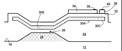
For purposes of illustration, Figures 1, 2 and 3 illustrate the structure of a
p-
channel floating gate MOSFET dosimeter 10. It should be appreciated, however,
that
the invention is applicable, mutatis mutandis, to n-channel devices. The
MOSFET
dosimeter comprises a substrate 12 (Figure 2) with a source 14 and drain 16
formed in
its surface 18. The source 14 and drain 16 have terminals 20 and 22,
respectively. An
insulating layer 24 provided on the surface 18 of substrate 12 comprises a
relatively thin
region of gate oxide 26 over the channel 28 between the source 14 and drain
16, and
thicker field oxide portions around the channel. A floating gate 30, formed
from a layer
CA 02215369 2002-08-19
7
of conductive material, comprises a rectangular portion 30A, an elongate
portion 30B which
extends from the middle of one edge of the rectangular po--tion 30A, and a
small rectangular
protrusion 30C which protrudes from the opposite edge of the rectangular
portion 30A. The
elongate portion 30B extends between the source 14 and drain 16 and is
isolated electrically
from the channel 28 by the gate oxide 26. A second insulating layer 32 covers
the floating
gate 30. A control gate 34, also of conducting material and having a terminal
36, is provided
upon the second insulating layer 32 and overlies the floating gate 30. In
Figure 1, the control
gate 34 is shown slightly smaller than the floating gate rectangular portion
30A, but it could
be the sanle size or even slightly larger. A charging gate 38, which is much
smaller than
control gate 34, overlies the protrusion 30C of the floating gate 30 and is
insulated from it
by the insulating layer 32. The charging gate 38 has a terminal 40.
Preferably, the floating gate 30, control gate 34 and charging gate 38 are
formed from
polysilicon and the insulating layers 24 and 32 fi-om thermally-grown silicon
dioxide.
To prepare the dosimeter for use, charge is placed upon the floating gate 30,
causing
a shift in the threshold voltage V.,,. (The threshold voltage V,- of the
MOSFET is defined in
this specification to be the control gate bias required to give an arbitrarily-
specified channel
current at a given drain-source bias VD,;). There is no electrical connection
to the floating
gate 30 which, as can be seen from the cross-sectional views of Figures 2 and
3, is electrically
isolated from the channel region 28 by the gate oxide 26 and from the control
gate 34 by the
insulating layer 32. The charging gate 38 is used to charge the floating gate
30 prior to use
of the dosimeter for radiation monitoring. Because the charging gate 38 is
remote from the
channe128, the charging can be done without stressing the gate oxide region 26
and channel
28. Charge is applied to the floating gate 30 by maintaining the substrate 12,
source 14, drain
16, and control gate 34 at voltages such that the potential difference between
any two of
them is less than the maximum normal operating voltage of.'the MOSFET,
typically 5 volts,
while a voltage bias greater than the maximum normal operating voltage is
applied to the
charging gate 3 8.
Before the floating gate 30 is charged, however, the threshold voltage of the
MOSFET 10 is measured since the absorbed radiation dose will be determined by
comparing
threshold voltage levels before and after irr-adiation.
CA 02215369 1997-09-12
8
Figure 4A shows a simple measuring circuit for measuring the threshold voltage
of the MOSFET 10. The source 20, substrate 12, and charging gate 38 are
connected to
a supply rail at a fixed potential +VDD, typically 1 volt. The drain 22 is
connected by
resistor R to a negative supply rail at voltage -VDD, and the control gate 34
is connected
to the output of the operational amplifier 42. A digital voltmeter is
connected to the
output of the operational amplifier 42 to measure the threshold voltage. In
operation,
the conductance of the MOSFET channel is adjusted automatically to the
conductance
of the resistance R (typically around 100 Kilohms to give a drain current of
about 10
microamp. The output of the operational amplifier 42 then is the threshold
voltage, as
defined herein. Once the initial threshold voltage has been measured, the
floating gate
30 is charged by means of the circuit shown in Figure 4B, which differs only
slightly
from that of Figure 4A.
Referring now to Figure 4B, the circuit for placing (negative) charge upon the
floating gate 30, thereby making the threshold voltage more positive,
comprises a
feedback loop including an operational amplifier 42. The inverting input of
the amplifier
42 is grounded. The non-inverting input is connected to the drain terminal 22,
and, via
a resistor R, typically of 100 Kilohms, to a supply rail at +VDD volts. The
output of the
amplifier 42 is connected to the charging gate 38. The source terminal 20 and
substrate
12 are connected to a supply rail at voltage +VDD while the terminal 36 of
control gate
34 is connected to a source of a bias voltage VGG.
Applying a positive bias to the charging gate 38 places a positive charge on
the
floating gate 30, while applying a negative bias leaves a negative charge on
the floating
gate 30. Assuming that the initial measurement shows that the threshold
voltage of the
device is more negative than the desired threshold voltage, the control gate
bias Vm is
set to the desired threshold voltage. Assuming the magnitude of the drain
current ID
initially is less than the target value VDD/R, the operational amplifier 42
makes the
charging gate bias more negative until electrons tunnel between the charging
gate 38 and
the floating gate 30. The extra negative charge on the floating gate 30
attracts holes to
the channel surface, increasing the drain current ID. The feedback loop forces
this
process to continue until drain current ID reaches the target value.
If the initial measurement shows that the threshold voltage is more positive
than
the desired target threshold voltage, the circuit of Figure 4B can also used
to apply
positive charge to the floating gate 30, thereby forcing the threshold voltage
more
CA 02215369 1997-09-12
9
negative. Once again, the control gate bias is set to the desired threshold
voltage. The
magnitude of the drain current 'D is initially greater than the target value
VDD/R, so the
operational amplifier 42 makes the charging gate bias more positive until
electrons tunnel
from the floating gate 30 to the charging gate 38, giving the floating gate 30
a net
increase in positive charge. The extra positive charge on the floating gate 30
repels
holes from the channel surface, reducing drain current ID. The feedback loop
forces this
process to continue until drain current 'D reaches the target value.
The bias voltage applied to the control gate is small, typically no greater
than the
maximum normal operation voltage, and there is no potential difference between
any two
of the substrate, source, drain and control gate which is greater than the
maximum
normal specified operating voltage of the device.
The bias voltage applied to the charging gate 38 is much greater, being
sufficient
for Fowler-Nordheim tunnelling to cause electrons to flow between the charging
gate 38
and the floating gate 30 through the interpoly oxide 32 separating them.
Tunnelling
occurs first through the portion of insulator 30 separating the charging gate
38 and the
floating gate 30 since, because the area of overlap of the charging gate 38
with the
floating gate 30 is much smaller than the overlap of the control gate 34 with
the floating
gate 30, the capacitance between the charging gate 38 and the floating gate 30
is much
smaller than that between the floating gate 30 and control gate 34.
Accordingly, most
of the potential difference applied between the charging gate 38 and the
control gate 34
is dropped between the floating gate 30 and the charging gate 38.
This method of pre-charging is preferred because it does not require high
electric
field strengths in the vicinity of the sensitive channel area of the MOSFET,
i.e. the gate
oxide 26 and channel 28. Electric stress in the channel area is believed to
generate fast
surface states or "interface traps", perhaps leading to noise and long-term
stability
problems.
To use the pre-charged MOSFET dosimeter for radiation detection, the source
14, drain 16, substrate 12 (body), control gate 34 and charging gate 38 are
connected
together electrically. It should be noted that no connection to a battery or
other external
power supply is required during radiation detection. If any ionizing radiation
capable
of generating electron-hole pairs in the gate oxide, field oxide and/or inter-
gate insulators
passes through the device, the floating gate 30 will be partially discharged.
This in turn
produces a shift in the threshold voltage, from which the absorbed dose can be
deduced.
CA 02215369 1997-09-12
In general, the relationship between the change in threshold voltage and the
absorbed
dose must be determined empirically for a given device geometry and
manufacturing
process. Once the relationship is established, it can be applied to any device
of the same
dimensions manufactured with the same process.
5 The sensitivity of a MOSFET dosimeter is defined in the art as the ratio of
the
shift in threshold voltage to the absorbed radiation dose. This sensitivity
can be adjusted
by varying the relative sizes of the control gate 34 and floating gate 30. The
smaller the
area of the control gate 34 relative to the floating gate 30, the larger will
be the shift in
threshold voltage (as defined above) in response to a given dose of ionizing
radiation.
10 Hence, making the area of control gate 34 much smaller than that of the
floating gate
portion 30A would provide increased sensitivity. It should be noted, however,
that
making the area of the control gate 34 small relative to the floating gate 30
also increases
the magnitude of random fluctuations in the measured threshold voltage
resulting from
random changes in interface trap occupancy. In consequence, gains in
sensitivity
obtained by this technique may be offset by an increase in noise. In a given
application,
the relative area of overlap of the control gate over the floating gate
compared to the
overlap of the floating gate over the channel and field regions should
preferably be made
small enough that the noise generated by the MOSFET sensor is larger than that
produced by other components in the circuitry used to determine the threshold
voltage.
There is no advantage to further reduction in the area of control gate
overlapping the
floating gate.
Typically, the threshold voltage of a MOSFET dosimeter will change by
approximately 2 mV for a 1 C change in temperature. In order to reduce the
effects of
such variations, a matched pair of MOSFET dosimeters may be fabricated on a
common
substrate, as shown in Figure 5, in which corresponding elements have the same
reference numbers as in Figures 1-3, but with a suffix 1 or suffix 2, and the
various
materials are the same as those used in the embodiment of Figure 1.
Referring to Figure 5, a common source 14' is provided between a pair of
drains
16/1 and 16/2, which define respective channels (not shown) between the drains
and the
common source 14. A first floating gate 30/1 has a rectangular extension
portion 30A/1
and an elongate portion 30B/1 extending across the channel 28/1. In contrast
to the
MOSFET of Figure 1, where the elongate portion protrudes from the middle of
the
rectangular portion, this elongate portion 30B/1 protrudes from the corner of
the
CA 02215369 1997-09-12
11
rectangular portion adjacent the channel 28/1. A first control gate 34/1 is
provided
above the floating gate 30/1 and separated therefrom by insulating material
(not shown).
A control gate terminal 36/1 with a terminal extension 37/1 is attached to one
corner of
the edge of the control gate remote from the drain 16/1. The other corner of
the same
edge of the control gate 34/1 is notched to leave a rectangular area 40/1 of
the floating
gate 30/1 uncovered. A small rectangular charging gate 38/1 is provided in the
notched
area 40/1 and carries a charging gate terminal 44/1.
The second MOSFET comprises a second floating gate 30/2, second control gate
34/2, second control gate terminal 36/2, second charging gate 38/2 and second
charging
gate terminal 44/1 disposed at the opposite side of an axis 46 through the
common source
14' and perpendicular to an axis 48 joining the two drains 16/1 and 16/2. The
gates of
the second MOSFET are configured as a mirror image to the corresponding gates
of the
first MOSFET about the axis 46 through the common source 14'.
Because these two MOSFETs are formed in close proximity on the same silicon
integrated circuit, they must be at almost exactly the same temperature, since
the power
dissipation in the transistors is extremely small for operation as a
dosimeter. The two
MOSFETs are identical in structure. Different charges are placed on the
floating gates
30/1 and 30/2 of the two MOSFETs by means of the charging gates 38/1 and 38/2,
respectively. This leaves the two MOSFETs with different threshold voltages.
The
output of the dosimeter is taken to be the difference OVT between the
threshold voltages
VT/1 and VT/2 of the two devices. Since the floating gates have different
initial charges,
the change in VT under irradiation is different for the two MOSFETs, so there
is a net
change in OV,..
A floating gate MOSFET dosimeter as shown in Figure 5 has been constructed
and tested. Fabrication of the dosimeter was carried out using the Mitell.5 CM-
channel
technology by Mitel Semiconductor Ltd. of Kanata, Ontario, Canada. The gate
material
was polysilicon, and the insulating layers were of thermally grown silicon
dioxide. The
gate oxide thickness was 27 nm, the field oxide thickness 600 nm, and the
interpoly
oxide thickness 48 nm. The length and width of each channel were both 20 m
while
the floating gate and control gate extensions over the field oxide were
approximately 200
m by 50 m. The charging gate was 6 m by 6 m.
Prior to irradiation, the floating gates of both MOSFETs were discharged by
exposure to ultra violet light from a commercial EPROM eraser for a period of
many
CA 02215369 1997-09-12
12
hours. Using a circuit like that shown in Figure 4A, the threshold voltages of
both
devices were determined by setting VSB = 0, VDS = 0.1 V, and finding the value
of Vcs
required to give ID = 10 A. Following this procedure, threshold collapse VT
was found
to be -2.5 V for both devices. A negative bias was then applied to the
charging gate
of one MOSFET, while all other source, drain, control gate and substrate
terminals of
the two MOSFETs were maintained at a common potential (ground). The charging
gate
bias was then increased until the current through the charging terminal
reached a value
of approximately 10 picoamps. The current was held at this level for several
seconds.
At the completion of this operation, the threshold voltage of the charged
MOSFET had
increased to 7 V. The charge on the floating gate of the other MOSFET was
unchanged.
Following charging, the dosimeter was covered with a 5 mm thick acrylic sheet
and exposed to a 6 kCi 60Co source at a distance of 1 meter. The change in
threshold
voltage for the two MOSFETs as a function of absorbed dose is shown in Figure
6.
Under irradiation, the threshold voltage for the pre-charged MOSFET decayed
towards
that of the other device, which remained substantially constant. The dosimeter
output -
the difference OVT between their threshold voltages - is shown as a function
of absorbed
dose in Figure 7.
As can be seen from Figure 7, which illustrates the sensitivity of the
differential
dosimeter of Figure 5 as a function of absorbed dose when only one MOSFET is
charged, the sensitivity decreases as the amount of absorbed radiation
increases.
Subsequently, the following charging procedure was found to be preferable:
With the substrate and source terminals grounded, a voltage equal to the
desired
threshold voltage, typically 5 volts was applied to the control gate and a
voltage of -
1 volt applied to the drain terminal:
1. The drain current 'D was monitored.
2. The bias voltage at the charging gate was set to positive or negative
depending
upon whether the drain current 'D was above or below the required level of,
say, 10 A.
(If, say, 'D was zero, the voltage applied to the charging gate would be
negative).
3. The voltage on the charging gate 38 was increased in magnitude gradually
until
the drain current reached 10 A. Typically, this voltage would be swept from,
say, 20
volts to 30 volts, i.e. much greater than the normal operating voltage of 5
volts.
For optimum sensitivity, equal and opposite charges are applied to the
floating
gates 30A/1 and 30A/2 by means of their respective charging gates 38A/1 and
38A/2
CA 02215369 1997-09-12
13
using the circuit of Figure 4B. Following irradiation, the radiation dose or
absorbed
radiation is determined by applying identical fixed drain-source and source -
substrate
biases, and varying the gate-source bias of each device until the drain
current in each is
identical.
A suitable circuit for measuring the change in the difference between the
threshold voltage levels, as shown in Figure 8, effectively duplicates the
measuring
circuit of Figure 4A. Hence, it comprises two operational amplifiers 42/1 and
42/2,
respectively, each connected in a feedback loop with a corresponding one of
the pair of
MOSFETs 10/1 and 10/2. Each amplifier has its non-inverting input connected to
the
drain of its transistor which also is connected to the negative supply rail at
voltage -VDD
via a resistance of, typically, 100 kilohms. The substrate, source and
charging gate are
connected to a positive supply rail at voltage +VDD. The inverting input of
the amplifier
is grounded and its output is connected to both the control gate and to a
respective one
of two differential inputs of digital voltmeter 56. Typically, VDD is about 1
volt. With
the control gates set to the respective threshold voltages (previously
measured), the
voltage measured by the digital voltmeter is the difference between the
threshold voltages
and hence a measure of the differential change in the charge on the two
floating gates.
Figure 9 illustrates how the threshold voltages of the two devices change as a
function of absorbed dose. It should be noted that operation with opposite
polarity
charging of the two floating gates enhances sensitivity as compared with the
known
passive dosimeters. In fact it would be approximately double that depicted in
Figure 7
for the matched pair with only one of the MOSFETS charged.
Although, in the specific embodiments described herein, the voltage bias
applied
to the charging gate was greater than the maximum normal operating voltage, it
is
envisaged that, in certain circumstances, a lower voltage could be used.
The measurement of the threshold voltage changes may be done manually or by
means of electronic data logging equipment.
In the above-described embodiments, the relatively large floating gate
extension
portion 30A also provides increased sensitivity to radiation. Because the
field oxide is
much thicker than the gate oxide in conventional CMOS technology, far more
charge is
generated by radiation in the field oxide than in the gate oxide. It is
therefore highly
advantageous to overlap the floating gate over the field oxide, to facilitate
collection of
radiation-generated charge from this oxide.
CA 02215369 1997-09-12
14
If yet greater sensitivity were required, the rectangular extension 30A could
be
duplicated on the other side of the channel 28. Various other modifications
may be made
to the above-described embodiments within the spirit and scope of the present
invention.
An advantage of dosimeters embodying the present invention is that they may be
fabricated using conventional, commercial CMOS processes. Moreover, the
dosimeters
can be discharged and re-charged many times with full recovery of the initial
sensitivity,
unlike known devices which do not fully recover, or must be annealed at
relatively high
temperatures.