Note: Descriptions are shown in the official language in which they were submitted.
CA 02215376 1997-09-15
WO 96/28890 1 PCT/LTS96102559
DIRECT DIGITAL SYNTHESIZER DRIVEN PLL FREQUENCY SYNTHESIZER WITH CLEAN-UP PLL
BACKGROUND OF THE INVENTION
I. Field of the Invention
The present invention relates to frequency synthesizers. More
particularly, the present invention relates to a novel and improved
apparatus and method for frequency synthesis utilizing a direct digital
synthesizer in combination with one or more phase lock loops.
II. Description of the Related Art
Conventional frequency synthesis may be accomplished using a direct
digital synthesizer in combination with a phase lock loop. Direct digital
synthesizers (DDS) can be used to provide a loop reference signal for the
phase lock loop. Ideally, a phase lock loop (PLL) is designed to reject spurs
from the DDS reference signal, operate over a wide frequency range and
achieve a rapid settling time. Achieving all these design goals, however,
may be difficult utilizing a single PLL iri combination with a DDS. A PLL
designed to settle quickly on a new frequency is often unable to reject a wide
range of spurs found on the DDS reference signal. Decreasing the frequency
settling time and increasing spur rejection present conflicting design
requirements in a PLL device.
The DDS reference signal is a digitized periodic signal whose
frequency can be finely tuned over a given bandwidth. This signal is
produced by accumulating phase at a higher rate consistent with sampling
theory, translating the phase into a periodic waveform via a lookup table,
and converting the resulting digital representation of the periodic
waveform to an analog signal using a digital to analog converter. The DDS
output signal, however, may contain spurs due to quantization errors and
truncation as well as noise due to thermal and semiconductor effects.
The analog signal, produced by the DDS, is the reference frequency
source for the PLL. A PLL is designed to output a range of frequencies where
the frequency resolution is equal to the reference frequency. Coarse output
frequency adjustments in increments of the nominal DDS reference
frequency, may be made by varying the loop divisor value. The fine
CA 02215376 2005-08-04
74769-95
2
frequency adjustments may be made by varying the DDS output frequency,
e.g. the source of the phase lock loop reference frequency. The fine
adjustment increment is the frequency resolution of the DDS output
multiplied by the value of the loop division.
The performance of a phase lock loop is related to several factors
including (1) the frequency of the reference signal, (2) the magnitude of the
divisor necessary to divide the output frequency down to the reference
frequency, and (3) the bandwidth of the loop filter. The frequency of the
reference signal dictates the frequency resolution, or step size of the loop,
i.e.
the smaller the reference frequency, the greater the frequency resolution.
The magnitude of the loop divisor has great impact on the noise
performance of the loop. As such, any phase noise or spurious noise in the
reference frequency will appear in the loop output having its original
magnitude multiplied by the loop divisor. The bandwidth of the loop filter,
which is normally five to ten percent of the reference frequency or less,
impacts the speed with which the loop can settle on a new frequency. Thus
the narrower the loop filter bandwidth, the slower the loop will be able to
settle on the new frequency.
The conventional DDS driven PLL synthesizer can synthesize signals
with fine frequency resolution and high spectral purity. A PLL designed
with a narrow bandwidth loop rejects noise and spurs from the DDS
reference signal and produces a signal with high spectral purity. Examples
of DDS driven PLL synthesizers are provided in U.S. Patent No. 4,965,533
entitled "DIRECT DIGITAL SYNTHESIS DRIVEN PHASE LOCK LOOP
FREQUENCY SYNTHESIZER" and U.S. Patent No. 5,028,887 entitled
"DIRECT DIGITAL SYNTHESIZER DRIVEN PHASE LOCK LOOP
FREQUENCY SYNTHESIZER WITH HARD LIMITER" which are by the
present inventor assigned to assignee of the present invention.
The small band~n~idth loop required to
obtain high spectral purity, however, tends to increase frequency settling
time. In a conventional DDS driven PLL synthesizer, fast settling time and
high spectral purity present conflicting design requirements.
It is therefore an object of the present invention to provide a novel
and improved direct digital synthesizer driven phase-lock loop frequency
5J synthesizer capable of achieving a fast settling time while producing a
signal
with high spectral purity.
It is another object of the present invention to provide a novel and
improved direct digital synthesizer driven phase lock loop frequency
CA 02215376 1997-09-15
WO 96128890 3 PCT/US96/02559
synthesizer where the direct digital synthesizer does not require the use of a
digital-analog-converter.
A further object of the present invention is to utilize a switching
arrangement to reduce the settling time of an improved direct digital
synthesizer driven phase lock loop frequency synthesizer.
SUMMARY OF THE INVENTION
An improved frequency synthesizer uses a pair of phase lock loop
circuits to process a digitally generated analog signal. A direct digital
synthesizer (DDS) is one method of producing the digital reference signal.
The DDS produces digitized periodic frequencies by accumulating phase at a
higher rate consistent with sampling theory, translating the phase into a
periodic waveform via a lookup table, and converting the resulting digital
representation of the periodic wave to an analog signal using a digital to
analog converter.
In the first embodiment, the first or clean-up PLL coupled to the DDS
frequency source cleans up close-in noise around the reference frequency.
The clean-up PLL offers advantages over conventional filter arrangements
because it will inherently track the provided reference frequency. Filtering
capabilities of a PLL depend on the size of the loop bandwidth. A narrower
PLL loop bandwidth will filter out frequencies in a smaller window around
the reference frequency. Typically, the clean-up PLL produces an output
signal close to, or the same as, the input reference frequency by setting the
loop divisor value to substantially unity. A clean-up PLL will provide a
spectrally pure reference signal independent of any additional filters that
may be required by other conventional synthesizers.
A second or primary PLL circuit accepts the spectrally pure reference
signal from the clean-up PLL and adjusts the frequency as needed. The PLL
circuit adjusts the output frequency, in increments of the input reference
frequency, by adjusting the loop divisor value to values substantially greater
than unity. A frequency control input to the primary PLL can be used to
dynamically make coarse adjustments to the output frequency. Fine
frequency control can be achieved by adjusting the DDS reference frequency
used as input to the first of the PLL circuits.
The overall settling time for the present embodiment to lock onto a
new signal depends on the loop bandwidth of each PLL and the individual
probability each PLL will lose lock with the provided signal. The clean-up
CA 02215376 1997-09-15
WO 96/28890 4 PCT/US96/02559
PLL produces an output frequency closely matching the input reference
frequency and during operation will typically not lose lock. As a result, the
longer settling time associated with the clean-up PLL's narrow loop
bandwidth does not contribute significantly to the overall settling time
equation. The primary PLL, which typically does break signal lock when
making large frequency adjustments, reduces settling time by having an
arbitrarily large loop bandwidth.
The settling time of the present embodiment is greatly improved by
utilizing two PLL circuits. Conventional DDS driven PLL synthesizer
designs, typically using only one PLL, are constrained by mutually exclusive
close-in filtering and fast frequency settling time design requirements. In
present embodiment a clean-up PLL separates the close-in filtering function
from the fast frequency settling time requirement and thus adds an
additional degree of freedom to the settling equation for a frequency
synthesizer. The primary PLL in the present embodiment is no longer
required to perform close-in filtering and instead can be designed to have an
arbitrarily fast frequency settling time.
The present embodiment may also be used to simplify design
requirements for digital reference frequency synthesizers. A typical digital
frequency synthesizer comprises a direct digital synthesizer (DDS) coupled
to a digital to analog converter (DAC) element. The present embodiment
will also work with a frequency synthesizer not utilizing a DAC. Instead of
utilizing the DAC output, the most significant bit (MSB) from the DDS
accumulator is provided directly to the clean-up PLL. The filtering qualities
of the clean-up PLL eliminate harmonic spurs present on the DDS MSB
signal and produces a sine-wave signal. The resulting sine-wave signal can
readily be used by the primary PLL for further signal processing.
An alternative embodiment utilizes a switching apparatus to
minimize any settling time which may be contributed by the clean-up PLL
in the present invention. This embodiment uses a power splitter means for
creating a first and second duplicate of the digitally generated periodic
signal.
The first duplicate periodic signal is provided to the clean-up PLL and a
subsequent switching means for selectively passing the signal through a
power summer means and to the primary PLL circuit. This switching
means is responsive to a control signal produced by a switching control
circuit.
The second duplicate periodic signal is provided directly to a
switching means capable of selectively passing the signal through a summer
CA 02215376 2003-03-10
74769-95
means and to the primary PLL circ:ui.t. This switching means
is also responsive to a control signal produced by a
switching control -~.ircuit..
This swif~cr,~,inc3 embodiment bypasses the clean-up
5 PLL while it settles on the rzew frequency. This reduces the
overall settling tr.me by eli_minatir~g settling time delay
which may be r_ontri.bute~~ by t;he clean-up PLL. When a
frequency change occurs the switching control produces
control si.gnal.s whi.c:h opens i_:he switch associated with the
clean-up F'LL and closes the :,witch associated with the
second duplicate pEricdic signal. Dncve the clean-up PLL has
settled onto the new frequency, the switch associated with
the clean-up FLL closes and t:he switch associated with the
second duplicate periodic signal then. opens.
The preferred embodiment=s c~f the present invention
provide several advantages over the prior art. The settling
time can be improve~~ b;r usincv one PIJIJ as a "c:lean-up"' filter
for the DDS reference signal and a second 2LL as frequency
multiplier. A clean-v.zp PLL remove>s DDS spurs while
continuously tracking -the phase continuous DDS output..
Maintaining frequene:y and phase lock :between the clean-up
PLL and the DDS output. minimizes the settl.i.ng time of this
loop. Meanwhile, a .:~r::c~ond I?LL c7perates as a frequency
multiplier. Increasing the loop bandwidth in the second PLL
allows a wide i=requErzcy :bandwidth output along with a fast
frequency switching character~.st:ic.
Accoz:ding to one br~_aad aspect of the invention
there is provided a frequency synthesizer ~~omprising: a
frequency source for:' digital.l'~ generating a variable
frequency signal; a first phase lock loop circuit having a
first predetermined loop band4vidth coupled to said frequency
CA 02215376 2003-03-10
74769-95
Sa
source; a second please lock loop circuit having a second
predetermined loop bandwidth greater than said first
predetermined loop bandwidth coupled to said first phase
lock loop cirr_,uit; a power sputter disposed between said
frequency soumce arid said first phase lock loop circuit,
said power splitter having ar.~ input arzd first and second
outputs, said power sf>l:itter input coupled to an output of
said frequency soux:ce and said power sputter first output
coupled tc said first phase =.ock loop circuit; a first
switch, responsive to a first: SWitCh control signal,
disposed between said First phase lock loop circuit and said
second phase lack loop circuit; a. summer disposed between
said first swil~ch and said se:.-:ond phase lock loop circuit,
said summ.e.r having first and ~~econd inputs and an output,
said summer first input. coupled to ;paid first switch and
said summer output a::oupled to said second phase lock loop
circuit; and a second switch, resporaive to a second switch
control signal, cou~:>led to said power splitter second output
and said summer. secc>nd input .
P.ccording to one brc-_~ad aspect of the invention
there is provided a method of frequency synthesis comprising
the steps of: digit.a.l.ly generating a variable frequency
reference signal; spi.itting said variable frequency
reference signal into a first. branch reference signal and a
second branch reference signal.; filtering said first branch
reference signal in a first prease lock loop circuit having a
first predetermined :1<aop bandwidth; applyin<3 said filtered
first branch reference signal to a reference. input of a
second phase lock loop circuit having a second predetermined
loop bandwidth :i.n re;:~;pomse to a first. switch control signal;
and applying said second branctn reference signal to said
reference input of said second phase lock loop circuit in
response to a second sw;.tch co°~trol signal.
CA 02215376 2003-03-10
74769-95
5b
BRIEF DESCRIPTION OF THE DRAWINGS
The features, objec-_~ts, and advantages of the
present invention will become more apparent from the
detailed description set forth below when taken in
conjunction with the drawings in whicrl like reference
characters identify correspondingly throughout and wherein:
Figure 1 il.lustrate~s a prior art direct digital
synthesizer (DDS) driven. phase lcck loop iPLL) frequency
synthesizer;
Figure 2 i_ll.mstrates one embodiment of the present
invention for a DDS driven (PILL) frequency synthesizer with
a clean-up PLL;
Figure 3 illustrate;~~ a first alternative
embodiment of the Dr;S driven l?LL of the present invention;
and
Figure 4 i.llustrate;~ a. second alr_ernative
embodiment of t:he DDS driven PLL o:f she present invention.
CA 02215376 1997-09-15
WO 96/28890 6 PCT/L1S96/02559
DETAILED DESCRIPTION OF THE PREFERRED
EMBODIMENTS
The preferred embodiment of the present invention provides many
advantages over prior art frequency synthesizers. FIG. 1 illustrates in block
diagram a conventional direct digital synthesizer (DDS) driven phase lock
loop (PLL) frequency synthesizer 100. Synthesizer 100 typically comprises a ~ -
frequency synthesizer 101 and a phaselock loop circuit (PLL) 114 used in
combination to provide a desired synthesized output frequency 124.
. Frequency synthesizer 101 is typically comprised of DDS 102, digital to
analog converter (DAC) 108, filter 110 and optionally a frequency divider
112. In the embodiment illustrated in FIG. 1, DDS 102 is comprised of phase
accumulator 104 and sine lookup table 106. It should be noted that DAC 108
is external to DDS 102 but an alternative design (not illustrated) could
include a DAC within the DDS device.
In operation, DDS 102 in FIG. 1 receives a fine frequency control
signal 113 which determines the phase increment for accumulation in phase
accumulator 104. The accumulated phase value is output to sine lookup
table 106, typically a read only memory which stores sine values, at the
provided DDS clock rate. Sine lookup table 106 provides an output signal,
also at the DDS clock rate, to an external digital to analog converter (DAC)
108. The output signal, produced by sine lookup table 106, is a digital
representation of a periodic waveform. DAC 108 converts the digital
representation of the periodic waveform into an output reference signal
which is an analog amplitude value representation of the periodic
waveform. Ultimately, fine frequency control signal 113 alters the reference
frequency signal generated by DDS 102.
PLL 114 is comprised of phase detector 116, loop filter 118, voltage
controlled oscillator (VCO) 120 and loop divider 122. The output of phase
detector 116 is coupled to an input of loop filter 118, typically constructed
as
an op amp filter. The output of loop filter 118 is coupled to the control
input of a VCO 120. The output of VCO 120 is provided as the phase lock
loop output signal and is also fed back to an input of loop divider 122. The
output of loop divider 122 is coupled to the other input of phase detector
116.
a
Phase detector 116 serves as a comparator means for comparing the
DDS circuitry provided reference signal- to the divided loop output signal.
Phase detector 116 is responsive to a difference in frequency of the reference
CA 02215376 1997-09-15
WO 96/28890 7 PCT/US96/02559
signal from the DDS circuitry and the divided loop output signal for
generating a frequency tuning control signal whose voltage level is
proportional to the frequency differential of the compared signals.
Loop filter 118 serves as a tuning control signal filter. Loop filter 118
receives and filters the frequency tuning control signal and provides a VCO
control signal. The VCO control signal is provided to the voltage control
input of VCO 120.
VCO 120 serves as a frequency generation means for generating the
loop output signal in response to the VCO control signal. Specifically, VCO
120 alters the frequency of the loop output signal in response to a change in
the voltage level of the input VCO control signal. VCO 120 may be a high
quality voltage controlled oscillator (VCO) such as a voltage controlled
crystal oscillator (VCXO) as needed for additional spectral purity
requirements. The VCO control signal is provided to the voltage control
input of VCO 120.
Loop divider 122 is coupled to the output of VCO 120 so as to receive
the loop output signal. Loop divider 122 serves as a loop divider means
which receives the loop output signal and generates a divided loop signal
which corresponds in frequency to the loop output signal divided by N. The
loop signal is provided to the other input of phase detector 116 and has
frequency at or near the input value. Loop divider 122 is responsive to a
coarse frequency control signal 126 for setting the integer divisor value by
which the loop output signal frequency is divided for feedback to phase
detector 116. Changing the loop divisor value N of loop divider 122
effectively increases the difference in the frequency differential perceived
by
phase detector 116 and causes a frequency change in the final output
frequency 124. The resulting output signal 124 from VCO 120 in PLL 114 is a
spectrally pure reference signal stepped up in frequency in proportion to
loop divisor value N.
A conventional synthesizer design, as illustrated in FIG. 1, utilizing a
single PLL 114 must balance settling time with spectral purity to produce
desired output signal 124. Both the settling time, the time for a PLL to
change frequencies, and the signal's spectral purity depend on the value of
PLL 114 loop bandwidth. Increasing the loop bandwidth of PLL 114, for
example, enables the PLL, and consequently the synthesizer as a whole, to
settle onto a new frequency during a proportionally smaller time interval.
Settling time in a PLL is inversely proportional to the loop bandwidth.
CA 02215376 1997-09-15
WO 96128890 g PCT/LTS96/02559
Therefore, a proportionally larger loop bandwidth results in a
proportionally faster settling time.
Obtaining an output signal 124 from synthesizer 100 with high
spectral purity, however, requires a PLL with a relatively smaller loop
bandwidth. DDS 102 typically produces frequency spurs close-in to the
reference frequency generated. These spurs, in turn, are enhanced in
proportion to the size of PLL 114's loop divisor and filtered based on the ''
relative size of the PLL loop bandwidth. A narrower loop bandwidth will
reduce spurs based upon the lowpass filtering characteristics, about the
reference frequency, of PLL 114. However, if PLL 114 loop bandwidth is
reduced to eliminate close-in spurs generated by DDS 102 frequency settling
time is increased. Although the PLL having a wide loop bandwidth will
clean up a noisy VCO, such as VCO 120, it must be narrow to clean- up noise
produced by DDS 102.
The preferred embodiment, as illustrated in FIG. 2, meets the needs
of the these two conflicting variables, spectral purity and settling time, by
utilizing two separate PLLs. A first or clean-up PLL 214 is designed to "clean-
up" or filter the incoming variable reference signal generated by frequency
synthesizer 202. Clean-up PLL 214 is designed with a narrow loop
bandwidth and small loop divisor value. As mentioned previously, a PLL
designed with a narrow loop bandwidth produces a signal having high
spectral purity by reducing close-in spurs generated, in this case, by DDS 204
located in frequency synthesizer 202. A second PLL, such as primary PLL 220,
having a large loop divisor and a large loop bandwidth can then be used to
step up the reference frequency with a quick settling time interval. This
design, unlike previous art, does not require one to sacrifice settling time
at
the expense of spectral purity or vice-versa. In the preferred embodiment
the settling time and spectral purity are substantially separate parameters
which can be independently specified by the synthesizer designer.
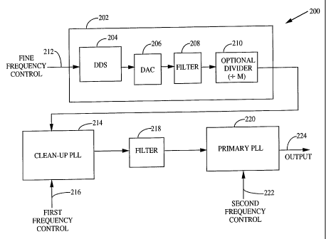
FIG. 2 illustrates an exemplary embodiment of a DDS driven PLL
frequency synthesizer 200. The synthesizer 200 comprises a digital frequency
synthesizer 202, a first or clean-up PLL 214, and a second or primary PLL 220.
Additional filters well known in the art may be added as required by the
particular design.
Digital frequency synthesizer 202 is comprised of direct digital
synthesizer (DDS) 204, digital to analog converter (DAC) 206, filter 208 and
an optional divider 210. Digital synthesizer 202 serves as a variable
CA 02215376 1997-09-15
WO 96!28890 9 PCTliTS96/02559
reference source means for generating a selected one of a plurality of
reference frequency signals, each at a different frequency.
DDS 204 provides an output signal indicative of the digital
representation of a periodic waveform. The components and operation of
DDS 204 are similar to DDS 102 in FIG. 1. DDS 204 is responsive to a fine
frequency control signal 212 capable of altering the frequency of the output
reference signal. DDS 204 is further responsive to a direct digital
synthesizer
(DDS) clock signal with which its internal digital hardware is driven. The
direct digital synthesizer is well known in the art.
~ DAC 206, coupled to DDS 204, converts the digital representation of
the periodic waveform output by DDS 204 into an analog representation of
the waveform. The digital to analog conversion performed by DAC 206
substantially reduces quantization errors present on the output signal of
DDS 204.
Filter 208, coupled to DAC 206, typically reduces wideband noise
present on the DAC 206 output signal. The noise eliminated by filter 208 is
normally outside the bandwidth of subsequent first PLL 214 or second PLL
220. Optionally, the output from filter 208 is provided to a reference
frequency divider 210 having a divisor value M. The resulting periodic
output frequency and noise surrounding the signal, if processed by optional
frequency divider 210, is stepped down in proportion to a predetermined
integer value M.
The output reference signal provided by synthesizer 202, either filter
208 or optional frequency divider 210, is provided to the input of clean-up
PLL 214. Unlike PLL 114, in FIG. 1, the primary function of clean-up PLL 214
is to serve as a lowpass filter that can track a range of phase continuos
input
frequencies, such as those generated by frequency synthesizer 202. Given a
phase continuous variable frequency input signal, clean-up PLL 214
provides a spectrally pure output frequency while maintaining frequency
and phase lock. In an exemplary embodiment, substantially small frequency
multiplication is performed by clean-up PLL 214.
The components and operation of PLL 214 are similar to PLL 114 in
FIG. 1 with two exceptions: the PLL loop divider value and the PLL loop
bandwidth. The loop divider value, indicated by the value N in PLL 114 of
FIG. 1, of clean-up PLL 214 is intentionally set to a small value
substantially
near unity since the frequency multiplication function is performed
primarily by a primary PLL 220. The clean- up PLL 214 loop divider value is
set in response to a first frequency control signal 216. In an exemplary
CA 02215376 1997-09-15
WO 96/28890 1o PCT/US96/02559
embodiment, the output from clean-up PLL 214 produces a spectrally pure
reference signal at a frequency substantially near its input frequency.
Clean-up PLL 214 typically is designed with a small or narrow loop
bandwidth. The size of the loop bandwidth is selected sufficiently small in
order to filter out substantially all close-in noise around the carrier
frequency created by the frequency signal synthesizer 202 or more specifically
DDS 204. In comparison, the clean-up PLL has a significantly smaller loop
bandwidth than a conventional synthesizer's PLL, such as PLL 114 found in
synthesizer 100 in FIG. 1. The difference in bandwidth accounts for the
increased spectral purity available to synthesizers using a clean-up PLL. The
single PLL used in conventional synthesizers, such as PLL 114 in FIG. 1, do
not typically have an arbitrarily small loop bandwidth because they would
suffer an arbitrarily large increase in settling time.
The output signal of clean-up PLL -214 may be coupled through
additional filter 218 before being input to primary PLL 220. Filter 218 serves
as a means for further .increasing the spectral purity of the enhanced
reference signal output by PLL 214. An exemplary filter 218 may be either a
lowpass filter (LPF) or a bandpass filter (BPF) as is well known in the art.
The output of filter 218 is coupled to a second or primary PLL 220.
Generally, PLL 220 is used as a frequency tuning means for generating a loop
output signal having a periodic frequency which is an integer multiple of
the frequency of the input reference signal. In this particular embodiment,
primary PLL 220 steps-up, or multiplies, a signal having frequency generated
by DDS 202 and close-in spectral purity provided by clean-up PLL 214.
The components of PLL 220 are similar to the components of clean-up
PLL 214 with two exceptions. Primary PLL 220 has a much larger loop
divisor and a much larger loop bandwidth than clean-up PLL 216.
The range of loop divider values in primary PLL 220 differ from the
range of loop divider values in clean-up PLL 214. In clean-up PLL 214, the
loop divider value is set to near unity to create a narrow loop bandwidth
and produce a output signal with high spectral purity. Clean-up PLL 214 is
used primarily as a filter means and not a frequency multiplication means.
Primary PLL 220, however, requires a loop divisor value which is much
larger than unity in order to step up the input frequency to the higher
desired output frequency. The primary PLL in the preferred embodiment is
used primarily as a frequency multiplication means and not as a filter
means.
CA 02215376 1997-09-15
WO 96/28890 11 PCTIUS96/02559
In the preferred embodiment, a higher frequency multiplication may
be achieved by setting a larger primary PLL loop divisor value. Generally, a
PLL will increase noise as well as step up frequency in proportion to the loop
divisor value. This factor could limit the signal frequency multiplication
(i.e. size of the loop divisor value) in a conventional synthesizer because
the
amount of noise in the system may reach intolerable levels. However, in
the preferred embodiment a large loop divisor does not greatly enhance
noise because the clean-up PLL provides a reference signal which is
spectrally pure.
The loop bandwidth of PLL 220 may be set arbitrarily large because
sufficient close-in noise is reduced by clean-up PLL 216. Primary PLL 222 is
designed to perform frequency multiplication and relies on clean-up PLL 214
for enhancing spectral purity of the input signal. Generally, a PLL having a
large loop bandwidth will have a much faster settling time (i.e. the time it
takes for the PLL to "lock" onto a new frequency) than a similar PLL having
a smaller loop bandwidth, such as clean-up PLL 214 or primary PLL 114 in
FIG. 1. Specifically, a substantially larger loop bandwidth used by the
primary PLL of the present invention provides significantly faster settling
times than a similar primary PLL, such as PLL 114 used in synthesizer 100 in
FIG. 1, having a smaller loop bandwidth. As a result, the present invention
will have an overall faster settling time than conventional frequency
synthesizer.
In operation, the DDS produces digitized periodic waveforms,
typically sine waves, of a given frequency by accumulating phase values at a
higher rate than the sine wave frequency. The accumulated phase is
translated to a periodic waveform via a lookup table. The resulting digital
representation of the periodic waveform is translated to analog form using a
digital to analog converter.
The spurious performance of the preferred embodiment of the
present invention is readily analyzed. The DDS output includes spurious
signals typically caused by phase truncation of the output waveform,
amplitude quantization of the waveform, nonlinearities of the DAC output,
and aliases attributable to the sampling process. The phase noise in the DDS
is governed by the phase noise characteristics of the DDS clock signal, as
well
as the noise performance of the digital circuitry comprising the DDS.
Clean-up PLL 214 filters out close-in frequency spurs in the signal
generated by DDS 202. By designing clean-up PLL 214 with a very narrow
loop bandwidth the typical harmonic family of spurs are drastically reduced
CA 02215376 1997-09-15
WO 96/28890 12 PCT/L1S96/02559
and a spectrally pure frequency signal is generated by clean-up PLL 214. For
additional details and examples on the effect of the PLL loop bandwidth
reducing spurs from a DDS reference signal see U.S. Patent No. 4,965,533
referenced above.
A clean-up PLL will remain in lock and require little settling time if
the reference frequency signal generated by DDS 202 does not vary beyond
0 f p~ shown in equation (1). The clean-up PLL 214 settling time consists
only of the time delay for phase acquisition when frequency and phase lock
are maintained. Adding a clean-up PLL 214 which remains in lock does not
- contribute substantially to the overall settling time of the synthesizer and
adds, as will be seen, an additional degree of flexibility to the settling
time
equation. The following relationship describes the maximum change in
frequency a PLL comprising either a digital phase or frequency detector, such
as phase detector 116 in FIG. 1, can accommodate before "pulling out" of
frequency lock:
Ofpo - 1.8(20(8+1)f,~ (1)
where:
Of po is the pullout frequency
is the loop damping factor; and
f" is the PLL natural frequency
Even when the reference frequency does vary greater than 0 f po the
overall settling time for synthesizer 200 is improved using clean-up PLL 214
in conjunction with primary PLL 220. Clean-up PLL 214 has a small loop
divisor value and thus PLL 214 output frequency range is roughly equal to
the output bandwidth of DDS 204. In addition, clean-up PLL 214 has a very
small loop bandwidth. Typically, a small loop bandwidth corresponds to a
long frequency settling time. In clean-up PLL 214, however, because
frequency changes are limited, the corresponding times to settle, if any,
remain small. Therefore, even if clean-up PLL 214 breaks lock and must
reacquire the signal, the time delay attributed to phase and frequency
3Q acquisition remains small.
In comparison, when synthesizer 100, shown in FIG. 1, must break
lock and reacquire the reference signal produced by DDS 102 the overall
frequency time delay will remain significantly larger. Given the same
narrow loop bandwidth as PLL 214 in FIG. 2, PLL 114 in FIG. 1-utilizes a
much larger loop divisor to produce an order of magnitude wider frequency
CA 02215376 1997-09-15
WO 96!28890 13 PCT/US96/02559
range. When PLL 114 changes frequency the settling time can not be
improved by increasing the loop bandwidth unless the designer is willing to
sacrifice spectral purity. Therefore, settling time for a PLL to make large
frequency changes takes longer than the settling time for a PLL to make
small frequency changes when the loop bandwidth remains constant.
The preferred embodiment exemplified in synthesizer 200, in FIG. 2,
decreases settling time in the primary PLL 220 by increasing the loop
bandwidth as needed. Now when primary PLL 220 breaks lock the large
loop bandwidth markedly improves the settling time and justifies any
added complexity or costs involved with adding clean-up PLL 214. The
increased settling time achieved in primary PLL 220 more than compensates
for any settling time lost even when clean-up PLL 214 may break lock.
Using clean-up PLL 214 to produce a signal with high spectral purity
adds a degree of freedom in the settling time equation. Primary PLL 220 can
have a relatively large loop bandwidth, in comparison to conventional
primary PLL devices, because the spurs on the incoming reference signal
have been greatly reduced by the clean-up PLL. The large loop bandwidth
used in combination by a large loop divisor in primary PLL 220, allows
frequency synthesizer 200 to acquire signal lock quickly over a large
frequency range. The additional degree of flexibility in the settling time
equation provides a means for improved synthesizer design previously
unavailable.
In practice, a conventional DDS driven PLL synthesizer design will
compromise settling time in exchange for higher spectral purity. Therefore,
a brief comparison between the settling times of the conventional
synthesizer with the preferred embodiment with will make clear the overall
benefit. For example, consider conventional DDS driven PLL synthesizer
100 in FIG. 1 where the DDS portion produces a reference frequency of 1
MHz, the primary PLL 114 loop divisor is equal to 1000 and O f p" = 25 kHz.
The typical settling time, attributed primarily to the primary PLL, for this
synthesizer will be approximately 5 msec. for a 25 MHz jump.
In the preferred embodiment, "clean-up" PLL 214, in FIG. 2, has a
narrow loop bandwidth at least as narrow as primary PLL 114, in FIG. 1. In
addition primary PLL 220 in FIG. 2 has a loop bandwidth significantly larger
than the primary PLL 114 of FIG. 1. Consider the case of DDS driven PLL
frequency synthesizer 200 where the DDS portion produces a reference
frequency of 1 MHz, the clean-up PLL loop divisor is unity, the primary PLL
loop divisor is equal to 1000 and ~ f~,~, = 25 kHz for both PLLs. In this
case,
CA 02215376 1997-09-15
WO 96128890 14 PCT/US96l02559
the settling time for this synthesizer is only approximately 2 msec. for a
25 MHz jump. The larger loop bandwidth of primary PLL 220 in the
preferred embodiment significantly improves frequency settling time over
conventional synthesizers having a primary PLL with a smaller loop
bandwidth. As previously mentioned, the clean-up PLL would contribute a
small delay to the overall settling time even if the frequency step size were
A
to exceed O f p~, and the clean-up PLL were to break lock.
A DDS driven PLL frequency synthesizer having an additional clean
up PLL can be configured several ways to take advantage of the additional
degree of flexibility in the settling time equation. In the first exemplary
configuration of the embodiment, the loop divisor of the primary PLL is set
to a predetermined value in response to a second frequency control signal
222. Clean-up PLL 214, as shown in FIG. 2, has a loop divider value, set by
first frequency control 216, equal to 1 and a substantially small loop
bandwidth. In the alternative, clean-up PLL need not include a loop divider
and the output of its VCO coupled directly back to an input of its phase
detector. The primary PLL 220 in FIG. 2 coupled to clean-up PLL 214 may
have a large loop divisor, set by second frequency control 222, fixed at 1000
and a loop bandwidth much larger than clean-up PLL 214. A reference
frequency of 1 MHz provided by DDS 202, responsive to fine frequency
control 212, can be adjusted up or down 25 kHz around the reference
frequency. The resulting synthesizer, in this case, will have high spectral
purity, due to the narrow loop bandwidth of PLL 214 and unity loop divisor,
as well as fast frequency switching times, due to the large loop bandwidth of
primary PLL 224. However, the frequency output range, obtained by
multiplying the input reference frequency by the primary PLL loop divisor,
will be fixed at 50 MHz.
A second configuration of the invention improves the frequency
range by varying, rather than fixing, the loop divisor value in primary PLL
220. As before, clean-up PLL 214 has a loop divider value substantially equal
to 1 and a relatively small loop bandwidth. The corresponding primary PLL
224, also has a large loop bandwidth but now includes a variable loop
divisor. For example, frequency control 222 may be used to vary primary
PLL loop divisor from 100 to 200. A reference frequency of 5 MHz provided
by DDS 202 is responsive to fine frequency control 212 used to adjust up or
do~n~n 25 kHz around the reference frequency. As previously discussed, the
resulting synthesizer will have high spectral purity, due to the narrow loop
bandwidth and unity loop divisor of PLL 214, as well as fast frequency
CA 02215376 1997-09-15
WO 96/28890 15 PCTlUS96/02559
switching times, due to the large loop bandwidth of primary PLL 224. Now,
however this embodiment will function over a broader range of frequencies
dictated by dynamically setting the primary loop divisor. The output
frequency range from 500 MHz to 1 GHz and will have an average settling
time of approximately 2 msec.
The variable loop divisor configuration may also have an output
signal with fine frequency resolution capabilities. The primary loop divisor
is used as a coarse frequency control while the DDS frequency control is used
selected all the frequencies in between. Generally, the resolution of the
output frequency is proportional to the DDS frequency resolution times the
current loop divisor value. A typical DDS having a 32 bit accumulator will
produce an output frequency having a 0.93 Hz resolution when the
primarily PLL loop divisor is 200. Lower- loop divisor values will enable
even finer frequency resolution adjustments. When the PLL loop divisor is
set to 100 the frequency resolution is increased to 0.465 Hz.
FIG. 3 illustrates in block diagram form an alternate embodiment of
the present invention utilizing a clean-up PLL 318 to obviate the need for
various components. In FIG. 3, synthesizer 300 includes a frequency
synthesizer 302, a clean-up PLL 318 and a primary PLL 324.
In this embodiment, synthesizer 302 comprises a DDS 304, a filter 314
and an optional divider 316. Of particular interest is that DDS 304 may only
require phase accumulator 306 to operate if a clean-up PLL is also utilized. A
sine lookup table, such as sine lookup table 106 in FIG. 1, and a digital to
analog converter (DAC), such as DAC 108 in FIG. 1, are not needed in this
implementation. Phase accumulator 306 receives a digital fine frequency
control signal which determines the phase increment for accumulation at
the DDS clock rate. A most significant bit (MSB) or overflow bit 310 passes
through filter 314 and optional divider means 316 before being provided to
clean-up PLL 318.
MSB 310 is coupled, through either filter 314 or optional divider 316,
to a clean-up PLL 318 having similar components and operation as clean-up
PLL 214 in FIG. The input signal generated by MSB 310 clearly indicates
when the amplitude of the synthesized periodic signal has changed
inflection despite possible distortion in the actual sinusoidal wave. The
phase detector in PLL 318 is responsive to changes in MSB 310. Effectively,
clean-up PLL 318 receives the input signal generated by MSB 310 and
perceives a "square wave" or truncated sinusoidal. Phase errors that may be
present, are inherently corrected by the narrow bandwidth of the clean-up
CA 02215376 1997-09-15
WO 96128890 PCTlL1S96/02559
16
PLL 318. The resulting output signal from clean-up PLL 318 appears to be a
sine wave.
The output from clean-up PLL 318 is coupled to a primary PLL 324
and may have a filter 322 located therebetween. Primary PLL 324 is used as a
frequency tuning means for generating a ' loop output signal having a
periodic frequency- which is an integer multiple of the frequency of the input
reference signal. The components and operation of primary PLL 324 are ''
similar to those of primary PLL 214 illustrated in FIG. 2.
Clean-up PLL 318 effectively produces what appears to be a sine wave
signal using only MSB 310. The sine wave produced by clean-up PLL 318 is
sufficient to drive the phase detector in primary PLL 324. Therefore, this
embodiment obviates the need for sine look-up table, such as sine took up
table 106 in FIG. 1, and digital to analog converter, such as digital to
analog
converter 108 in FIG. 1. Utilizing a reference signal generated by MSB 306_ in
combination with clean-up PLL 318 has the advantages of lower costs and
reduced complexity.
FIG. 4 illustrates in block diagram form yet another alternate
embodiment wherein a DDS driven PLL frequency synthesizer with a clean-
up PLL used in combination with a switching apparatus can be used to
further improve overall settling time when switching frequencies. In FIG.
4, frequency synthesizer 400 includes a DDS 402, a digital to analog converter
(DAC) 404, a filter means 406, a power splitter 408, a clean-up PLL filter
410,
switch SW1 414, switch SW2 412 , a switching control means 416, a summer
418 and primary PLL 420.
Direct digital synthesizer (DDS) 402 serves as a variable reference
source means for generating a selected one of a plurality of reference
frequency signals. The operation and components of DDS 402 are similar to
DDS 204 as illustrated in FIG. 2. The output of DDS 402 is coupled with DAC
404 whose operation is also similar to DAC 206 also in FIG. 2.
Spectral purity of signal produced by DDS 402 may optionally be
enhanced utilizing filter 406. The output from DAC 404 is coupled to filter
406 to reduce wide band noise and also improve signal quality when clean-
up PLL 410 may not be engaged.
The output of DAC 404 or optionally filter 406 is coupled to the input
of a power sputter 408 which distributes the signal into two separate
branches. The output of the first branch from sputter means 408 is coupled
to a clean-up PLL 410. The operation and components of clean-up PLL 410
are similar to clean-up PLL 214 as illustrated in FIG. 2. A switch 414 is
CA 02215376 1997-09-15
WO 96!28890 17 PCT/US96/02559
responsive to a switching control means 416 and receives the output from
clean-up PLL 410. The resulting output from switch 414 is coupled to one
input of summer 418.
The output of the second branch from splitter means 408 is coupled to
switch 412. The output from switch ~ SW2 412 is then also coupled to a
second input of summer 418. The output from summer 418 is then
provided to primary PLL 420.
This embodiment describes a switching technique to further reduce
the settling time of the present invention when switching frequencies.
Prior to switching frequencies, switching control means 416 will close switch
412 and open 414. After the frequency is changed, switching control means
416 will delay a predetermined time necessary for clean-up PLL 410 to lock
onto the new frequency. Once clean-up PLL 410 has settled onto the new
frequency, switching control means will close switch 414 and then open
switch 412. Preferably, a make before break technique- is used between
switches SW1 414 and SW2 412 to minimize switching noise and signal
discontinuities.
Primarily, this switching technique reduces any settling time which
may be introduced by a clean-up PLL by bypassing PLL 410. In this
embodiment, the overall frequency switching time will be limited to only
the settling time of primary PLL 420. It should be noted that while switch
414 remains open and switch 412 closed, spurious signals may be output
from summer 418 and into primary PLL 420. Typically, the spurious signals
that are transmitted are confined to the loop bandwidth of primary PLL 420
and are of minimal duration.
The previous description of the preferred embodiments is provided
to enable any person skilled in the art to make or use the present invention.
The various modifications to these embodiments will be readily apparent to
those skilled in the art, and the generic principles defined herein may be
applied to other embodiments without the use of the inventive faculty.
Thus, the present invention is not intended to be limited to the
embodiments shown herein but is to be accorded the widest scope consistent
with the principles and novel features disclosed herein.
I CLAIM: