Note: Descriptions are shown in the official language in which they were submitted.
CA 02215506 2007-05-22
= WO 96/30771 PGT/US96/03583
NARROW FIELD ELECTROMAGNETIC
SENSOR SYSTENi' AND METHOD
The United States Govemment has rights in this invention
pursuant to Contract Number W-7405-ENG-48 between the United
States Department of Energy and the University of California for the
operation of Lawrence Livermore National Laboratory.
Continuing Application Data
This application is a continuation-in-part of U.S. Patent No. 5,510,800
titled "Time-of-Flight Radio Location System ".
BACKGROUND OF THE INVENTION
Field of the Invention 15 The present invention relates to electronic sensors,
and more
particuiarly to sensors utilizing ultra-wideband transmitters and receivers
in narrow field applications.
Descrjption of Related Art
One type of narrow ield sensor can be referred to as a "trip wire.'* A
mechanical "trip wire" detects motion in or through a narrow field when
pressure is applied to a trip wire placed across a path in the narrow field.
Non-mechanical "trip wires," such as those formed with electromagnetic
radiation or ultrasound, also exist. Laser, infrared, and ultrasound "trip
wires" detect motion in or through a narrow field by sensing a disruption
in the narrow field across a path. Some examples of "trip wire"
applications include using it for game trapping, conveyor belt counting,
people counting, and safety sensing for automatic doors_ Thus, a "trip
-1-
CA 02215506 1997-09-16
WO 96/30771 PCT/US96/03583
wire" sensor can be used to activate a net for trapping game, to count
objects on a conveyor belt, count people at a doorway entrance, or to
prevent an open automatic door from closing when people are in the
vicinity of the doorway.
Common electronic narrow field sensors are based on laser,
ultrasound, or infrared techniques. Laser or infrared beam-interruption
sensors can be focused in a narrow field. However, visibility between
the two ends of the field is required and anything that affects this
visibility may impair the sensor. Thus, interference from sunlight, dirt, or
snow prevents the proper operation of this sensor. Infrared sensors
also have no range adjustments. Similarly, optical and ultrasound
sensors suffer from blockage by dirt, rain, snow, or any other material.
Sunlight will also provide harmful interference for optical sensors.
The transducers in optical, ultrasound, and magnetic sensors are
also expensive to manufacture and thus, make them less attractive for
commercial purposes. Other sensors are also not commercially feasible
because they drain too much power.
FM-CW and Doppler radar sensors, which might be applied as
trip wires, also suffer limitations: low material penetration due to the
higher frequencies employed, microphonics caused by the use of short
radar wavelengths combined with audio frequency processing,
frequency crowding, and poor short-range operation.
Although directional antennas with narrow beamwidths may
provide an adequately narrow field or trip wire, they are too expensive in
a compact package. Furthermore, at some frequencies, narrow
beamwidths are almost impossible to produce in a compact antenna
without increasing its complexity. The low frequency microwave band is
-2-
SUBSTITUTE SHEET (RULE 26)
CA 02215506 1997-09-16
WO 96/30771 PCT/US96/03553
one example. Thus, at this band, material penetration is available but a
compact and practically available narrow beamwidth antenna is not.
Another limitation of these sensors is that, for image processing
applications, certain characteristics of the object cannot be obtained.
= 5 For example, the thickness or density of an object at any desired region
of the object cannot be determined.
An effective and commercially practical sensor should be
inexpensive to manufacture, drain as little power as possible, last a long
time, and be durable and impervious to harsh environmental conditions
such as dirt, rain, snow, and sunlight. Furthermore, sensors should be
able to use signals that can penetrate certain material without damaging
the material. Such material penetration allows users to install these
sensors behind wood, concrete, or other objects for security purposes
and still permit the sensor to function. The compact size of sensors is
also desirable to reduce cost, reduce complexity, and provide.ease of
installation. In other applications, motion sensors that are insensitive to
movement of the sensors themselves are particularly valuable when
these sensors are placed on moving objects.
SUMMARY OF THE INVENTION
The present invention is a cost-effective, low power, and long-
lasting electronic sensor that is impervious to harsh environmental
conditions such as dirt, rain; snow, and sunlight. Furthermore, the
sensor of the present invention uses signals that can penetrate certain
materials (without damaging the material) to allow users to install them
behind wood, concrete, or other objects for security purposes. The
sensor can also be placed on a moving object without impairing its
-3-
SUBSTITUTE SHEET (RULE 26)
CA 02215506 1997-09-16
WO 96/30771 PCT/US96/03583
performance. The sensor can be used for electronic trip wire and image
processing applications.
The present invention can be characterized as a narrow field =
electromagnetic sensor, comprising a transmitter, a receiver, a timing
circuit, and a signal processor. The transmitter transmits a sequence of
electromagnetic signals in response to a transmit timing signal. The
receiver samples the sequence of electromagnetic signals in response
to a receive timing signal and generates a sampled signal. The timing
circuit supplies the transmit timing signal to the transmitter and the
receive timing signal to the receiver, where the receive timing signal
causes the receiver to sample a portion of each electromagnetic signal
that travels along a direct RF path between the transmitter and the
receiver. The signal processor coupled to the output of the receiver and
responsive to the sampled signal provides an indication of a
characteristic, such as presence in the narrow field or density, of the
object.
The sensor can also include a phase modulator for modulating
the receive timing signal into a plurality of phase states for sampling the
sequence of electromagnetic signals. The phase modulator includes a
quadrature-phase modulator providing four phase states of about 0
degrees, about 90 degrees, about 180 degrees, and about 270 degrees.
Based on the phase modulator, the receiver changes phase states
sequentially at a frequency of about 500 Hz. In other embodiments, the
phase states change at a frequency between 10 Hz and 100 KHz.
In some embodiments, the electromagnetic signal is an RF pulse
providing a wide band signal or a short burst of several cycles to provide
a narrower band signal. The transmitter of the present invention which
generates the electromagnetic signal further comprises a line receiver,
-4-
SUBSTITUTE SHEET (RULE 26)
CA 02215506 1997-09-16
WO 96/30771 PCTIUS96/03583
a transmitter pulse forming network, and a pulsed transmitter RF switch
or oscillator. The line receiver shapes the transmit timing signal. The
transmitter pulse forming network coupled to the output of the line
receiver and responsive to the amplified transmit timing signal generates
= 5 a transmitter pulse. The pulsed transmitter RF switch or oscillator
coupled to the output of the transmitter pulse forming network and
responsive to the transmitter pulse forms the electromagnetic signal.
The receiver of the present invention further comprises a receiver
pulse forming network, a pulsed receiver switch or RF oscillator, and a
sampling circuit. The receiver pulse forming network coupled to the
output of the timing circuit and responsive to the receive timing signal
forms a receiver pulse. The pulsed receiver switch or RF oscillator
coupled to the output of the pulse forming network and responsive to the
receiver pulse forms a receiver gating signal. The sampling circuit
coupled to the output of the pulsed receiver RF oscillator and responsive
to the receive gating signal and the electromagnetic signal forms a
sampled signal.
The signal processor of the present invention comprises a band
limited amplifier, a peak detector, and a comparator. The amplifier is
bandlimited to provide coherent integration of a large number (e.g., 10-
10,000) of received and sampled RF pulses. The amplifier coupled to
the output of the sampling circuit and responsive to the sampled signal
generates an amplified sampled signal. The peak detector coupled to
the output of the amplifier and responsive to the amplified sampled
signal generates a peak detected signal which is an indication of a
characteristic of the object. The comparator is coupled to the output of
' the peak detector and responsive to the peak detected signal and a
predetermined reference signal. The comparator generates an eclipse
-5-
SUBSTITUTE SHEET (RULE 26)
CA 02215506 1997-09-16
WO 96/30771 PCT/US96/03583
indication when the peak detected signal is less than the reference
signal.
In other embodiments, a noise generator can be coupled to the
input of the timing circuit for providing random variations to the timing
circuit. This reduces interference among co-located sensors because it
is unlikely that two sensors will simultaneously transmit and sample the
pulses.
In another embodiment of the present invention, the sensor can
be mounted with a scanner to obtain a multidimensional characteristic of
the object. The scanner comprises a translation stage and a processor
and storage unit. The translation stage mounts the transmitter and the
receiver and moves the transmitter and the receiver with respect to the
object. The processor and storage unit coupled to the signal processor
and responsive to the sampied signal stores a coordinate position on the
object and the magnitude of the sampled signal at each coordinate
position.
The present invention can also be characterized as an electronic
trip wire. The electronic trip wire comprises a transmitter, a receiver, a
timing circuit, and an eclipse indicating circuit. The transmitter,
responsive to a transmit timing sigrial, generates a sequence of RF
pulses or bursts. The receiver responsive to a receive timing signal
samples a portion of each RF burst and generates a sampled receive
signal. The timing circuit provides the transmit timing signal to the
transmitter and the receive timing signal to the receiver so that the
receiver samples only a portion of each RF burst that corresponds to a
direct RF path of the RF pulse or burst between the transmitter and the
receiver. The eclipse indicating circuit coupled to the output of the receiver
and responsive to the sampled receive signal provides an
-6-
SUBSTITUTE SHEET (RULE 26)
CA 02215506 1997-09-16
WO 96/30771 PCT/1JS96/03583
eclipse indication when an object obstructs the path of the RF pulse or
burst along the direct RF path. Furthermore, the electronic trip wire
includes a pulse repetition frequency generator coupled to the input of
the timing circuit for providing a clock signal. In one example, the
= 5 frequency of the clock signal is about 2 MHz.
The timing circuit of the present invention comprises a phase
modulator coupled to the output of the pulse repetition frequency
generator and responsive to the clock signal for generating a receive
timing signal that sequentially moves among a plurality of phase states
to sample the RF pulse or burst traveling along the direct RF path. The
timing circuit includes a delay circuit which compensates for the direct
RF path time-of-flight distance between the transmitter and the receiver
so that the receiver samples a portion of the RF burst travelling along
the direct RF path. The transmitter and receiver of the present invention
are analogous to those of the sensor as described above.
The eclipse indicating circuit of the present invention comprises a
peak detector and a comparator. The peak detector responsive to the
sampled receive signal provides a peak detected signal. The
comparator coupled to the outpui of the peak detector and responsive to
the peak detected signal and an adjustable referznce signal provides an
eclipse indication when the peak detected signal is less than the
reference signal.
The present invention can be characterized as a method of
sensing a characteristic of an object, comprising the steps: providing a
common clock signal; deriving a transmit timing signal and a receive
timing signal from the common clock signal, the receive timing signal
' adjusted so that sampling of the electromagnetic signal coincides with
the arrival of the electromagnetic signal corresponding to the direct RF
-7-
SUBSTITUTE SHEET (RULE 26)
CA 02215506 2007-05-22
path; transmitting a sequence of electromagnetic signals in response to
the transmit timing signal; receiving each electromagnetic signal in
response to the receive timing signal to provide a sampled signal; and
providing an indication of a characteristic of the object from the
magnitude of the sampled signal.
The step of transniitting a sequence of electromagnetic signals
further comprises forming a transmit pulse in response to the transmit
timing signal, and forming an electromagnetic signal in response to the
transmit pulse. The step of receiving the electromagnetic signal further
comprises forming a receiver pulse in response to the receive timing
signal, forming a receive gating signal in response to the receiver pulse
that samples only the direct RF path portion of the electromagnetic
signal, and forming a sampled signal in response to the receive gating
signal and the electromagnetic signal.
Additional steps in other embodiments include comparing the
magnitude of the sampled signal with the magnitude of an adjustable
reference signal; and providing a trip indication when the magnitude of
the sampled signal is less than the magnitude of the adjustable
reference signal. Other embodiments include noise dithering the
common clock signal to reduce interference among co-located sensors.
Another embodiment includes the step of phase modulating the
clock signal to provide a receive timing signal sothat sampling the
electromagnetic signal occurs at one of a plurality of phase states, each
phase state measured from the leading edge of the direct RF path
electromaqnetic siqnal.
-8-
CA 02215506 2008-03-28
According to an aspect of the present invention there is provided a direct
radio frequency path electromagnetic sensor, comprising:
a transmitter which transmits a sequence of electromagnetic signals in
response to a transmit timing signal;
a receiver which samples the sequence of electromagnetic signals in response
to a receive timing signal, and generates a sampled signal;
a timing circuit which supplies the transmit timing signal to the transmitter
and
the receive timing signal to the receiver, the receive timing signal gating
the
receiver to sample a portion of each electromagnetic signal that travels along
a
direct radio frequency path between the transmitter and the receiver and to
reject
multipath signals; and
a signal processor coupled to the output of the receiver and responsive to the
sampled signal to provide an indication of a characteristic of an object to be
sensed.
According to another aspect of the present invention there is provided an
electronic trip wire, comprising:
a transmitter responsive to a transmit timing signal for generating a sequence
of
radio frequency bursts;
a receiver responsive to a receive timing signal for sampling a portion of
each
radio frequency burst, and for generating a sampled receive signal;
a timing circuit for providing the transmit timing signal to the transmitter
and the
receive timing signal to the receiver so that the receiver is gated to sample
a
portion of each radio frequency burst that corresponds to a direct radio
frequency
path of the radio frequency burst between the transmitter and the receiver and
to
reject multipath signals; and
an eclipse indicating circuit coupled to the output of the receiver and
responsive
to the sampled receive signal for providing an eclipse indication when an
object
obstructs the path of the radio frequency burst along the direct radio
frequency
path.
According to a further aspect of the present invention there is provided a
method of sensing a characteristic of an object, comprising:
providing a common clock signal at a nominal frequency;
deriving a transmit timing signal and a receive timing signal from the common
-8a-
CA 02215506 2008-03-28
clock signal, the receive timing signal adjusted so that sampling of a
electromagnetic signal coincides with the arrival of the electromagnetic
signal
corresponding to a direct radio frequency path;
transmitting a sequence of electromagnetic signals in response to the transmit
timing signal;
receiving each electromagnetic signal in response to the receive timing signal
to
provide a sampled signal, wherein direct path signals are gated and multipath
signals are rejected; and
providing an indication of a characteristic of the object from the magnitude
of
the sampled signal.
Other aspects and advantages of the present invention can be
ascertained upon review of the figures, the detailed description, and the
claims
which follow.
-8b-
CA 02215506 1997-09-16
WO 96/30771 PCT/US96/03583
BRIEF DESCRIPTION OF THE DRAWINGS
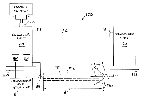
FIG. 1 is a simplified block diagram showing an embodiment of
the present invention.
FIG. 2 is a simplified model of the sensor region and the trip
region in accordance with the present invention.
FIG. 3 is a simplified block diagram showing more details of the
receiver and the transmitter according to the present invention.
FIG. 4 shows an illustrative plot of the direct path and indirect
path RF waveform with respect to time.
FIG. 5 shows an illustrative plot of the RF waveform with respect
to time and the eclipsed signal when an object obstructs the trip region
in accordance with the present invention.
FIG. 6 shows an illustrative plot of the timing of the receiver
gating, or sampling, signal which coincides with the eclipsed RF signal
in accordance with the present invention.
FIG. 7 shows an illustrative plot of the voltage output of the peak
detector with respect to distance across the trip region as an object
-20 passes across the trip region in accordance with tfie present invention.
FIG. 8 shows an illustrative plot of the voltage output of the peak
detector when Biphase modulation is used.
FIG. 9 shows an illustrative plot of the voltage output of the peak
detector when Quadrature-phase modulation is used in accordance with
the present invention.
FIG. 10 is a circuit diagram of the receiver of an embodiment of
the present invention.
-9-
SUBSTITUTE SHEET (RULE 26)
CA 02215506 1997-09-16
WO 96/30771 PCT/US96/03583
FIG. 11 is a circuit diagram of the transmitter of an embodiment
of the present invention.
FIG. 12 is a block diagram of another embodiment of the present
invention, where computer-aided scanning techniques are used to
obtain a three-dimensional characteristic of the object.
DETAILED DESCRIPTION OF PREFERRED EMBODIMENTS
The embodiments of the present invention have a wide variety of
applications ranging from image processing to electronic trip wires. The
sensor of the present invention uses time-of-flight techniques to
precisely determine the range between the transmitter and the receiver.
With the set range, the sensor can exclude all but the direct path
propagation wave of the transmitted electromagnetic signal. With the
signal processing circuitry employed in the sensor, narrow sensor
regions can be effectively generated even with omni-directional
antennas. The sensor is concealable; as a security device, the sensor
can be installed on either side of a doorway or hallway and detect
passersby from. behind the wood door frame or concrete walls. The
sensor is stealthy; its RF emissions are nearly undetectable. The
sensor is inexpensive to manufacture; its components are inexpensive
and its transducer is a short piece of wire serving as the antenna.
As a safety or industrial sensor, the embodiments of the present
invention can detect the presence of a person or a car in an automatic
doorway, or detect objects on a conveyor belt. The sensor can also be
hermetically sealed against harsh environments; it is impervious to
blockage by dirt, snow, wood, concrete, and rain. The sensor system
also incorporates circuitry for an ultra-wideband spread spectrum
system that reduces interference to and from other RF services while
-10-
SUBSTITUTE SHEET (RULE 26)
CA 02215506 2007-05-22
WO 96/30771 PCT/US96/03583
allowing co-location of multiple electronic sensors without the need for
frequency assignments.
For image processing, the embodiments of the present invention
can be adapted for use with ballistic photon techniques for imaging.
characteristics of an object in a medium. When the medium is air,
electromagnetic radiation travels at the speed of light and the resolution
for irnaging the object is low. When the medium has a higher index of
refraction, such as water, electromagnetic radiation travels at a slower
speed and a higher imaging resolution is possible. The sensor provides
an indication of a characteristic of the object to an imaging processor for
storage and further processing. A complete scan of the object by the
sensor of the present invention provides the imaging processor with an
equivalent image and other characteristics of the object. The frequency
band used in the sensor of the present invention is harmless to all
tissue, particularly mammalian tissue including human tissue.
The embodiments of the present invention utilize time-of-flight
techniques as described in related U.S. Patent No. 5,510,800 titled "Time-of-
Flight Radio Location System." A detailed description of the preferred
embodiments of the present invention is provided with reference to the
figures, in which FIGS. 1, 2. and 3 provide illustrations of the basic
concept.
In FIG. 1, sensor 100 includes a receiver 110, a transmitter 120,
a cable 112 connecting the receiver 110 and the transmitter 120 to each
other, a transmitter antenna 122, and a receiver antenna 113. The
transmitter 120 and receiver 110 use radio frequency (RF) signals to
generate a sensor region 151. The transmitter antenna 122 and the
-?1-
CA 02215506 1997-09-16
WO 96/30771 PCT/1JS96/03583
receiver antenna 113 are each a short piece of wire that radiates signals
omnidirectionally. The distance, d, beiween the transmitter antenna 122
and the receiver antenna 113 is user-defined and fixed for any given =
installation; however, the maximum distance d is limited only by path
losses and other factors that contribute to RF signal degradation.
To couple the transmitter 120 to the receiver 110, one end of the
cable 112 is connected to port 111 of the receiver 110 and the other end
is connected to port 121 of the transmitter 120. The sensor 100
receives power at port 140 of the receiver 110. The receiver 110 and
transmitter 120 are placed on or mounted in objects 160 and 161,
respectively. These objects can be the floor or any support frame in a
wall.
In response to a transmit timing signal, the transmitter 120
transmits an electromagnetic signal 170 via transmitter antenna 122. In
accordance with one embodiment of the present invention, the
electromagnetic signal 170 is a short RF pulse or burst. The receiver
110 receives the electromagnetic signal 170 at receiver antenna 113.
Because of scattering and interference from nearby objects, the receiver
110 receives the aiectromagnetic signal 170 at receiver antenna 113
from multiple paths (direct paths and indirect pa'ths).
FIG. 1 shows a sensor region 152. FIG. 2 shows a more detailed
representation of the sensor region 152. With reference to FIGS. 1 and
2, the sensor region 152 includes a trip region 151. Both regions are
conceptually cylindrical in shape and lie between the transmitter
antenna 122 and the receiver antenna 113. The sensor region 152 has
a radius of rSR and occupies a volume of nrSRZd. The trip region 151 has
a radius of rTR and occupies a narrower volume of nrTRZd. Trip region -12-
SUBSTITUTE SHEET (RULE 26)
CA 02215506 1997-09-16
WO 96/30771 PCT/US96/03583
151 also represents the direct RF path of the electromagnetic signal 170
from the transmitter 120 to the receiver 110.
The cylindrical representation of the sensor region 152 in FIG. 2
is a model. No physical cylinder actually exists. In fact, depending on
= 5 the application and installation, the region between the transmitter
antenna 122 and the receiver antenna 113 may be partially obstructed
by wood, concrete, dirt, or other material. The model merely conveys
the concept that activation of the sensor is possible in a narrow
cylindrical region called the trip region which is also the transmitter-to-
receiver direct RF path of the electromagnetic signal.
When an object moves across the sensor region 152 in a
direction transverse to its length, or distance d, so that the object
impinges the sensor region 152 first and then the trip region 151, the
magnitude of the electromagnetic signal received by the receiver 110
decreases. When the object obstructs, or eclipses, the trip region 151
substantially in its entirety, the eclipse indicator 130 (in FIG. 1) of the
receiver 110 provides an output indicating that the sensor has been
activated. The eclipse indicator 130 provides the signal for further
control, measi:rement, or communication by the sensor. 100.
The magnitude of the electromagnetic signal varies depending on
the number of "ballistic photons" which passes through it, indicating
thickness and density of the object being sensed. Thus, when an object
eclipses the trip region in its entirety, the magnitude of the
electromagnetic signal will be lower for a high density object of a
particular thickness than for an object with lower density of the same
thickness. Based on the electromagnetic signal magnitude for each
coordinate position on the object, a characteristic of the object can be
determined. For example, the density at each coordinate position on the
-13-
SUBSTITUTE SHEET (RULE 26)
CA 02215506 1997-09-16
W O 96/30771 PCT/US96103583
object can be derived from the electromagnetic signal magnitudes.
Sensor output 180 provides the magnitude of the gated electromagnetic
signal. For every voltage reading at 180 when the eclipse indicator 130
is active, a measurement of a characteristic, such as density or
thickness, of an object can be obtained at each coordinate position on =
the object. Processor and Storage Unit 181 provides for storage and
subsequent signal processing of the electromagnetic signal magnitude,
such as for imaging.
When used as an electronic trip wire, the trip region can be used
to indicate the presence of an object along any portion of the trip region.
When the magnitude of the electromagnetic signal is sufficiently low
(below a predetermined threshold), the sensor will provide an eclipse
indication. The eclipse indication signal can be used for further
processing, control, or communication.
FIG. 3 shows a more detailed block diagram of the sensor 200 in
accordance with the present invention. Power is supplied to the sensor
200 via port 203. In this example, a 9 volt source is sufficient. Port 203
is connected to voltage regulator 204 which regulates a substantially
constant V,,p supply of 5 volts in this example.
A pulse repetition frequency (PRF) generator 214 provides a 2
MHz clock signal, or timing signal, for the sensor 200 in this example.
--The 2 MHz timing signal is used by both the transmitter 220 and the
receiver 210. For the transmitter 220, the 2 MHz timing signal is
provided to a line driver 215. A capacitor 216 is connected between the
output of the line driver 215 and node 211. An inductor 217 is coupled
between the power supply and the cable 212 at node 211 to supply
power to the transmitter 220. Both the timing signal and the injected
power are superimposed and delivered to transmitter 220 via cable 212.
-14-
SUBSTITUTE SHEET (RULE 26)
CA 02215506 1997-09-16
WO 96/30771 PCT/US96/03583
The transmitter 220 receives the superimposed power and timing
signal at port 221. The power take-off circuitry includes an inductor 222
connected between port 221 and node 244. A capacitor 223 is
connected between node 244 and ground (GND). The power from this
= 5 power take-off circuit is delivered to all other components of the
transmitter 220. A line receiver 225 receives the timing signal. A
capacitor 224 is connected between port 221 and line receiver 225. The
output of the line receiver 225 is provided to a transmitter pulse forming
network (PFN) 226 that generates a 2 ns pulse to a gated or pulsed 2
GHz transmitter RF oscillator 227, in this example. The gated 2 GHz
transmitter RF oscillator is connected to a quarter-wave (a!4) wire
monopole transmitter antenna 229 via port 228. The transmitter
antenna 229 radiates the electromagnetic signal, a 2 ns RF 'burst, in all
directions.
The sensor region 201 is represented as a cylinder and includes
a cylindrical trip region 202. The trip region 202 is the direct path of the
electromagnetic signal from the transmitter antenna 229 to the receiver
antenna 243.
The timing signal at node 247 generated by the PRF generator
214 is also used by the receiver 210. A Divide-by-N frequency divider
217 receives the timing signal and provides a first phase signal at a
reduced frequency to represent a phase state of 90 degrees at node
219. The first phase signal at node 219 is also provided to a Divide-by-2
frequency divider 218 which generates a second phase signal at half the
frequency of the first phase signal at node 230 to represent a phase
state of 180 degrees from the timing signal. A. quadrature phase
modulator 245 receives the timing signal at node 246, the first phase
signal at node 219, and the second phase signal at node 230. The
-15-
SUBSTITUTE SHEET (RULE 26)
CA 02215506 1997-09-16
WO 96/30771 PCT/US96/03583
output of the quadrature phase modulator 245 is a phase signal that
hops among four phase states of 0 degrees, 90 degrees, 180 degrees,
and 270 degrees. The phase signal hops from one phase state to
another at a frequency of 500 Hz. In other embodiments, the phase
signal hops from one phase state to another at a frequency between 10 =
Hz and 100 KHz. In essence, the phase signal provides additional time
delays (represented by each of the phase states) to a subsequent delay
circuit 231.
The phase signal is provided to a delay circuit 231 which is
adjusted so that, at any one sampling interval, the receiver 210 gates, or
samples, the electromagnetic signal at a phase state from a point near
its leading edge. Without the phase signal, the delay circuit 231 controls
the time at which the receiver 210 samples the arriving electromagnetic
signal from the transmitter 220. Because the distance between the
transmitter 220 and the receiver 210 is fixed, the delay can be readily
calculated. Theoretically, the receiver 210 should sample the arriving
direct RF path electromagnetic signal at its leading edge. However, due
to variations in circuit components and other environmental conditions,
the receiver 210 cannot always sample exactly at the leading edge.
Thus, the delay circuit 231 provides the receiver 210 with a sample point
near the leading edge of the arriving electromagnetic signal. With the
phase signal, the new sample point is located at a point which is a
phase state from the original sample point. Although the overall
sampling occurs at the frequency of the PRF generator 214, the phase
state changes at a slower rate. Thus, in one example, sampling occurs
at 2 MHz but the phase state changes at 500 Hz.
The delayed phase signal is then provided to a receiver pulse
forming network (PFN) 232 which provides a 2 ns pulse to a 2 GHz
-16-
SUBSTITUTE SHEET (RULE 26)
CA 02215506 1997-09-16
WO 96/30771 PCT/US96/03583
pulsed receiver RF oscillator 233. The output of the pulsed receiver RF
oscillator 233 is provided to a samplirig circuit 234. In one embodiment,
the sampling circuit is a single diode sample-and-hold circuit that acts as
a mixer circuit for the RF oscillator and the received electromagnetic
signal at port 242. Adjustments to the delay circuit 231 can be made
such that the receiver PFN 232 pulses the pulsed receiver RF oscillator
233 at the time of arrival of the direct path electromagnetic signal at port
242 from the transmitter 220. Such pulsing results in the gating or
sample-and-holding by sampling circuit 234 of a portion of the
electromagnetic signal located at about the leading edge of the
electromagnetic signal corresponding to the direct RF path and at phase
states modulated at 500 Hz.
At the output of the sampling circuit 234, a holding capacitor 235
is coupled between node 247 and GND. Because the phase signal at
the output of the quadrature-phase modulator 245 hops among the four
phase states at a rate of 500 Hz, the detected electromagnetic signal at
holding capacitor 235 has spectral components at 500 Hz. The
detected electromagnetic signal is amplified by amplifier 236 to produce
an amplified electromagnetic signal. Amplifier 236 is bandlimited to
provide coherent integration of a large number (e.g., 10-10,000) of
received and sampled RF pulses. Peak detector 237 detects the peak
of the amplified electromagnetic signal and produces VPD at node 238.
VPp provides one input to comparator 239. The other input, VREF,
is generated by the common voltage source Voo connected in series to a
variable resistor 240. The lead for VREF is connected to the variable
resistor 240. The comparator 239 compares VPO to VREF. When VP0 ) is
less than VREF, a logic level signal is provided to eclipse indicator 241
indicating that an eclipse has occurred. As discussed above, an eclipse
-17-
SUBSTITUTE SHEET (RULE 26)
CA 02215506 1997-09-16
WO 96/30771 PCT/US96/03583
is an obstruction of the trip region 202 by an object along a direction
transverse to the length of the trip region 202. Thus, when an object
totally eclipses the direct path between the transmitter antenna 229 and
the receiver antenna 243, Vpo decreases to a level below VREF.
Alternatively, a voltage reading from sensor output 250, which
corresponds to VPO, wili indicate a characteristic of ttie object, and can
be stored for subsequent processing. VVhen the entire object is
scanned, a plurality of VPD readings for all coordinate positions of the
object will provide a measure of density, for example, of various points
on the object.
In another embodiment of the present invention, the sensor can
be used as an electronic trip wire. As described above, when an object
totally eclipses the direct patn between the transmitter antenna 229 and
the receiver antenna 243, VPo decreases to a level below VREF. When
VPp is less than VREF, a logic level signal is provided to eclipse indicator
241 indicating that an eclipse has occurred. The logic level on eclipse
indicator 241 provides an indication of whether an object has totally
eclipsed the trip region 202. In other embodiments, a partial eclipse of
the trip region 202 will be sufficient to "trip" the sensor. An adjustment
of VREF will provide various user-selected trip points.
In another embodiment of the present invention, as shown in FIG.
3, the sensor employs randomly or pseudo-randomly dithered PRF
operation. Without noise dithering, the emission spectrum shows
spectral lines at harmonics of the pulse repetition frequency. The
envelope formed by the spectral lines is identical in shape to the
spectrum produced by a single impulse. If either random or code-
generated pseudo-random modulation, or dither, is added, the emission
spectrum can be spread to resemble the shape of a single impulse.
-18-
SUBSTITUTE SHEET (RULE 26)
CA 02215506 1997-09-16
WO 96/30771 PCT/US96/03583
Hence, the peak amplitude is reduced because the energy that was
concentrated in individual lines is spread out. Interference to
conventional receivers is reduced accordingly, and resembles thermal
noise. With noise dithering, multiple and independent sensors 200 may
be co-located without interference with a noise generator 213 coupled to
the PRF generator 214. T f ie noise generator 213 introduces random
variations to the PRF generator 214.
Thus, in FIG. 3, one embodiment of the present invention shows
a sensor having a receiver and a transmitter coupled to the receiver via
a cable for timing and power signals. The transmitter sends
electromagnetic signals via a transmitter antenna and the receiver
receives the transmitted electromagnetic signals. A pulse repetition
frequency (PRF) generator generates the timing signal that is used by
both the receiver and the transmitter. In the transmitter, the timing
signal is used by the pulse forming network (PFN) to enable the pulsed
transmitter RF oscillator to deliver an electromagnetic signal in the form
of a short RF pulse or burst to the transmitter antenna. The
electromagnetic signal is radiated and received by the receiver antenna
in the form of a direct path electromagnetic signal and a time-delayed
indirect path electromagnetic signal.
The receiver gates the direct path electromagnetic signal with a
sampling circuit which is activated by a pulsed receiver RF oscillator and
a receiver pulse forming network (PFN). A delay circuit adjusts for the
distance between the transmitter antenna and the receiver antenna so
that the receiver PFN does not activate the pulsed receiver RF oscillator
until the PFN is eriabled; that is, the receiver gating function coincides
with the arrival of the transmitted direct RF path electromagnetic signal.
A quadrature-phase modulator provides a phase signal to the delay
-19-
SUBSTITUTE 5HEET (RULE 26)
CA 02215506 1997-09-16
WO 96/30771 PCT/US96/03583
circuit. The phase signal hops among four phase states (0 degrees, 90
degrees, 180 degrees, and 270 degrees) at a rate of 500 Hz and
provides the sampling circuit with sampling points on the
electromagnetic signal. The quadrature-phase modulator receives the
timing signal from the PRF generator. The detected electromagnetic
signal is then amplified, peak detected, and then compared to a voltage
reference by a comparator. When an object eclipses the trip region of
the sensor, the magnitude of the resulting detected electromagnetic
signal is less than that of the voltage reference at the input of the
comparator, and the output of the comparator provides this eclipse
indication.
In one embodiment, the magnitude of the resulting detected
signal varies depending on the number of "ballistic photons" passing
through the object, indicating a characteristic of the object, such as
thickness or density; thus, lower signal levels indicate higher density of
the object and higher signal levels indicate lower density. In another
embodiment, the eclipse indicator can be used for electronic trip wire
applications. When the resulting detected signal is below the reference
voltage, a trip has occurred and indicated at the eclipse indicator. With
noise dithered operation, multiple and independent sensors rnay be co-
located without interference.
FIGS. 4, 5, and 6 show illustrative plots of the magnitude of the
received electromagnetic signal with respect to time. FIG. 4 shows the
electromagnetic signal at the receiver antenna when the sensor region
is unobstructed. The initial RF pulse or burst 301 represents the direct
path electromagnetic signal. A delayed RF burst 302 represents the
indirect path electromagnetic signal. FIG. 5 shows the result of an
object eclipsing the trip region of the sensor. The direct path RF burst
-20-
SUBSTITUTE SHEET (RULE 26)
CA 02215506 1997-09-16
WO 96/30771 PCT/US96/03553
303 is substantially reduced in magnitude while the delayed RF bursts
304 from indirect paths are unaffected in magnitude. FIG. 6 stiows the
timing of the RF pulse from the pulsed receiver RF oscillator which is
adjusted during installation to coincide with the arrival of the direct RF
path electromagnetic signal. When viewed in conjunction with FIG. 5,
FiG. 6 shows the receiver gating, or sampling, signal coinciding in time
with the eclipsed RF burst.
FIG. 7 illustrates the effect of a trip region eclipse on the peak
detected voltage VPO. The abscissa, or horizontal axis, indicates
distance as an object moves in a direction transverse to the length of the
cylindrical sensor region 401 from a point outside of the sensor region
401, through the sensor region 401 and the trip region 402, and firially to
a point outside of the sensor region 401. The ordinate, or vertical axis,
shows the magnitude of the peak detected voltage VPO at the input to
the comparator 239 (see FIG. 3).
As FIG. 7 shows, when the object is located outside the sensor
region 401, VPO is at a level above a sensor region voltage VSR. As the
object moves into the sensor region 401, VPO is at a level less than VSR
but above the trip region voltage VTR (or the voltage reference VREF)= In
the sensor region, scatter from the obstructing object creates
interference and hence decreases VPp. When the object moves into the
trip region 402, VPp decreases even further but remains at a level
above VTR (VREF). When the object substantially obstructs the entire
direct path of the electromagnetic signal, an eclipse occurs and VPD falls
below VREF. When such an eclipse occurs, the sensor provides an
eclipse indication. In conjunction with the eclipse indication, the
magnitude of VPO indicates a characteristic, such as density, thickness,
or presence, of the object and can be used in subsequent image
-21-
SUBSTITUTE SHEET (RULE 26)
CA 02215506 1997-09-16
WO 96/30771 PCT/US96/03583
processing steps. For electronic trip wire applications, the eclipse
indication provides that the sensor has been "tripped," or activated. VREF
can be adjusted so that an eclipse indication will be provided as soon as
the object moves into the trip region 402. Thus, depending on the user-
adjustable value of VREF, an eclipse indication can be provided for those
situations where the object creates a partial eclipse and for those
situations where the object creates a substantially total ecliipse of the
direct RF path of the electromagnetic signal.
FIGS. 8 and 9 illustrate the effects on VPO when different phase
modulation schemes are used in the receiver to detect the
electromagnetic signal. FIG. 8 shows the VPp sensitivity pattern as the
distance between the transmitter antenna and the receiver antenna is
varied and binary phase modulation is used. The receiver can
alternately sample between 0 degrees and 180 degrees at a rate of 500
Hz. However, as FIG. 8 shows, nulls at a spacing of IJ2 exists. These
nulls are caused by the beating of the transmitter RF pulse and the
receiver RF gating pulse in the sampling circuit, which functions as a
mixer. To eliminate the nulls, quadrature-phase modulation is used
where sampling is accomplished at 0 degrees, 90 degrees, 180
degrees, and 270 degrees at a rate of 500 Hz. FIG. 9 shows the
resulting VPp sensitivity pattern with the nulls eliminated.
FIGS. 10 and 11 show representative circuit diagrams of the
receiver and transmitter, respectively, of an embodiment of the present
invention. Component values and specific manufacturer's IC device part
names are exemplary only.
FIG. 10 shows a detailed circuit diagram of the receiver portion of
the sensor. In this example, IC1 is a National Semiconductor 74AC04
hex inverter, IC2 is a Motorola MC14069 hex inverter, and IC3 is a
-22-
SUBSTITUTE SHEET (RULE 26)
CA 02215506 1997-09-16
WO 96/30771 PCT/US96/03583
Motorola MC14020 binary counter. Inverters 606, 609, 618, 619, 625,
and 627 are found in ICI. Inverters 661, 659, 653, and 652 are found in
IC2. Binary counter 615 is found in IC3.
Power, in the form of a 9 volt source, is provided to the sensor at
port 601, with a capacitor 604 connected in parallel between port 601
and GND. A Seiko part no. 812-50 voltage regulator 602 is also
connected in parallel between port 601 and port 603. A capacitor 605 is
connected between port 603 and GND. At port 603, a Vop of 5 volts is
supplied to the receiver 600 and the transmitter (as shown in FIG. 11).
For the pulse repetition frequency (PRF) generator, the input to
the inverter 606 is connected to node 666. The output of inverter 606 is
connected to node 667. A resistor 607 is connected between node 666
and node 667. A capacitor 608 is connected between node 666 and
node 668 at the output of inverter 609. The input of inverter 609 is
connected to node 667. In this example, a 2MHz timing signal is
generated.
The timing signal at node 668 is provided to a line driver
comprising two inverters 618, 619 in parallel. The timing signal 668 is
provided to the commonly tied input to inverters 618 and 619. The
outputs of these inverters 618, 619 are also commonly tied at node 672.
Coupling capacitor 620 is connected between node 672 and node 673.
Additional power from Vop is supplied to the line at node 673. Inductor
621 is connected between the power source and node 673. Resistor
622 is connected between node 673 and port 623, where the
superimposed power and timing signals are delivered to the transmitter
via a cable 674.
The timing signal at node 667 is provided to the clock input 616 of
binary counter 615. The binary counter 615 also receives its Voo input
-23-
SUBSTITUTE SHEET (RULE 26)
CA 02215506 1997-09-16
WO 96/30771 PCTIUS96/03583
at port 669, its GND at port 670, and a constantly grounded reset signal
at port 617. The grounded reset signal allows the counter 615 to count
continuously in response to the negative-going edge of the timing signal.
The outputs of the binary counter 615 are at port 610 for Q11 and port
611 for Q12. Resistor 612 is connected between Q11 output port 610
and node 671. Resistor 613 is connected between Q12 output port 611
and node 671. Resistor 614 is connected between node 668 and node
671. A capacitor is connected between node 671 and GND. These
outputs of the binary counter 615 provide additional time delays to
control the timing of the sampling function of the receiver.
A delay circuit is provided to compensate for variations in the
distance between the transmitter antenna and the receiver antenna.
The input to the inverter 625 is connected to node 671. The output of
inverter 625 is connected to variable resistor 626, which is used to
adjust delay times for enabling the pulse forming network (PFN). A
capacitor 628 is connected between node 675 and GND. The input to
inverter 627 is connected to node 675. The output of inverter 627 is
connected to a pulse forming network (PFN), which activates the pulsed
RF oscillator.
The input to the pulse forming network (PFN) relies on the delay
circuit. Capacitor 629 is connected between the output of inverter 627
and node 676. A resistor 630 is connected between the node 676 and
GND. Resistor 631 and inductor 632 are connected in series between
node 676 and node 677. Capacitor 633 is connected between node 677
and GND. In this example, the resulting pulse has a duration of 2 ns.
The resulting pulse is then applied to a pulsed RF oscillator.
In this example, the npn bipolar junction transistor 635 is a
commercially available part no. NE856. The emitter of transistor 635 is
-24-
SUBSTITUTE SHEET (RULE 26)
CA 02215506 1997-09-16
WO 96/30771 PCT/US96/03583
connected to node 677. The base of transistor 635 is connected to
inductor 634, which is connected to GND. The collector of transistor
635 is connected to inductor 679, which is connected at the other end to
node 678. A capacitor 637 is connected between node 678 and GND.
A resistor 636 is connected between node 678 and the Vop supply. The
collector of transistor 635 is also connected to capacitor 638. The
opposite plate of capacitor 638 is connected to node 639. Node 639
provides a junction for the pulsed RF burst for the receiver gate and the
electromagnetic signal from the transmitter. In this example, the
frequency of the pulsed RF oscillator is 2 GHz. Receiver antenna 640 is
connected to node 639.
Electromagnetic signal 641 arrives at the receiver antenna 640
from all directions. The RF burst corresponding to the direct path
arrives f:r5t. However, the delay circuit controls the timir.g of the RF
pulse generation in the RF oscillator so that the RF pulse for gating the
electromagnetic signal coincides with the direct path electromagnetic
signal.
For the sampling circuit, this example uses a diode 643 which is a
commercially available part no. HSMS2810. The receive antenna
640 is typically formed of a wire 1.5 inches in !ength. The
cathode of diode 643 is connected to node 639 and the anode of diode
643 is connected to node 679. Resistor 644 is connected between the
Vop supply and node 679. Resistor 642 is connected between GND and
node 639. Holding capacitor 645, which holds the sampled
electromagnetic signals, is connected between node 679 and GND.
For the amplifier circuit located between the peak detector and
the sanipling circuit, this example uses, as cne of its components, a npn
bipolar junction transistor 648 which is a commercially available part no.
-25-
SUBSTITUTE SHEET (RULE 26)
CA 02215506 1997-09-16
WO 96/30771 PCT/US96/03583
2N3904. The amplifier is bandlimited to provide coherent integration of
a large number (e.g., 10-10,000) of received and sampled RF pulses.
Coupling capacitor 646 is connected between node 679 and the base of
transistor 648. Resistor 647 is connected between the base of transistor
648 and the collector of transistor 648. A resistor is also connected
between the collector of transistor 648 and Voo supply. The emitter of
transistor 648 is connected to GND. Coupling capacitor 649 is
connected between the collector of transistor 648 and the input to
inverter 651. Resistor 650 is connected between the input to inverter
651 and the output of inverter 651.
For the peak detector, resistor 652 is connected between the
output of inverter 651 and the input to inverter 653. Resistor 654 is
connected between the input to inverter 653 and node 680. Capacitor
656 is connected between node 680 and GND. The output of inverter
653 is connected to the anode of diode 655. The cathode of diode 655
is connected to node 680. VPD appears at node 680. Thus, for image
processing applications, the magnitude of VPO at node 680 indicates the
density or thickness of the object in the trip region. In the preferred
embodiment, a total eclipse of the trip region is required before the
.20 corresponding V,,, magnitude is stored and further processed for
imaging. In this example, diode 655 is a commercially available part no.
IN4148.
For the comparator, resistor 657 is connected between node 680
and node 681. For the adjustable reference voltage VREF, VDO supply is
provided to resistor 662 and variable resistor 663. The other end of
variable resistor 663 is connected to GND. Resistor 658 is connected
between node 681 and a tap on variable resistor 663. By adjusting
variable resistor 663, different "trip" points, or VREF, are available. Thus,
- 26 -
SUBSTITUTE SHEET (RULE 26)
CA 02215506 1997-09-16.
WO 96/30771 PCT/US96/03583
in electronic trip wire applications, a total ecli pse of the trip region is
not
necessary to "trip" or activate the sensor. However, in other
embodiments of the electronic trip wire, a substantially total eclipse is
necessary to activate the sensor.
Inverter 659 is connected between node 681 and node 682. A
high logic level at node 682 appears at eclipse indicator 664 when the
trip region is eclipsed by an object. Node 682 is also connected to the
input of inverter 661. The output at node 665 of inverter 661 is the
complementary output of the logic level at eclipse indicator 664 and
node 682. A resistor 660 is connected between node 681 and node
665.
FIG. 11 shows a detailed circuit diagram of the transmitter portion
of an embodiment of the present invention. The transmitter includes a
power takeoff circuit, a line receiver, a pulse forming network, and a
pulsed RF oscillator. In this example, IC4 (inverter 708) is a National
Semiconductor 74AC04 hex inverter.
The superimposed power and timing signals from the receiver
portion of the sensor are delivered to port 701 of the transmitter via
cable 721. The power component of the superimposed signal is
-20 delivered to the power take-off circuit in which the inductor 702 is
connected between node 722 and node 723. The clock component of
the superimposed signal is delivered to a line receiver in which the
coupling capacitor is connected between node 722 and node 724.
Resistor 706 is connected between node 724 and GND. Resistor 704 is
connected between node 724 and node 723. For diode 705, which is a
commercially available part no. IN4148, the cathode is coupled to node
723 and the anode to node 724. For diode 707, which is also a
commercially available part no. IN4148, the cathode is coupled to node
-27-
SUBSTITUTE SHEET (RULE 26)
CA 02215506 1997-09-16
WO 96/30771 PCT/US96/03583
724 and the anode to GND. The input to inverter 708 is tied to node
724. Power from the power take-off circuit is provided to inverter 708 at
port 725. A capacitor 709 is also placed between node 723 and GND.
A resistor 710 is placed between node 723 and node 729. In addition,
capacitor 716 is placed between node 729 and GND.
For the pulse forming network (PFN), a capacitor 711 is placed
between the output of inverter 708 and node 726. A resistor 712 is
connected between node 726 and GND. Resistor 713 and inductor 714
are placed in series between node 726 and node 727. A capacitor is
placed between node 727 and GND. In this example, a 2 ns pulse is
provided to the 2 GHz pulsed RF oscillator.
In response to the 2 ns pulse, the 2 GHz pulsed RF oscillator
provides a 2 ns RF burst. A commercially available npn bipolar junction
transistor 718 used in this example is part no. NE856. For the transistor
718, the emitter is coupled to node 727, the collector is coupled to node
728, and the base is coupled to inductor 717 which is connected to
GND. Additional power from the power take-off circuit is provided by
inductor 715, which is placed between node 729 and node 728. The
electromagnetic signal, in the form of a 2 ns RF burst, is then delivered
to transmitter antenna 720 comprised of a 1.5 inch wire.
Although the preferred mode utilizes a receiver which provides an
eclipse indication when a total eclipse occurs in the trip region, other
embodiments incorporate partial eclipses of the trip region by adjusting
the level of the reference voltage VREF at the comparator stage of the
receiver. Thus, the particular application of the present invention
dictates the "trip" point of the sensor.
In another embodiment of the present invention, as shown in FIG.
12, scanning an object can be accomplished. The sensor includes a
-28-
SUBSTiTUTE SHEET (RULE 26)
CA 02215506 1997-09-16
WO 96/30771 PCT/US96/03583
receiver 801, cable 802, transmitter 803, signal processor and storage
804, receiver antenna 810, and transmitter antenna 809. The sensor
can be placed on a translation stage 807, 808 in a manner like those
used in computer-aided translation, or computer-aided tomography,
(CAT) scanning. Although FIG. 12 shows the translation stages 807,
808 as being two separate units, they can actually be represented by a
single stage. The key is for the transmitter and the receiver to move in
unison on the translation stages. Eclipse indicator 805 and detected
sample signal 806 are provided to the signal processor and storage unit
804.
An object 812 in a medium 811 is placed on a platform 813. To
obtain an characteristic of an object 812, the translation stages 807,
808 are moved along the xz plane. This provides density information of
every desired x, z coordinate position through the y-axis; that is, for any
given coordinate position x, y, z, the density of the object at that
coordinate position as seen along the y-axis can be determined.
The sensor region formed as the direct RF path between the
transmitter antenna 809 and the receiver antenna 810 is placed at an
initial coordinate position. The translation stages 807, 808 are moved in
a desired step incrementally along one axis (either x or z). The
magnitude of the detected sample signal and the coordinate position
are processed and stored in the processor and storage unit 804. The
translation stage is then moved to the next coordinate position, where
the processing and storage steps are accomplished again for the new
coordinate position. The entire process of moving the translation stage,
processing the magnitude of the detected sample signal, and storing the
coordinate position and magnitude of the detected sample signal is
executed until data for every desired coordinate position is recorded.
-29-
SUBSTITUTE SHEET (RULE 26)
CA 02215506 1997-09-16
WO 96/30771 PCT/US96/03583
For a three-dimensional representation of the object 812, the above
steps for each plane are executed for every incremental angle 0 about
the z-axis until data is recorded for all coordinate positions x, y, z for all
planes spanning from 8= 0 degrees to 8= 180 degrees.
The foregoing description of a preferred embodiment of the
invention has been presented for purposes of illustration and
description. It is not intended to be exhaustive or to limit the invention to
the precise forms disclosed. Obviously, many modifications and
variations will be apparent to practitioners skilled in this art. It is
intended that the scope of the invention be defined by the following
claims and their equivalents.
-30-
SUBSTITUTE SHEET (RULE 26)