Note: Descriptions are shown in the official language in which they were submitted.
. CA 0221~708 1997-09-17
W 096/29746 PCT/GB96100589
- Electrolum~nescent dev~ce compr~s~ng porous s~l~con
The invention concerns an electroluminescent device and more particularly an
electroluminescent device fabricated from porous silicon material.
Light emitting devices may emit light by a variety of processes. A conventional
tungsten wire light bulb emits visible light when an element in the light bulb reaches a
certain temperature. The emission of visible light from a substance at high
temperature is termed incandescence. Luminescence is a phenomenon distinct from
10 incandescence and is produced when electrons lose energy radiatively when moving
from an excited energy state to a lower energy state which may be their ground state.
Photoluminescence is luminescence from electrons which are excited into a high
energy level by the absorption of photons. Photoluminescent porous silicon is
described in United States Patent No. 5,438,618. Electroluminescence is
15 luminescence from electrons which are excited to higher energy levels by an electric
field or an electric current. An example of electroluminescent porous silicon isdescribed in United Kingdom Patent No. GB 2268333 B.
Light emitting diodes are an important class of electroluminescent devices. Light
20 emitting diodes are commonly fabricated from semiconducting materials in the
Ga1 XAIxAs~ Ga1 xlnxAs, yPy, and GaAs, xPx systems. A measure of the efficiency of a
light emitting diode is its external quantum efficiency, which is defined as the number
of photons emitted by the diode divided by the number of electrons entering the
diode. Devices fabricated from these materials may have external quantum
2~ efficiencies greater than 10%. Electroluminescent devices fabricated from GaAs
compounds suffer from the disadvantage that they are difficult to integrate
monolithically with silicon based integrated circuit technologies. It has for many years
been an important objective of workers skilled in the field of semiconductor
technology to be able to produce an electroluminescent device which is compatible
30 with silicon based integrated circuit technologies.
.
A world-wide interest in the possible use of porous silicon as a luminescent material
in an electroluminescent device was generated by a paper by L.T.Canham in Applied
Physics Letters, Volume 57, Number 10, 1990, pp 1046-1048. This paper reported
CA 0221~708 1997-09-17
W 096/29746 PCTIGB96/00589
efficient visi~le photoluminescence from quantum wires in porous silicon at roomtemperature. A silicon quantum wire may be defined as a physicaily continuous
column of silicon of width not greater than 10 nm, having a length which is not less
than twice its width, and whose boundaries are surrounded by a s~it~le passivation
layer. A porous silicon electroluminescent device offers the advantage of potential
compatibility with conventional silicon integrated circuit fabrication techniques for use
in applications such as optical displays and optoelectronic integrated circuits.
As mentioned above, electroluminescent porous silicon is described in United
10 Kingdom Patent No. GB 2268333 B. The world-w,de interest in electroluminescent
porous silicon has been evidenced by a large number of published scientific papers
which describe electroluminescent devices inco".or~li"g porous silicon. However,the luminescence efficiencies reported for these devices have been disappointingly
low. V.P.Kesan et al. in Journal of Vacuum Science and Technology A, Volume 11,
Number 4, 1993, pp 1736-1738 have reported a p-n junction porous silicon
electroluminescent device having an efficiency in the range 0.04% to 0.1%. The
Kesan et al. device however has a threshold current density of 30 000 Am~2 before
electroluminescence is observable. Such a high threshold value would seem to be
incompatible with the stated efficiency values. Also, there is no indication in the
20 paper of Kesan et al. as to whether the quoted efficiency measurement is an external
quantum efficiency figure or some other efficiency, such as internal quantum
efficiency. If the quoted efficiency figure is an internal quantum efficiency, the
external quantum efficiency figure would be significantly lower, ,~erl,aps of the order
of a factor 10 lower.
F.Kozlowski et al. in Sensors and Actuators A, Volume A43, No. 1-3, 1994, pp
153-156 report a light emitting device in porous silicon having a quantum ~rri~,;ericy of
0.01%. This paper however only provides details of the elEc~,ical characteristics of
luminescent devices having quantum efficiencies in the range 10 3 to 10~ %.
L.V.Belyakov et al. in Semiconductors, Volume 27, No. 11-12, 1993, pp 999-1001
have reported luminescence effciencies of up to 0.3% for cdll ,o-lically biased
electroluminescent porous silicon devices incorporating a liquid elect~ulyte. They
reported the observation of electroluminescence at a current density of 200 Am~2. A
CA 0221~708 1997-09-17
W 096/29746 PCT/~,G~ 9
device incorporating a liquid electrolyte would be difficult to integrate with aconventional silicon based microcircuit.
W.Lang et al. in Journal of Luminescence, Volume 57, 1993, pp 169-173 describe an
~ 5 electroluminescent device which has a thin gold top electrode. Lang et al. observea
electroluminescence above a current threshold of 1.1 Am~2 and measured an exlerna!
quantum efficiency of 0.01 %. They estimate that their device had an internal
efficiency which was greater than 0.1%. An external efficiency value is a measure of
the efficiency of generating photons external to a device and is distinct from internal
efficiency values which are measures of the efficie~cy of generating photons within
the device. The internal efficiency value will be higher than the external efficiency
value because of internal absorption and scattering mechanisms.
Virtually all scientific papers published on porous silicon light emitting diodes have
been concemed with device pe,rul",ance during operation in ambient air. An
exception to this is a paper by Badoz et al. published in Proceedings 7th International
Symposium on Silicon Materials Science and Technology, Electrochemical Society
Inc. Pennington, New Jersey, Proc. Volume 94-10, pages 569-574D, 1994. They
demonstrate that the stability of inefficient (external quantum efficiency 10 1 %)
porous silicon light emitting diodes is dramatically improved when operated in dry
nitrogen gas rather than ambient air. They suggest that degradation arises from
electrically enhanced oxidation of the silicon skeleton.
Scientific papers have been published which suggest that when p-type silicon is
anodized n-type porous silicon is produced. N.J. Pulsford et al. in Journal of
Luminescence, Volume 57, 1993, pp 181-184 reported the anodization of 25 Qcm p-
type silicon substrates to produce photoluminescent porous silicon. From
measurements of the electrical characteristics of the porous silicon, they came to the
conclusion that their results were consi~Lent with the porous silicon being n-type.
Amisola et al. in Applied Physics Letters, Volume 61, Number 21, 1992, pp 2595-
2597 reported scanning tunnelling microscopy measurements of porous silicon
produced from p-type silicon which showed that at least the surface of the porous
silicon behaved like n-type material.
~ CA 0221~708 1997-09-17
'
- 4 -
Measurements of the spreading resistance of a layer of porous silicon having a
porosity of 30% produced from heavily doped p-type silicon, using a method
described in United States Patent Number 5,348,618, show that the spreading
resistance of the porous silicon increases with increasing depth. This corresponds
5 to an increase in resistivity with increasing depth. This is opposite to the behaviour
of porous silicon produced from heavily doped n-type silicon, and is indicative of a n-
p junction being formed at the porous siiicon - silicon interface. It is concluded that
previously published work describing the production of electroluminescent devices
by the anodization of p-n silicon structures does not result in a p-n junction being
10 formed within the porous silicon at a position corresponding to the original p-n
interface but instead results in a heterojunction between the porous silicon and the
bulk silicon.
It is an object of the invention to provide an alternative electroluminescent device.
The present invention provides an electroluminescent device biasable to produce
electroluminescence and comprising an electroluminescent porous silicon region and
electrical connections to the porous silicon region, characterized in that
electroluminescence from the porous silicon region is detectable when the device is
20 biased such that a current having a current density of less than 1.0 Am-2 flows
through the device.
The invention provides the advantage that a low threshold current is required toproduce electroluminescence. A low threshold current is advantageous in
25 applications where power conservation is at a premium, for example battery
powered electronics.
The devices of the present invention may be fabricated by a method which includes
anodizing a silicon wafer after it has received a dopant implant but without the wafer
30 being annealed after the implantation. In general, silicon wafers are annealed after
they have received a dopant implantation in order to activate electrically the dopant
species and to anneal any damage to the crystal structure caused by the
implantation proc,ess. Anodizing a wafer after a dopant implantation with no
intervening anneal stage would be considered surprising to those familiar with silicon
35 processing techniques.
~N~ rET
CA 0221~708 1997-09-17
~ . ;
The device may exhibit electroluminescence when biased such that an electrical
current having a current density of less than 0.1 Am~2 flows through the device.Electroluminescence from the device may be visible to an unaided human eye when
the current density is less than 0.1 Am~2. Electroluminescence may be detectable5 when the current density is less than 0.01 Am~2 and as low as 0.0001 Am-2. Theexternal quantum efficiency of the electroluminescence may be greater than 0.1%.External quantum efficiencies as high as 0.4% have been measured for devices
operating at 200 K (-73~ C). The combination of high efficiency and low threshold
current are particularly advantageous. A device of area 1 mm2 operating ùnder an10 applied bias current density of 0.0001 Am~2 would require a bias current of only 10-1~
amps, or 0.1 nA, l:o produce detectable luminescence.
In another aspect, the invention provides a solid state electroluminescent device
comprising an electroluminescent porous silicon region and electrical connections to
15 the porous silicon region, characterized in that the device is biasable to produce
electroluminescence from the porous silicon region with an extemal quantum
efficiency greaterthan 0.01%.
A high extemal quantum efficiency is advantageous since for a given luminescent
20 intensity, the more efficient a device, the less power it requires.
The solid state device of the invention may exhibit electroluminescence with an
external quantum efficiency greater than 0.1%. The external quantum efficiency
may be in the range 0.01% to 0.18% and may be at least Q.4%.
The solid state device of the invention may comprise a p-type porous silicon region
and an n-type porous silicon region with a p-n junction therebetween. As stated
previously, there are indications that conventionally produced porous silicon is n-type
even if the starting material was p-type silicon. It therefore follows that previous
30 electroluminescent porous silicon devices which allegedly contained a p-n junction
within porous silicon may have had some other form of junction either between a top
contact and the porous silicon or at the interface between the porous silicon and the
unanodized bulk silicon.
~ J~ C~E~T
CA 0221C.708 1997-09-17
WO 96/29746 PCT/GB96/00589
At least one of the p-type and n-type porous silicon regions may be surface doped.
Surrace doped porous silicon is porous silicon which has been doped by dopant
species deposited on the surfaces of the silicon structures rO""i"9 the porous silicon.
These dopant species may either remain at the surface or diffuse into the silicon.
5 The p-type porous silicon may be surface doped, and the surface dopant may be
boron. The device may electroluminesce with an external quantum erri- sncy greater
than 0.1%.
The device of the invention may incorporate an injector layer for injecting holes into a
10 luminescent region of the porous silicon. This inject~r layer may be a surface layer of
porous silicon. It has been found that the surface region of the porous silicon may
have raised levels of oxygen, carbon, and fluorine and so may have a wider band gap
than the luminescent region of porous silicon and so would act as an erri~,ianl hole
injector.
Preferably the device of the invention is produced by light assi~le.~ ano~ l;on in
aqueous hydrofluoric acid. It is known that light assisted ano~ l;on in ethanoichydrofluoric acid generally results in mesoporous porous silicon. Mesopor~,us porous
silicon has pore sizes greater than 20 A wide and less than 500 A wide. It is known
20 that light assisted anodization of an n~ silicon substrate may also generdle some
degree of macroporosity. Macroporous porous silicon has pore sizes greater than
500 A wide. The anodization conditions of the device of the invention avoid the
creation of both macroporous and mesoporous porous silicon. The active portion of
the device is microporous with pore sizes less than 20 A wide.
The electroluminescent device may co",~ri~e an n-type bulk silicon region, an n-type
porous silicon region adjacent the n-type bulk silicon region, a p-type porous silicon
region adjacent the n-type porous silicon region, and electrical conlacts to the bulk
silicon region and the p-type porous silicon region.
The device of the invention may be operable to produce a mod~'atecl light output.
The light output may be modulatable at a frequency greater than 10 kHz. Mod~ tion
of the optical output of the device has been observed at modulation frequencies up to
1 MHz. The device of the invention may have an electrolu",- ,esce"ce illlel1siLy
CA 0221~708 1997-09-17
W O 96/29746 PCT/~,GI'~S-~
maximum at a wavelength which is greater than 400 nm and less than 900 nm. The
intensity maxirnum may be at a wavelength in the range 520 nm to 750 nm.
.
The device of the invention may be an encapsulated device, whereby the porous
silicon is protected from the environment since the operating efficiency of an
unencapsulated device may degrade upon exposure to water vapour and/or oxygen.
The enc~psul~tion may be provided by a vacuum chamber or some other form of
encapsulation arrangement such as an impermeable top contact to the porous silicon
which may be of indium tin oxide.
The device may be integrated with other silicon devices as part of an opto-electronic
integrated circuit. The electroluminescent device of the invention may be combined
with further devices of the invention to form a display which may produce a light
output having a plurality of colours.
~5
In another aspect, the invention provides a method of fabricating an
electroluminescent device including the steps of:
(i) implanting a surface region of a silicon wafer, doped with a donor impurity to
render the wafer n-type, with an acceptor impurity such that the surface
region has a volume concentration of the acceptor impurity which is greate
than a volume concentration of the donor impurity;
(ii) anodi;zing the wafer under illumination to produce a luminescent porous silicon
region extending through the surface region; and
(iii) depositing an electrode on the porous silicon region;
characterized in that the surface region has a sheet resistivity greater than 100 Q ~'
30 immediately prior to the anodizing step.
In a further aspect, the invention provides a method of fabricating an
electroluminescent device including the steps of:
CA 0221~708 1997-09-17
W 096/29746 PCT/~b~6~C~99
-8-
(i) implanting a surface region of a silicon wafer, doped with a donor impurity to
render the wafer n-type, with an acceptor impurity such that the surface
region has a volume concentration of the acceptor impurity which is greater
than a volume concentration of the donor impurity;
(ii) anodizing the wafer under illumination to produce a luminescent porous silicon
region extending through the surface region; and
(iii) depositing an electrode on the porous silicon region;
characterized in that less than 1% of the acceptor impurity is electrically active prior
to the anodizing step.
In a further aspect, the invention provides a method of fabricating an
electroluminescent device including the steps of:
(i) implanting a surface region of a silicon wafer, doped with a donor impurity to
render the wafer n-type, with an acceptor impurity such that the surface
region has a volume concentration of the acceptor impurity which is greater
than a volume concentration of the donor impurity and at least a part of the
region has an acceptor impurity volume concentration comparable with the
solid solubility limit of the acceptor impurity in silicon;
(ii) anodizing the wafer under illumination to produce a porous silicon region
extending through the surface region; and
(iii) depositing an electrode on the porous silicon region.
In a further aspect, the invention provides a method of rdbl ic~lil ,g an 30 electroluminescent device including the steps of:
(i) implanting a surface region of a silicon wafer, doped with a donor impurity to
render the wafer n-type, with an acceptor impurity such that the surface
CA 0221~708 1997-09-17
W 096/29746 PCT/~,-'00
_ 9 _
region has a volume concentration of the acceptor impurity which is greater
than a volume concentration of the donor impurity;
(iij anodizing the wafer under illumination to produce a luminescent porous silicon
v 5 region extending through the surface region; and
(iii) depositing an electrode on the porous silicon region;
characterized in that the silicon wafer does not receive an anneal between steps (i)
10 and (ii).
In a further aspect, the invention provides a method of fabricating an
electroluminescent device including the steps of:
15 (i) implanting a surface region of a silicon wafer, doped with a donor impurity to
render the wafer n-type, with an acceptor impurity such that the surface
region has a volume concentration of the acceptor impurity which is greater
than a volume concentration of the donor impurity;
20 (ii) anodizing the wafer under illumination to produce a luminescent porous silicon
region extending through the surface region, and
(iii) depositing an electrode on the porous silicon region;
25 characterized in that the anodization step causes surface doping of silicon quantum
wires within the porous siiicon region, rendering the surface doped quantum wires
p-type.
~ In a yet further aspect, the invention provides p-type porous silicon, characterized in
30 that the porous silicon has a porosity greater than 30%. The porosity may be greater
~ than 60% and the porous silicon may comprise quantum wires.
CA 0221~708 1997-09-17
W 096/29746 PCT/GB96/00589
-10-
The invention further provides substantially wholly microporous visibly luminescent
porous silicon. characterized in that the porous silicon is derived from n-type bulk
silicon.
5 In another further aspect the invention provides an electroluminescent device
comprising a porous silicon region and electrical connections to the porous silicon
region characterized in that the porous silicon region contai"s a p-n junction therein.
The invention further provides an electroluminescent device co"~pri~i"g a porous10 silicon region and electrical connections to the poro~s silicon region characterized in
that the porous silicon region is a wholly microporous visibly luminescent region
fabricated from n-type bulk silicon.
In order that the invention may be more fully understood embodiments thereof will
15 now be described by way of example only with reference to the acco",panying
drawings in which:-
Figure 1 illustrates schematically a vertical cross-section through an
electroluminescent device of the invention;
20 Figure 2 graphically illustrates a plot of boron dopant conce~ lion in a silicon
wafer after ion implantation as determined by secondary ion mass
spectrometry;
Figure 3 is a schematic illustration of a cross-section of the silicon wafer after
the boron implantation;
25 Figure4 schematically illustrates anodization equipmentforano~ i"gthe
implanted wafer;
Figure 5 shows the figure 1 device after electrical contact has been made to thedevice;
Figure 6a shows light output measurement equipment;
30 Figure 6b shows light output measurement equipment for measuring an output
efficiency of the Figure 1 device;
Figure 6c shows schematically an an~ngement for cal,b,~li"g the Figure 6b
equipment;
CA 0221~708 1997-09-17
W 096/29746 PCT/~r5r~.15~9
- 11 -
Figure 7 graphically illustrates electroluminescence and photoluminescence
measurements of the Figure 1 device;
Figure 8 shows measured electrical characteristics of the Figure 1 device:
Figure 9 shows further electrical characteristics of the Figure 1 device,
5 Figure 10 shows measurements of light output from the figure 1 device as a
function of applied current density;
Figure 11 shows a graph of external quantum efficiency against current density
for a device of the invention;
Figure 12 illustrates output efficiency as a function of time for a device of the
1 0 invention;
Figure 13 illustrates output efficiency as a function of time for a device with an
indium tin oxide top contact of thickness 200 nm;
Figure 14 shows a modulated light output from a device of the invention;
Figure 15 shows a plot of modulation amplitude of electroluminescence as a
function of drive frequency;
Figure 16 shows a plot of boron dopant concentration of the Figure 1 device after
anodization;
Figure 17 shows a plot of boron dopant concentration after anodization for a
device annealed between boron implantation and anodization;
20 Figure 18 shows a schematic illustration of a possible structure of the device of
the invention;
Figure 19 shows a schematic illu~ lion of a possible band structure of the
Figure 1 device; and
Figure 20 shows a schematic illustration of the possible band structure after the
application of a biasing voltage to the device.
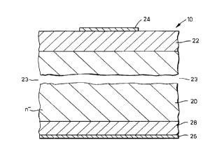
Referring to Figure 1 there is shown an electroluminescent device 10. The device 10
comprises a silicon substrate 20 surmounted by a luminescent porous silicon region
~ 22. Figure 1 is not drawn to scale, as in~lic~ted by discontinuities 23. The device 10
includes a top electrode 24 of l,~nspar~nt indium tin oxide and a bottom electrode 26
of aluminium. The silicon substrate 20 includes a heavily doped region 28 for forming
an ohmic contact with the bottom electrode 26. The porous silicon region 22 has a
mean thickness of 0.4 ~m, the top electrode 24 has a thickness of 0.1 ,~Lm and the
bottom electrode has a thickness of 0.5 ~lm. When a dc electrical current is passed
CA 0221~708 1997-09-17
W 096/29746 PCT/~D5G~ 5
- 12-
between the two electrodes 26 and 24, the device 10 lul l ,i"esces at a peak
waveiength in a range 520-750 nm with a full width at half maximum of between 60and 150 nm.
5 The device 10 is fabricated as follows. In a first step, the heavily doped ohmic
contact region 28 is formed. The formation of a heavily doped region to form an
ohmic contact is a standard silicon integrated circuit process. A back face of a 75
mm diameter wafer of lightly doped n-type, denoted n~, (100) silicon of resistivity in
the range 10 - 20 S2cm is implanted by ion Implantation at an energy of 70 keV in a
10 Varian 350 RD ion beam implanter with a donor~impurity. The donor impurity isphosphorous which is implanted at a dose of 5 x 10'5 cm~2. Following the ion
implantation, the implanted wafer is cleaned by washing the wafer in two chemical
baths. The wafer is immersed in a first bath containing 300 ml of 35% NH3 solution,
300 ml of 30% H2O2 solution and 1500 ml of deionized water at a temperature of
15 88~ C for 15 minutes and then immersed in a second bath containing 300 ml of 35%
HCI solution, 300 ml of 30% H2O2 soluUon and 1500 ml of deiol,i,ed water at a
temperature of 88~ C for 10 minutes. After immersion in the two baths, the wafer is
rinsed in de-ionised water and dried. After cleaning, the i"~plar,led wafer is anr.~~'acl
in argon-2% oxygen at 1050~ C for 30 minutes which results in the formation of a20 thin surface oxide layer on each face of the wafer having a ll ~i~,hr ,ess of approximately 60 A.
In a second step a front face of the silicon wafer is i",planlad with an acceptor
impurity. The acceptor impurity dopant is boron. The boron is i""~la"led in a Varian
25 350 RD ion beam implanter with an ion beam of energy 35 keV and a beam current
of 250 ~A and a beam size of approximately 0.2 x 1.0 mm2. The ion beam is
scanned over the front face of the silicon wafer in a cor,~;~lfY scan pattern which
ensures uniform dosing of the surface. Each scan takes ap,~roxi",dlely 1 second.The wafer receives an implantation having a total i",planldlion time of 10 minutes
30 during which the wafer receives a total dose of 1 x 1016 cm~2. During the
implantation, the wafer is held on a thermal sink which prevents the temperature of
the silicon rising excessively due to the i",plantalion. The temperature of the wafer
rises to no more than 120~ C during the second ion i",planldlion step and it is
estimated that the temperature of the wafer rises to between 30~ and 40~ C .
CA 022l~708 l997-09-l7
W Og6129746 PCT/GB96/OOS89
-13-
ln conventional integrated circuit processing, a silicon wafer would be annealed after
ion implantation to recrystallise and then anneal out any point defects introduced
during the ion implantation and to activate electrically the dopant. Electrical activation
of the boron dopant occurs when the dopant atoms occupy substitutional sites within
the silicon lattice. However, in the present fabrication process, the wafer is not
annealed after ion implantation. This lack of an anneal after the ion implantation
process wouEd be considered undesirable and surprising to those skilled in the field of
silicon integrated circuit processing since the dopant has low electrical activity and
10 the silicon remains in a damaged state.
Measurements of the sheet resistivities of the heavily doped region 28 after annealing
and of the front face after ion implantation have been made. The region 28 had asheet resistivity of 16 Q ~1, which compares with an estimated value for a fully15 activated dopant implant of 10 Q_~~. Therefore within experimental error, the dopant
in the heavily doped region 28 is fully activated. After ion implantation, the front face
had a sheet resistivity of 1800 Q-~~, compared with an estimated value of 10 Q: ~1 if
the dopant had been fully activated. The conductivity of the unannealed implanted
boron layer is less than 1% the expected conductivity if the dopant had been fully
20 electrically activated. Transmission electron microscopy has indicated that the
crystalline slructure of the implanted silicon is heavily damaged by the boron ion
implanlalion.
The ion implanted silicon wafer has been measured using secondary ion mass
25 spectroscopy (SIMS) to determine a distribution of boron within the silicon. Figure 2
shows a plot 100 of dopant concentration in atoms cm~3 against depth from the front
face in mm. The SIMS measurements indicale a peak in dopant concentration 102 of8x 102~ atoms cm~3 a distance of 120 nm below the front surface. Boron has a
maximum solid solubility in silicon of approximately 5 x 10²~ atoms cm~3 at 1200~ C.
30 The peak dopant concentration 102 is thus comparable with the solid solubility limit of
boron in silicon. The implanted silicon has a damaged region which is associatedwith the implanted boron. It is expected that the damaged region has a peak in
damage which is slightly deeper than the peak in dopant concentration 102. Figure 3
shows a schematic representation of a silicon wafer 110 after the second ion
CA 022l~708 l997-09-l7
W 096/29746 PCT/GB96/00589
-14-
implantation process. The wafer 110 has a first region 112 which is heavily doped
with an n-type dopant, denoted n . A second region 114 is doped so as to be a p-type region. A remaining region 116 has the n~ doping of the original wafer. Since
the dopant in the region 114is not fully electricaily active a position for an interface
5 120 between the p-type region 114 and the n region 116 is difficult to determine.
The interface 120 is less than 600 nm from a front surface 122.
Following the second ion implantation step, the porous silicon region 22 is produced
by a light assisted anodization process. Anodization in the context of the production
10 of porous silicon is a generally accepted term for eJectrolytic selective ~isssl~ltion of
silicon. Referring to Figure 4 there is shown in schematic form anodizing equipment
200 for the production of the porous silicon region 22. In the equipment 200, the
silicon wafer 110 is held within an anodizing cell 212. The anodi i"g cell 212 is of
PTFE. The silicon wafer 110 divides the cell into two electrolyte baths 214 and 216.
15 The electrolyte baths 214 and 216 each contain an electrolyte 218 COI~ liaillg a
solution of 40 wt% HF in water (electronic grade). The electrolyte 218 in each bath is
pumped around a respective closed loop (not shown) to provide circulation of theelectrolyte.
20 The anodization process is light-assicted. In order to illuminate a first face 220 of the
wafer 110, the anodizing cell 212 has a polycarbonate window 222 and an 800 W
tungsten-halogen lamp 224 is positioned 24 cm from the face 220 and 14 cm from
the polycarbonate window 222. A water cooled infrared absorb..,g filter 226 is placed
between the lamp 224 and the window 222. The first face 220 cor,~:s,conds to the25 front face of the silicon wafer i",planled with p-type dopant. Measurements of the
light intensity at the window 222 were made using a calibrated silicon photodiode
detector system comprising a Newport model 840-C meter togell,er with an 818-ST
detector. The meter gave a reading of 130 mWcm~2 with a d~lec~or control unit set at
a wavelength compensation of 900 nm.
Each of the baths 214 and 216 contains a respective platinum elect,ude 230 and 232.
The electrode 232 is in the form of a gauze in order to allow the lldnalllission of light
through it. In operation, the electrode 232 is biased negatively, forming a cathode
and the electrode 230 is biased positively to form an anode. A co"sla"l current
CA 0221~708 1997-09-17
W 096/29746 PCT/GB96/00589
source is connected between thè anode and the cathode. In operation an anodizingcurrent with an anodizing current density of 3 mAcm~2 at the silicon wafer face 220 is
passed between the electrodes. The electrolyte is maintained at a temperature ofbetween 16~ and 17~ C. The silicon wafer is anodized for 4 minutes. In the
anodization process a porous silicon region is created which extends through the p-
type region 114 into the n-type region 116.
The anodized silicon wafer is left in the HF containing electrolyte 218 for a further one
minute after l:he anodization is comple~ed and the anodizing current switched off but
still under illumination. The wafer is removed from ,the electrolyte and the wet wafer
is then dried Iby spinning in air at a speed of 2500 rpm for a duration of thirty seconds.
The spinning process is repe~ted six times. Under these fabrication conditions no
evidence of macroporous (pores greater than 50 nm in diameter) silicon has been
observed using scanr,i"J electron microscopy.
The thickness of the porous silicon region after drying has been measured by viewing
a cross section of the silicon wafer in a SEM and also by chemically stripping part of
the porous silicon region from the silicon wafer using a NaOH solution and measuring
a resulting step height between the stripped region and the unstripped region using a
scanni,~g probe height measuring instrument. The thickness of the porous siliconregion 22 was measured to be 0.4 ~m i 0.1 ~m across the wafer. The average
porosity of the porous silicon region was measured using gravimetric techniques to
be 70% ~ 5%
Following creation of the porous silicon region 22 a piece of wafer having a size of
20 mm by 15 mm is cleaved from the centre of the silicon wafer. The top and bottom
electrodes 24 and 26 are then deposited onto this piece of wafer. The top electrode
24 is ~Jeposiled onto the porous silicon region 22 by rf magnetron sputtering using a
a two inch sputter target cor"p,i~i"g a hot pressed and calcined mixture of 90% In2O3
30 and 10% SnO2 available from CERAC Limited. The sputtering was performed at
room le""~el~lure using an rf frequency of 13.56 MHz and a sputtering power of 50
watts in a flowing sputtering gas of 0.09% oxygen in argon at a pressure of 8 x 10⁻³
mbar with the silicon wafer being 6 cm from the target. A film of indium tin oxide
(ITO) is cleposi~ed through a shadow mask to form dots of diameter between 1 and 2
CA 022l~708 l997-09-l7
WO 96/29746 PCT/GB!)G~ x9
- 16-
mm and a thickness of 0.1 llm over a deposition period of 15 minutes during which
the piece of wafer warms to a temperature of approximately 60~ C. It may be
pos~ !e to deposit ITO of the required characteristics in a sputtering gas having an
oxygen content in the range 0.01% to 0.3% with the balance being argon in a
5 pressure range of 2 x 10³ to 1.6 X 10² mbar with a target wafer separation in the
range 1 to 15 cm.
The deposited ITO film has a typical optical transmission coefficient of 85% for light of
wavelength in the range 400-900 nm and has a permeability which is dependent on
10 its thickness. The ITO film has been measured to d,etermine its characteristics using
Hall measurements and has been found to be n-type with an electrical resistivity of
1.6 mQcm. FTIR absorption measurements through the ITO contact show that the
silicon-hydrogen bonds present in the as anodised material are still present after ITO
deposition. In addition there is no evidence for sig,liricant oxidation of the structure
15 during ITO deposition. The ITO layer may be permeable depending on its thickness.
Chemography measurements of sarn~ es with a 0.1 ~Lm thick ITO layer have
c~led that the ITO is per",~e e whereas samples with a 0.2 ~Lm thick layer
showed s4"i~icar,lly less permeability. This technique is described by L.T.Canham et
al. in Advanced Materials Volume 6 Number 11 1994 pages 865-868. In the
20 chemography measurements a piece of unexposed pholoyl~phic film is placed in
contact with the sample in the dark for a period of time and then developed. When
porous silicon is placed in contact with the photographic film silane produced by a
reaction between the porous silicon and moisture in the air reacts with the
photosensitive chemicals on the pholoy,~phic film so that after development a dark
25 "image" is formed. The production of an image with the ITO covered samples
indicates that the ITO is permeable and at least silane is passi"g through the ITO
probably together with water vapour in the opposile direction.
The bottom electrode 26 is deposited onto the bottom of the piece of wafer using a
30 ll ,e",)al evapor~lion process. The aluminium is evaporated in a vacuum of
approki",dl~:ly 10-6 mbar to a ll~icl~r~ess of 0.5 ~Lm. In conventional integrated circuit
manufacture an evaporated ohmic contact would be annealed in forming gas a
mixture of nitrogen and hydrogen at 425~450~ C. This annealing procedure is not
carried out in the creation of an ohmic contact to the device 10. The deposition of a
CA 0221~708 1997-09-17
W O 96/29746 PCTIGB96100589
bottom electrode is not a critical step in the manufacture of a porous silicon
electroluminescent device. A device may be made to luminesce with direct electrical
contact to the heavily doped region 28.
- 5 In order to obtain luminescence from the device 10, electrical contact is made to the
top and bottom electrodes 24 and 26. Referring to Figure 5 there is shown a device
10 to which electrical contact has been made to the top and bottom electrodes 2aand 26. Electrical contact to the bottom electrode 26 is made by a metal crocodile
clip 300 to which a wire 302 has been attached. A piece of mica 310 is placed
between the clip 300 and the porous silicon region, 22 to protect the porous silicon
and to provide eiectrical insulation between the clip 300 and the porous silicon region
22. Electrical contact to the top electrode 24 is made by a sprung gold wire probe
312 of diameter 30 mm. The wire 302 and the probe 312 are connected to a
computer controlled power supply (not shown).
Referring to l=igure 6a there is shown equipment 400 for the measurement of light
output from the device 10 as a function of current through the device and applied
voltage. Measurements of light output are generally made at room temperature butmeasurements can also be made at elevated and reduced temperatures. The device
10 is placed inside a vacuum chamber 410 having a glass window 412. Electrical
contact to the probe 312 and the wire 302 is made through a feedthrough 414. Thechamber 41~ is evacuated through a port 416 connected to a rotary pump (not
shown) to an approximate pressure of 0.05 mbar as measured by a calibrated
capacitance manometer. An imaging system 420 comprising a microscope 422 to
which a CCD camera 424 and a photomultiplier 426 is connected is used to observethe emission of light from the device 10. The photomultiplier 426 may be replaced by
an optical multichannel analyser (not shown). A beam splitter 428 in the microscope
422 splits received light between the camera 424 and the photomultiplier 426. A
beam of blue light of wavelength 442 nm from a laser 430 may be directed onto the
device 10 for photoluminescence measurements. During photoluminescence
measuremenl:s, a cut-off filter 432 is inserted into the microscope 422 in order to filter
out blue light From the laser 430.
CA 0221~708 1997-09-17
W 096/29746 PCT/GB96/00589
In order to obtain measurements of the output efficiency of the device 10 the imaging
system 420 is replaced by a detection system 440 as shown in Figure 6b. The
deteclion system 440 comprises an optical fibre 450 which receives light from the
device 10 and guides it to a spectrometer 452. An input face 454 of the optical fibre
5 450 is positioned at a distance x from the device 10 and at a normal incidence to the
centre of the device.
The combination of the optical fibre 450 and the spectrometer 452 was calil,,~led for
sensitivity as a function of wavelength using an ar,~,1gel"e"1 shown in Figure 6c.
10 The input face 454 is positioned at a distance d appro~illlaLely three metres from a
calibrated tungsten light source 456 and a spectrum 458 is recorded. The
spectrometer 452 includes a diode array detector of a multichannel type in whicheach separate channel corresponds to a given wavelength range from ~n ~ ~J2 to
~n + ~?~/2. For example a channel 460 corresponds to a range 620 to 620.6 nm. The
15 central wavelength ~n~ of channel n is determined by measuring the channel number
of the peak of a series of known spectral features such as laser lines. The recorded
spectrum 458 is a measure of intensity as a function of wavelengll " /N (n ?~n ) where
/N (n ~n ) denotes the number of counts per second in channel n covering the
wavelength range from ?~n - ~?J2 to ?~n + ~?./2. The su,uer~ ut N denot~s that the
20 measured signal is in counts per second.
The light output from the light source 456 was previously calibr~Led to obtain ameasure of the output as a function of wavelength L (?~), in units of watts m~2 nm~1 for
a distance of 0.5 m from the source. The output at a di;~lance d Ld (;~J is obtained by
25 multiplying L (?~) by (0.5/d)2 where d is in metres.
The measured signal in channel n corresponds to a power density at the input face
454 of Ld(?~ ?~ having units of watts m~2. The power sensitivity of channel n,
sP (n,~n ), iS given by
SP (n, ?~n ) = ( Ld (?~n ) . ~?.) // N (n ~n )I
where ~?~ is the spectral width of each channel of the detector in nm. SP (n,?~n ) is in
units of watts m~2 / (counts per second).
CA 022l~708 l997-09-l7
W 096/29746 PCT/~5''~0589
-19-
The sensitivity of channei n of the detection system 440 in terms of pho~on flu,~
density, sQ (n~ is given by
S (n, ~n J = ( L (n, ~n ) . ,~. / Epi n ) / I N (n i
where Epin is the energy of a photon of wavelength ;~n and is given by
Ep~ n = h . c / ~n.
where h is Planck's constant and c is the velocity of light. The units of sQ (n.in) are
photons sec~~m~2/ (counts per second).
From measurements of the light output by the device 10 at a distance x an intensity
15 spectrum, /ND (n,ln ). is obtained in counts per second. The number of photons output
at position x per m2 per secondQx, is given by
Qx = ~ I D (~ n J sQ (n~n )~
20 where the summation is over n, the number of channels of the detector.
The dependence of the output of the device 10 as a function of angle has been
measured up to angles of + 45~. It was found that in this angular range, the intensity
of the output was Lambertian, i.e. proportional to Cos (~), where ~ is the angle to the
25 device normal. It is assumed that the output is also Lambertian for the angles
45O<~<90~ .
The total number of photons output per second from a Lambertian source. Qtor,is
given by
Qtot= Qx-~-X2.
. CA 022l~708 l997-09-l7
W 096/29746 PCT/GB~ YQ~
-20-
The output external quantum efficiency, EQE, in per cent (epr~senting the
percentage of photons emitted from the device per electron injected is given by
EQE = (100 . Qtot ) q /1,
where q is the charge per electron and the current through the device, I, is in amps.
Referring to Figure 7 there are shown results of electrolumil,escence measurements
and photoluminescence measurements which have both been corrected for
10 instrumentai response. A graph 500 shows outpu~ light inl~nsily, in arbil,dry units
against wavelength. The results of the photoluminescence measurements, obtained
by illuminating the device 10 with blue light from the laser 430, are shown by a line
510. A photoluminescence peak in output i"Lensily 512 was observed at a
wavelength of approximately 610 nm. Typically, photoluminescence output intensity
15 peaks are measured to be in a range 600-750 nm. When viewed by eye under
ultraviolet light, the porous silicon region exhibits orange phot~ i,-escence.
The results of the electroluminescence measurements, obtained by passi..g a dc
electrical current through the device 10, are shown by a line 520. An
electroluminescence peak in output intensity 522 was observed at a wavelength of590 nm. The photoluminescence peak 512 thus occurs at a longer wavelehglh than
the electroluminescence peak 522. Typically, electroluminescence output intensity
peaks are measured to be in a range 520-750 nm with a full width half maximum
spectral width in a range from 60 nm to 150 nm.
Electrical measurements of the device 10 have shown it to be rectifying and that it is
forwards biasable by the application of a positive voltage to the top elec~,ode 24.
This polarity dependence is the same as that which would be ol,ldi"ed from a device
with a p-n junction within it, such that the p region of the p-n junction is on the porous
30 silicon side of the wafer. Referring to Figure 8 there is shown a log-linear plot 550 of
the electrical measurements of the device 10, showing the current through the device
as a function of applied voltage. In Figure 8, the current-voltage cl.a.d~ i ;lics of the
device 10 are plotted as the current density in Acm~2 against the applied voltage in
volts. A positive applied voltage corresponds to a positive bias to the top elE.,llode
CA 0221~708 1997-09-17
W 096/29746 PCT/~D~CI~~9
24. Figure 9 shows in greater detail the current-voltage characteristics of the devic_
10 when the device is positively biased. Figures 8 and 9 collectively demonstrate
that the device 10 is rectifying with the same polarity dependence as a p-n junction.
5 A p-n junction diode may be characterized by an ideality factor, n, where
n - (q/kTJ . (~V/~(ln J)),
where J is the current density and V is the potential difference across the diode. In
10 an ideal case, a p-n junction diode has an ideality factor of unity. For the device 10 at
values of applied bias less than 0.5 V, the diode ideality factor of the device is 2. For
forward biases greater than 2 V, voltage dependent ideality factors greater than 10
have been measured.
1~ Electroluminescence from the device 10 has been detected using the measuring
equipment 400 at an applied current density of 0.01 Am~2, which from Figure 9
corresponds to an applied voltage of approximately 2.6 volts. A threshold current
density above which the device 10 luminesces might be less than this figure since the
minimum measured current might be limited by the optical detection limit of the
20 measuring equipment 400. Electroluminescence from the device 10 is visible to the
unaided human eye at an applied current density above an applied current densitythreshold of 0.1 Am~2. With more sensitive detection equipment, luminescence at an
applied current density of 0.0001 Am~2 has been detected with a corresponding
threshold voltage of 1.7 V.
Referring to Figure 10 there is shown a plot 600 of light output power in microwatts as
a function of applied current density in Acm~2 for a device similar to the devlce 10.
having an area of 0.01 cm2. Lines 610 and 612 are lines of constant external
quantum effciency. Any line parallel to the lines 610 and 612 is also a line of
30 constant efficiency. The line 610 corresponds to an external quantum emciency of
0.01% and the line 612 corresponds to an external quantum efficiency of 0.1%.
Figure 11 shows a plot 660 of external quantum effciency against current density for
a device similar to the device 10. The plot 660 shows that the device had an output
CA 022l~708 l997-09-l7
W 096/29746 PCT/GB96/OOS89
-22-
quantum efficiency greater than 0.01% above an applied current density of
0.01 Am~2. The measured device had an external quantum efficiency of greater than
0.1% at an appiied current density in a range between 0.2 Am~2 and 7.0 Am~2. Thedevice has a maximum room-temperature external quantum efficiency of 0.18% at an5 applied current density of 1.0 Am~2.
The above efficiency results were obtained for a device operating in a vacuum at a
pressure of 0.05 mbar. Referring now to Figure 12 there are shown measurements
of the output efficiency of a device at two different vacuum pressures as a function of
10 time. A line 700 is a plot of measurements carriedput in pressure of 0.05 mbar. At
0.05 mbar the output efficiency falls by a factor of four over a period of five hours. A
line 710 is a plot of measurements carried out at a pressure of 7.3 mbar. At 7.3mbar. the efficiency falls by a factor of 100 in a few minutes. The observed
degradation in output efficiency is accompanied by an increase in the voltage
required to maintain a constant current. Degradation is reduced if the device isoperated in dry nitrogen compared with operation in wet air. Since the ITO contact to
the device is permeable the active region of the device may interact with the
surrounding environment. It is therefore concluded that the quantum er~i~;en~;y of the
device 10 is degraded by exposure to water or oxygen. The co" ldlion of the
device 10 and the vacuum chamber 410 form an enc~rsu'~ted electroluminescent
light emitting device.
For electroluminescent devices having the ITO replaced by a gold top electrode the
gold must be thin to be se",ill~nsparent. However chemography measurements
have shown that a gold thickness of greater than 1000 A is required to stop ingress of
moisture leading to degradation of the device. This thick~,ess of gold is too great for
obtaining efficient luminescence through the top contact.
Electroluminescent devices having ITO top electrodes which are thicker than 0.1 ~Lm
30 exhibit luminescence characteristics which differ only slightly hetwccn oper~lion in air
and operation in vacuum. Figure 13 shows the change in efficiency with time for a
device similar to the device 10 except that the top ITO electrode is 0.2 ~m thick and
correspondingly iess permeable than the top electrode 24. A line 720 shows the
change in efficiency with time for the device operating in vacuum and a line 725
CA 0221~708 1997-09-17
W 096/29746 PCTr~D,./~ ~Q9
shows the change for the device operating in air. Figure 13 shows that, contrasting
with Figure 12, the degradation of a device with a thicker ITO top electrode operating
in air is not significantly different from that of a similar device operating in vacuum. It
should be noted that the current density applied to the device to obtain the results
5 shown in Figure 13 was much higher than that to obtain the results shown in Figure
12, and hence the degradation was much more rapid.
Measurements of the external quantum efficiency of the electroluminescent devices
as a function of temperature have shown a maximum external quantum efficiency of10 0.4% at a temperature of 200 K (-73~ C).
Referring to Figure 14 there is shown a graph 7~0 of output power as a function of
time for a device similar to the device 10 across which a dc bias voltage modulated
by a 10 kHz square wave. Figure 14 shows modulation of the light output of a device
15 in response to a modulation of the applied voltage. Figure 15 is a plot of the results
of modulated output measurements at modulation frequencies of up to 1 MHz.
Figure 15 shows that a modulated output can be detected at frequencies of up to 1
MHz.
20 In order to determine how the boron dopant is distributed in the device 10, SIMS has
been used to measure the distribution of boron through the porous silicon region 22.
Figure 16 shows a plot 800 of boron concentration against depth for a silicon wafer
after the first and second ion implanldlions and after the anodization and drying
stages but before deposition of the top and bottom electrodes. The plot 800 shows a
25 peak in conc:entration 810 close to the surface of the porous silicon and a plateau
region 812 in which the boron concer,lldLion is effectively constant. The approximate
position of the interface between the porous silicon and the bulk silicon is indicated by
a chain line 814. Figure 16 also shows a plot 820 of fluorine concentration and a plot
822 showing the measured silicon secondary ion counts.
As a comparison to Figure 16, Figure 17 shows a plot 850 of boron concentration as
a function of depth for a silicon wafer after a five minute anodization which was
annealed between the second ion impiantation and the anodization. This anneal
comprised the steps of heating the wafer in nitrogen at 525~ C for 6û minutes then
CA 022l~708 l997-09-l7
W 096/29746 PCTIGB96/0058
-24-
heating the wafer in oxygen at 950~ C for 60 minutes followed by a dip in buffered HF
to remove any oxide layer. The plot 850 shows a peak in concentration 860, similar
to the plot 800. but there is no plateau region equivalent to the plateau region 812.
The plot 850 shows a similar boron concentration profile as that shown by a SIMS5 measurement carried out on a wafer after the anneal but before ano.li~dlion. Figure
15 also shows a plot 862 of the silicon secondary ion counts. Although samples
which were annealed after the second ion i~planlalion did exhibit
electroluminescence, the efficiency of this electroluminescence was lower than that
for unannealed samples.
From a comparison of Figures 16 and 17, having regard to the disappeardnce of the
plateau region 812, it is concluded that transportation of the boron dopant is more
significant during the anodization process if the wafer is not annealed after the boron
implantation prior to the anodization. The boron might be transported via the liquid
15 anodization electrolyte or within the silicon itself.
If transportation of boron takes place during the ano~ lion p,ucess, the following
mechanism for the creation of a p-n junction within the porous silicon is envisaged.
Once pores have been created in the p-type region 114, the porosity e,cler,ds into the
20 region 116. As formed, porous silicon in the region 116 is n-type in nature. As the
anodization progresses and the depth of the porous silicon region increases, the n-
type porous silicon is doped by boron transported from the p-type region 114 so that
it becomes p-type porous silicon. In consequence, near to the advancing interface
between bulk silicon and porous silicon, it is considered that there is a newly formed
2~ n-type porous silicon region and further towards the surface of the wafer the porous
silicon is doped p-type by the transported boron. This would produce a p-n junction
in the porous silicon region. When the anodi~lion process is ter",il,~led, a region of
n-type porous silicon would remain close to the bulk silicon - porous silicon interface
and so the p-n junction in the porous silicon region would remain after the ano.li~dlion
30 process has finished. Luminescent porous silicon is only created when the
anodization front extends into the region 116. Thus it is believed that a p-n junction is
created within a region of luminescent porous silicon.
CA 022l~708 l997-09-l7
W O 96/29746 PCT/GB96/00589
-25-
ln order to investigate the formation mechanism for the p-n junction in the porous
silicon region, experiments have been carried out to investigate the effect of changing
the anodization time. Samples were anodized for different times. t. and after
anodization, the samples were left in the anodizing electrolyte, with the illumination
5 left on, for 5-t minutes after anodization to ensure that once a porous silicon region is
formed it receives the same leaching effect as it does when a wafer is anodized for
five minutes. In the production of the device 10, the preferred anodization time is four
minutes follovved by a one minute leach. After fabrication, photoiuminescence and
electroluminescence measurements were carried out on devices fabricated from the10 anodized silicon. These measurements are summarjized in Table 1.
The following conclusions may be reached from the information provided by Table 1.
Table 1 shows that a device fabricated from the anodized wafer becomes strongly
rectifying after anodization for more than two minutes. This suggests that the feature
15 of the device 10 responsible for the rectifying behaviour, a p-n junction, is at a depth
at least equal to that corresponding to the depth of porous silicon formed after two
minutes of anodization, or approximately 0.15 ,um. There is also a marked change in
the values Gf the electrical power required for detectable electroluminescence
between two and three minutes anodization.
Table 1
Anodization IV Curve Electrical Power for Maximum Electro-
time/minutes Rectifying? Detectable Electro- luminescence
luminescence /llW External Quantum
Efficiency
1 Weakly 54 6 x 10⁻⁵ %
2 Weakly 37 3 x 10⁻³ %
3 Strongly 0.02 0.15 %
4 Strongly 0.02 0.18 %
Strongly 0.02 0.13 %
CA 0221~708 1997-09-17
W 096/29746 PCT/~'iG10~X9
Electroiuminescent devices have been fabricated from silicon wafers which had been
subject to a boron ion-implantation different from that for the device 10. The wafer for
the device 10 received a boron dose of 1 x 10l6 cm~2. Devices made from a wafer
which received a dose of 3 x 1 o16 cm~2 had an approximate maximum external
5 quantum efficiency of 0.026%. Devices made from a wafer which received a dose of
3 x 101~ cm~2 had an approximate maximum external quantum efficiency of 0.062%.
The devices made from wafers which had received boron doses which were greater
than or less than the dose for fabricating the device 10 thus had siyuificalllly lower
efficiencies. However since there are a large number of processi"g conditions which
10 may be altered individually changing other processing conditions in combination with
a change in the boron dose may result in devices of even higher efficiency.
When ion implantation of the boron is carried out at a beam current of 25 ~A rather
than the standard 250 ~LA with the same total dose both ele~l,oluminescence and
15 photoluminescence from a device have a deep red appearance to the eye rather than
the usual red-orange appearance. Also a device fabricated accor-Ji"g to the
preferred procedure which initially displayed electroluminescence which had a red-
orange appearance to the eye displayed electroluminescence which was green-
yellow in appearance after being stored in air for a week. These observations
20 indicate the possibility of tuning the fabrication process to produce electroluminescent
devices suitable for colour dispiays. Since the device 10 is fabric~led from a wafer of
siiicon it would be a relatively straight forward procedure to integrate the device 10
with other non-luminescent silicon devices such as transistors on a single piece of
silicon to form an opto-electronic integrated circuit. Since the silicon is not annealed
25 after the acceptor impurity ion implantation it would be feasible to l~briodle these
other silicon devices prior to the fabrication of the electrolu",inescenl device 10 with
regions of the silicon wafer containing the non-luminescent devices being masked off
by for example silicon nitride deposited by a low temperature plasma enhanced
chemical vapour deposition process.
Materials other than ITO have been used for the top electrode. Gold indium and
aluminlum have been used and whilst devices incorporating top ele~ udes of thesematerials do exhibit electroluminescence the efficiencies are red-lced The bottom
electrode 26 is not critical to the operation of the device 10. Electroluminescent
CA 0221~708 1997-09-17
W 096/29746 PCT/GB~ 05~9
-27-
devices in which the bottom electrode is absent have been operated with little
difference in the device d.c. electrical characteristics from those of the devlce 10.
though it is likely that the high frequency behaviour would be significantly different.
5 Electroluminescent devices have also been fabricated by anodizing a wafer of nsilicon to form a porous silicon region and then immersing the porous silicon in a
solution of boric acid. SIMS measurements confirmed that boron had been
introduced into the porous silicon at high concentrations but electroluminescence
efficiencies from devices made by this method were low, having external quantum
10 efficiencies oF the order 0.002 %.
From the sheet resistivity measurements, it is estimated that less than 1% of the
implanted boron is electrically active in the region 114 after ion implantation. The
electrical measurements of the device 10 show p-n junction diode behaviour. It can
15 therefore be concluded that the boron dopant is electrically active after theanodization process. Since there is no annealing carried out after the boron ionimplantation, it is possible that the electrical activity of the boron dopant after the
anodization process is due to surface doping of quantum wires in the porous silicon
by transported boron. The term surface doping refers to the deposition of dopantspecies on the surface of the quantum wires. Since the quantum wires are less than
30 A in width, these dopant species may remain on the surface and modify the band
structure of the silicon or they may diffuse the short distance into the quantum wires.
The surface doping scenario is supported by the experiments involving immersion of
25 n- porous silicon in boric acid. Referring to Figure 18 there is shown in schematic
form a possible ",icroscopic structure of the device 10. It is emphasised that Figure
18 is only schematic and is not to scale. Figure 18 shows four quantum wires 900joined to a silicon substrate 910 at one end and surmounted by a layer of ITO 920 at
an opposite end. Each of the quantum wires 900 has a top region 930 which is a
30 remnant of the second region 114 of Figure 3. During the anodization process, it is
believed that boron dopant is transported with the advancing interface between the
porous silicon and the bulk silicon. Some of this boron dopant is deposited onto the
surface of the quantum wires as a layer 940. A region 950, together with a region
930, of each silicon quantum wire 900 which is in close proximity to the layer 940 has
CA 0221~708 1997-09-17
W O 96/29746 PCT/GB96/00~89
p type electrical characteristics as a result of surface doping effects of the layer 940.
A region 960 of each quantum wire 900 which does not have a surface layer of boron
dopant remains n-type. An interface between the n-type regions of the quantum
wires and the p-type regions of the quantum wires is indicated by a dashed line 970.
Transmission electron microscopy of the porous silicon region 22 after ion-milling has
identified that the porous silicon comprises quantum wires of width less than 3 nm
and surprisingiy small pores having a diameter of ap~roxil,lately 7 A. Pore widths in
a range from 15 A to 30 A have been observed previously. It is possible that the10 exceedingly fine porosity could play an important,role in the pe~runllance of the
device. As discussed by Canham and Groszek in Journal of Applied Physics,
Volume 72, Number 4, 1992, pp 1558-1565, microporous silicon has pores of size
less than 20 A wide. Microporous silicon has been subdivided into supermicroporous
silicon with a pore size of approximately 10-20 A wide and ulLIdrlli~ ,porous silicon
15 with a pore size of less than approximately 10 A wide. The pores in the freshly
etched device structure are probably supermicroporous, becoming ullldrl~icr~po-uus
upon skeleton oxidation.
It is known to be diffficult to dry porous silicon structures which have a pore size less
20 than 20 A. SIMS measurements indicate a high level of fluorine in the porous silicon.
It is therefore possible that HF trapped in the pores could protect the internal surface
of the porous silicon against oxidation prior to device operation.
SIMS data indicates that a surface region of the porous silicon region 22 has
25 significant levels of oxygen, carbon and fluorine in addition to boron. It is therefore
possible that the surface region, although not strongly luminescent, has a co~ dldble
or wider band gap to an active luminescent region below it. It would lher~rurt: act as
an efficient hole injection layer for the device 10. Hole ill;e ';Qn efficiency may be
quantified by a minority carrier injection ratio, g, defined as the ratio of the minority
30 carrier current to the total current passi"g across the relevant junction, as desc,iLed
by S.M.Sze in "Physics of Semiconductor Devices", ~lley and Sons, New York,
1981, page 268. An efficient hole injection layer might have a minority carrier
injection ration, g, of more than 10-3 at bias voltages below 5 volts. It is thought that
CA 022l~708 l997-09-l7
WO 96/29746 PCT/~b~ v05
- 29 -
an external quantum efficiency of 0.1% corresponds to an internal quantum efficiency
of approximately 1%, which implies a value of g of at least 1 o-2.
Referring now to Figure 19. there is shown a hypothetical band structure 1000 of the
~ ~ device 10 in an unbiased state obtained using a device simulation program. In the
device simulation, the following parameters were used:
(a)- a pOI-OUS silicon band gap of 2 eV derived from the peak of the
photoluminescence spectrum;
10 (b)- an electron affinity of 3.86 eV, from T. Var,l Buuren et al., Applied Physics
Letters, Volume 63, page 291 1, 1993;
(c) - donor and acceptor binding energies of 0.35 and 0.65 eV respectively, from T.
Van Buuren et al. as above and C. Delerue et al., This Solid Films. Volume
255, page 27, 1995;
15 (d)- dielectric constant of 3.8 for 75% void and 25% silicon, from D.A.G.
Bruggeman, Ann. Phys., Volume 24, page 636, 1995; and
(e) - an active boron concentration profile deduced from SIMS measurements and
multiplied by 0.01% to allow for most of the boron dopant not being electricallyactive.
A line 1002 represents the conduction band, a line 1004 represents the valence band
and a line 1006 represents the Fermi level. The n-type bulk silicon has a band gap of
1.15 eV, as indicated by a region 1010 of the band structure 1000. The n-type
porous silicon band structure is indicated by a region 1012 and the p-type porous
25 silicon region band structure is indicated by a region 1014. The ITO is n-type with a
band gap of 3.7 eV, as shown by a region 1016. The simulation predicts a p-n
junction in the porous silicon at a depth of 400 nm from the ITO/porous silicon
interface.
30 Figure 20 shows the hypothetical band structure after the application of a positive
bias to the 110 relative to the bulk n-type silicon. Most of the applied potential is
dropped across the p-type porous silicon. The conduction band of the ITO thus
moves down relative to the valence band in the p-type porous silicon. Electrons 1020
in the valence band of the p-type porous silicon can then tunnel into unoccupied
CA 0221~708 1997-09-17
W 096/29746 PCT/GB~C;~X9
-30-
states in the conduction band of the ITO which is equivalent to injecting holes 1022
into the valence band of the p-type porous silicon. Electrons 1026 from the
conduction band of the n-type bulk silicon are transported across a barrier 1028retween the n-type bulk silicon and the n-type porous silicon into the conduction
band of the n-type porous silicon. The holes in the p-type porous silicon and the
electrons in the n-type porous silicon are transported towards the interface region
between the p-type and the n-type porous silicon. Within this region the electrons
and holes may recombine. This recombination may either be radiative or non-
radiative. An estimated 90% of photons generated by radiative reco",bination are10 absorbed within the device 10. The remainder are, emitted and result in the visible
electroluminescence.