Note: Descriptions are shown in the official language in which they were submitted.
CA 02216367 1997-09-24
W O 9613;6114 PCT/GB~6/00405
sIDIR~cTIoNAL TR~MTSSION LIN~ DRIV~R/~ v~K
CROSS~ ~K~N~ TO R~T~TFn APPLICATION
Thi_ a~plication i5 a continuation-in-~art of co-pending application
serial number 08/376,708 filed January 23, 1995, for a Bidirectional
Transmission Line Driver/Receiver.
RArR~.ROuND OF THE lNV~NllON
Field of the invention
A tr~n~;ssion line transceiver is disclosed. More particularly, a
tr~n ;ssion line transceiver having an active transmission line
terminator and variable level signal source is disclosed which is well
adapted for simultaneous bidirectional operation.
Descri~tion of Related Art
AS the operating speed of computer processors continues to increase,
additional d -n~c are placed on devices that must send and receive logic
signals.
In measuring high frequency signals, the measurement sample rates
are, o~ course, higher than in measuring lower frequency signals.
Measuring the precise magnitude of a signal at high sample rates is more
difficult than at lower rates because transient conditions, which may not
have any appreciable effect within the relatively long time period of a
lower frequency samPle rate, may have a significant effect in the shorter
~eriod of a high frequency sample rate.
one high frequency effect of particular concern in the present
invention is that of signal reflection, which occurs when the impedance of
a ;cation path does not match the im~edance of a terminating load on
the receiving end of the path. (The ;cation ~ath between a sending
and a receiving device includes a path such as a bus between devices on a
single circuit board or a cable between devices on different boards. In
any case, because the present invention cnncernC relatively high fre~uency
signals which require a consideration of transmission line effects, the
, ;cation path may be referred to herein as a transmission line.)
Ideally, a terminating load will sink a transmitted signal immediately
u~on the signal arriving at the load so that the magnitude of the signal
may be sampled ;mmP~i~tely upon its arrival at the load and a precise
value of the signal magnitude may be detPrminPd from the sample. However,
if the te ;n~ting load does not match the transmission line impedance,
CA 02216367 1997-09-24
W 096/36114 PCT/GB96/00405
then the load will sink only a portion of the signal upon the signal~s
initial arrival. The rPm~in;nq portion of the signal will be reflected
back onto the transmission line. Ty~ically, depPn~;n~ u~on a number of
factors, at least a part of this reflected portion of the signal will
ultimately be reflected from other loads on the transmission line back to
the terminating load, and this reflection back and forth among loads on
the line will repeat, until eventually more and more of the signal will
sink through the terminating load.
The effect of this signal reflection is, at best, to delay the time
at which the signal may be accurately sampled until such time as the
signal has gone through perhaps many cycles of reflection on the
transmission line. At worst, in the case where a significant part of the
reflected portion is dissipated in the transmission line itself, or sinks
in other loads on the transmission line, the effect of this re~lection is
to greatly reduce the precision with which the magnitude of the signal can
be measured, perhaps to the point where the logic value of a signal cannot
be accurately determ;ned at all. Therefore, it is advantageous to
eliminate, or at least greatly reduce, signal reflection by matching,
insofar as possible, the im~edance of a term;n~ting load and that of a
transmission line.
It is well known to send multivalued logic signals from a sending
device to a receiving device in order to facilitate simultaneous
bidirectional transmission. For a multi-valued logic signal, a receiver
must be more discriminating than a receiver that merely detects an on
condition and an off condition. That is, a receiver for multi-value logic
signals must measure the magnitude of a received signal with a relatively
higher degree of precision than a receiver that must merely detect the
presence or absence of a signal. Thus, there is even greater incentive
for impedance matching for high fre~uency signals which are multi-valued.
While it is relatively straightforward and ecnnom;cal to manufacture
a transmission line between devices with tight control of the line
tm~e~Ance~ it is not as simple to ecnn~ ;c~lly manufacture a fixed
tPrm~nAting load within tight impedance limits. Therefore, it is
desirable to be able to actively adjust termination ;~redAn~e and logic
signal current during operation to eliminate or greatly reduce signal
reflection using Pnts which may be manufactured ecnnnm;cally.
T -~Anre matching using active devices could be achieved by
providing, in addition to the transmission signal, a first signal over a
first reference line from a sender to a receiver informing the receiver of
the amplitude for a logic signal, and a second signal over a second
reference line from a receiver to a sender informing the sender of the
CA 022l6367 l997-09-24
AT9 -94-223 New~Pag~: 16 April ~997;
. ~ ~ ,. . .. .
impedance of a transmission line terminator in the receiver. However,
parti_ularly where a number of senders and receivers are interconnected on
the transmission line, this arrangement is disadvantageous because of the
number of reference lines required. Therefore, it is also desirable to
minimize signal reflection with a single reference line between devices on
the transmission line.
An adaptive circuit which adjusts the output impedance of a reference
driver to that of a reference transmission line and generates a control
voltage for adjusting the output impedances of other drivers on the same
chip to the same impedance is described by Patel et al in "An adaptive
CMOS transmission line driver", Proceedings: Sixth Annual IEEE
international ASIC Conference and Exhibit, Rochester, NY, USA, pages 460-
~63. Impedance mismatch is apparently significantly reduced.
US-A-4620188 describes a multi-level logic circuit including at least one
input level detector which can receive one or more multi-level inputs, a
control switching device, and an output level generator delivering a
single multi-level output. The generalised circuit enables derivation of
various logic gates operating in any chosen base n.
SUMMARY OF ~HE INVENTION
In a first aspect of the present invention, there is provided a
sending device (driver) and a receiving device interconnected by a
transmission line with a certain characteristic impedance for
~nmmllnlcating logic signals over the transmission line between the
devices. The driver has a source for sending the logic signals, and a
reference generator connected to the source for setting the magnitude of
the signals sent by the source. The receiver has a transmission line
terminator for sinking the signals, and a re~erence generator connected to
the terminator for setting a bias of the terminator to establish a certain
family of terminator impedances for sinking the signals. The driver
reference generator and the receiver reference generator interactively
match the terminator im~edance to the transmission line for the set
magnitude of the signals.
It is preferred that the sending and receiving device circuitry for
generating and receiving digital signals over a transmission line is
responsive to externally generated digital data input and control signals.
A reference circuit providing a first and second reference signal is
preferably common to the signal generating and receiving circuitry. In
particular, it is preferred for a single reference line to be used for
transmitting reference sig~als between the sending and receiving devices.
~ .GN~ t~~~
CA 02216367 1997-09-24
AT9-94-223 ~ew Page. ih ApFil 1~97
,, ~
3a
According to a preferred embodiment of the invention, the signal
generating circuitry includes a signal source c~nnected to the
transmission line for generating a variable level digital signal, and a
reference level adjusting and switching circuit ("RLA/S circuit~l) which is
responsive to the digital data input and the first reference slgnal. The
RL~/S circuit is connected to the signal source for selecting the level of
the variable level digital signal and providing a switching signal. The
signal source output is thus adjusted and switched so that the signal
source generates a digital signal to the transmission line which follows
the digital data input at the selected output signal level.
It is also preferred that the signal receiving circuitry includes a
variable input impedance circuit connected to the transmission line which
is responsive to the second reference signal for receiving variable level
;s~ E~
CA 02216367 1997-09-24
W 096/36114 PCT/GB96/00405
digital signals from the transmission line. It also includes a detecting
circuit connected to receive the variable level digital signals from the
variable input impedance circuit. The detecting circuit is responsive to
the first reference signal and detects logic states of the variable level
digital signals as determ;nPd by the first reference signal. The
detecting circuit also converts the detected logic states into
corresponding logic signals of predeterm;ned output levels.
In further aspects of the signal generating circuitry, the RLA/S
circuit speeds up switching of the signal source while maintAin;ng the
signal source digital output signal at a level not ~Xcee~in~ that set by
the first reference signal. That is, in generating the digital out~ut
signal the signal source switches between a first and second Out~ut state,
the switching speed of the signal source being dependent upon the level of
the switching signal applied to the signal source, and during an initial
switching stage a level of the switching signal provided to the signal
source by the RhA/S circuit is boosted to a level greater than that set by
the first reference signal so that the switching circuit increases the
switching s~eed of the signal source. Then, following the initial
switching stage, the level of the switching signal conforms to the first
reference signal so that the signal source digital output signal does not
exceed the level set by the first reference signal.
In still further aspects of the signal generating circuitry, an
Out~l1t level override circuit is included. The override circuit is
connected to the RLA/S circuit, and, in response to the digital control
signal, overrides the selected output signal level set by the first
reference adjustment signal so that the output signal is instead set at a
certain ~redeterm;ned ~ X;~llm level.
In further aspects of the invention, the common reference circuit
al80 provides a third reference signal, and the signal receiving circuitry
further includes a fixed input impedance circuit connected to the
transmission line for receiving the variable level digital signals from
the transmission line. In connection with the fixed impedance circuitry,
a second detecting circuit is connected to receive the variable level
digital signals from the transmission line. The second detecting circuit
is responsive to the first and third reference signals, and detects logic
states of the variable level digital signals as determ;ned by the first
and third reference signals. The second detecting circuit also con~eLLs
the detected logic states into corres~nn~;n~ logic signals of
predet~rm~ne~ output levels.
In -qtill further aspects of the receiving circuitry, in response to
one of the Pxtern~Al control signals the variable input ;~re~Ance circuit
CA 02216367 1997-09-24
W 096/36114 PCT/GB96/00405
assumes a disabled mode having a high input impedance so that the
transmission line is unloaded.
Still other objects and advantages of the present invention will
become readily apparent to those skilled in this art from the following
detailed description. The ~referred embodiment of the invention is shown
by way of illustration of the best mode contemPlated for carrying out the
invention. Other e~bodiments are possible and the details may be modified
in various respects without departing from the invention. For exam~le,
voltages could be used for logic signals instead of currents. As another
example, a field effect transistor ("FET") is selected as a tPrm;n~tor for
the transmission line. Bipolar devices could also be ~elected. Also,
while a shielded reference line and transmission line are shown, non-
shielded lines may also be suitable. Accordingly, the drawing and
descri~tion are to be regarded as illustrative in nature, and not
rest:rictive.
~RIEF DESCRIPTION OF THE DRAWING
The preferred embodiment will be described with reference to the
accompanying drawings in which:
FIG. 1 iS a block diagram of a driver interconnected by a
transmission line to a receiver;
FIG. 2 iS a block diagram of driver/receivers interconnected by a
transmission line;
FIG. 3 iS a more detailed block diagram of one of the
driver/receivers;
FIG. 4 iS a circuit diagram for the differential voltage amplifier
of the reference generator;
FIG. 5 iS a circuit diagram for the reference tPrminAtors;
FIG. 6 iS a circuit diagram for the differential current amplifier
of the reference generator;
FIG. 7 iS a circuit diagram for the receiver reference generator of
the reference generator;
FIG. 8 iS a circuit diagram for the current mirror of the reference
generator;
FIG. 9 iS a circuit diagram for the switched current source;
FIG. 10 iS a circuit diagram for the transmission line tPrm;nAtor;
and
FIG. 11 iS a circuit diagram for the multidrop receiver;
CA 02216367 l997-09-24
W 096/36114 PCT/GB96/00405
DESCRIPTION ~F THE PR~r~:nR~ EMBODIMENT
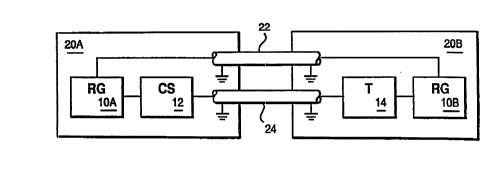
The block diagram of FIG. 1 shows a driver 20A with a reference
generator 10A ~roviding a reference signal to a current source 12. The
current source is connected to one end of a transmission line 24 having a
predetermined impedance. At the other end of the transmission line 24 is
a second driver 20B with its own reference generator 10B ~roviding a
reference signal to an active terminator 14. The reference generators 10A
and 10B are interconnected by a re~erence line 22. The driver 20A
reference generator 10A reference signal to the current source 12 sets a
certain magnitude for a current signal which the current source 12 sends
to the receiver 20B over the transmission line 24. The receiver 20B
reference generator 10s re~erence signal to the terminator 14 sets a
family of impedances for the termination of the transmission line 24 at
the transmission line ter~;n~tor 14 such that for the current signal
magnitude set by the driver reference generator 10A the terminator 14
impedance matches the im~edance of the transmission line 24. The
reference generators 10A and 10B set the im~edance family and the current
magnitude interactively and continuously using the feedback path of the
reference line 22.
FIG. 2 shows another embodiment having the elements of the
: '-o~m~nt of FIG. 1 and additional elements. FIG. 2 shows reference
generator 10, switched current source 12, active t~rm;n~tor 14, multidro~
receiver 16 and logic circuit 18 in a first and second driver/receiver 20.
The reference generators 10 are interconnected by a single reference line
22 with a grounded shield. The reference line 22 feeds back a common
reference signal between the driver/receivers 20 which is generated by the
reference generators 10. A reference generator 10 in a driver/receiver 20
also generates re~erence signals which are fed to the switched current
source 12, active terminator 14 and receiver 16 in the driver/receiver 20.
The switched current source 12, active t~rm;n~tor 14 and receiver 16 in a
driver/receiver device 20 are connected to an end of a transmission line
24 for carrying logic signals between driver/receiver devices 20. The
tr~nQ~;ssion line 24 also has a grounded shield.
The receiver 16, terminator 14 and switched current source 12 in a
driver/receiver device 20 are connected to the logic circuit 18 for the
device. The logic circuit 18 initiates generation of current ~ulses
representing logic signals in the switched current source 12 for
trAn~1ssion over the transmission line 24 between the driver/receiver
devices 20. The logic circuit 18 also receives logic signals detected by
the receiver 16 or the terminator 14, ~rom signals the receiver 16 or
t~- 1n~tor 14 measures on the transmission line 24. The logic circuit 18
al80 ~rovides mode select signals to the current source 12, receiver 16,
CA 022l6367 l997-09-24
W O 96/36114 PCT/GB96/00405
and tPrmtnAtor 14, for selecting between the source 12 ~roviding a fixed
magnitude logic signal current or a current of variable magnitude which
matchles transmission line 24 impedance, and for switching the tPr~;n~tor
14 in a device 20 on or off.
The reference signals generated by the reference generator 10
control the ;m~e~Ance in ~he ,~r~ n-tor lA, the .m..~litudP- of transmitted
current ~ulses representing logic signals generated in the current source
12, and the amplitude of voltage pulses which the multidrop receiver 16 or
term;n~tor 14 detects as logic signals in signals received on the
tra~smission line 24. ThiS common reference line between the
driver/receiver devices 20 allows the devices 20 to establish a common
basis for the parameters controlled by the reference generators 10.
Since the logic signal current transmitted by a driver 20 is varied
by the reference generator lO in the driver 20 in accordance with the
fee~hA~k och~n;sms described above, the signal current or voltage which a
receiver 16 or tprminator 14 measures does not have a fixed magnitude.
Therefore, the receiver 16 or tPrm;n~tor 14 uses reference signals from
the refere~e genP-rator 10 for comparison against the signal received on
the t:ransmission line 24 in order to dete ;ne the value of a logic
signal.
Signals received by a driver/receiver 20 on the transmission line 24
may be interpreted either by a multidrop receiver 16 or by a detector in
the tPrm;n~tor 14. AS Will be understood from the descri~tion of the
receiver below, the receiver 16 does not load the transmission line 24.
The receiver 16 is therefore useful for a~plications where many
driver/receiver devices 20 are connected together on a transmission line
24. The tPrm;n~tor 14 is advantageous in that it provides a term;nation
to the tr~n~m;Ssion line 24 which more ~recisely matches the impedance of
the transmission line 24 so that signals can be measured with more
~recision. Since having a number of tPrr;n~tors 14 active on the
transmission line 24 will load down and mismatch the transmission line 24
the invention includes provision for the logic circuit 18 to switch off
the tpr~n~tor 14.
The diagram of FIG. 3 shows another, more detailed block diagram for
one of the driver/receivers 20 of FIG. 2. The reference generator 10
~ 40 includes a first and second reference active tP ;n~tor 30 and 32, a
differential voltage amplifier 34, a differential current amplifier 36, a
receiver reference voltage generator 38, and a current mirror 40. In
order to focus on the operation of the devices in generating, transmitting
and receiving signals, FIG. 3 omits the logic circuit 18 and logic control
lines shown in FIG. 2.
CA 02216367 1997-09-24
W 096/36114 PCT/GB96/00405
The differential voltage amplifier ("DVA'I) 34 receives a first
voltage input V1 that is the voltage generated by current i1 flowing
through the first terminator 30, including the resistor 20Zo (FIG. 5) and a
second voltage input V2 that iR the voltage across the second t~rm;n~tor 32
generated by current i2 flowing through the second tPrm;n~tor 32. The DVA
34 provides an outPut to the gates of FET's QP0, QP3, QP5, QP6, QP7, and
QPl0 along a rail labeled "IRP" (the "IRP rail FET's"). The DVA 34 output
to the IRP rail sets a certain current in QP5 which is fed back to the DVA
34. An increasing voltage output from DVA causes a decreasing current in
the IRP rail FET~s. The FET~s on the IRP rail mirror the current in QP5.
The term "mirror" a~plies to field effect devices which are well
matched. To "mirror" a current refers to ap~lying the same gate voltage
to matched FET~s and thereby causing the same drain current, or a
predet~n~;n~d matching scaled drain current, in the FET's. Although the
value of the drain current may not be known, since the FET~s match
therefore it is assumed that the drain current will be matching in each
FET, whatever that drain current may be.
The same principles a~ly to bipolar transistors so that these
current mirror circuits could be configured with bi~olar transistors.
There are some differences between field effect and bi~olar devices, but
they do not prevent ~racticing this invention with bipolar transistors.
One difference is that bipolar transistors draw a base current, whereas
FET~s do not draw a gate current. This makes FET~s more desirable for
this application. Another difference is that bi~olar transistors have a
flatter linear region in the drain current versus gate-to source voltage
characteristic. This favors bipolar devices.
By increasing or decreasing its output voltage, DVA 34 increases or
decreases currents i1 and i2 through the reference terminators 30 and 32 in
response to anY difference in the two voltage inputs to DVA so that the
currents il and i2 through the t~rm;n~tors 30 and 32 will increase and
decrease the voltages across the t~rm;nators 30 and 32. Ultimately a
certain combination of the currents i1 and i, produces a substantially
equal voltage dro~ across the t~rm;nators 30 and 32 and thus satisfies the
DVA 34.
The differential current amplifier ("DCA") 36 receives a first
current input from the second terminator. The input is a current that
mirrors the current i2 set by the DVA 34 through the second terminator 32.
The DCA 36 also receives a second current input from FET QPl0 on the IRP
rail. Since QPl0 matches QP5 and QP3, and since the DVA output ~rovides
the gate voltage to QP3, QP5 and QPl0, the voltage output from DVA 34 sets
a current through QPl0 that is the same as current i1.
CA 02216367 l997-09-24
WO ~6136114 PCT/GB96/00405
This current through QP10 i5 compared by the DCA 36 to the first
current input. The DCA 36 ~rovides an out~ut signal that adjusts the
;m~e<lAnre of both of the reference terminators 30 and 32 to cause all the
current through QP0 to go into the second t~;nAtor 32 80 that no current
flows through the reference line 22 into or out of the node between QP0
and the second terminator 32.
The reference line 22 between the reference generators 10 at each
end of the transmission line 24 forces each seCond t~rm;n~tor 32 on the
ends of the transmission line 24 to have the same voltage dro~. And, as
just described, the DVA 34 in a reference generator 10 forces the voltage
drop across the reference generator's ~irst terminator 30 to substantially
equal the voltage drop across its second t~ nAtor 32. Thus, both
reference terminators 30 and 32 in both reference generators 10 shown in
FIG. 1 have the same voltage drop.
The current mirror 40 of the reference generator 10 provides a
voltage output IRN to the switched current source 12 and the receiver 16
for driving another matched FET to mirror the current il.
The switched current source 12 hown in FIG. 3 provides a bias
current of magnitude il that is set by the IRP rail voltage from the
reference generator 10, and a signal current of magnitude 20i1 that maybe
set by the current mirror 40 olltput voltage IRN from the reference
25 generator 10. The signal current is switched on or off by the logic
circuit 18. The logic circuit may also select to set the signal current
at a fixed value rather than allowing the signal current to be set by the
reference generator.
The active term;n~tor 14 shown in FIG. 3 has a FET (not shown in
FIG. 3) for tPrm;nAting the transmission line 24. The bias voltage V~, from
the DCA 36 a~Plied to the active t~rm;nAtor 14 adjusts the ;r~re~nre of
the t:e~;n~ting FET to match the impedance of the transmission line 24 at
the particular current which is transmitted by the correspon~l;n~ device 20
at the other end of the transmission line 24. The t~ ;nAtor 14 also has
a detector which compares the signal current flowing in the t~rm;nAtion of
the transmission line to a reference and provides one or more outputs to
the logic circuit 18 indicating the logic value of the signzll current.
The receiver (or llmultidrop receiver") 16 shown in FIG. 3 has a
firs~ in~ut labelled Vr,~r.~ to which the voltage Vr.er.~ from the receiver
re~erence circuit 38 is a~plied, a second input labelled IR~ to which the
voltage IRN out of the current mirror 40 of the reference generator 10 i8
applied, and a third input labelled Vlr, to which the voltage on the
~5 trAn~m; ssion line 24 i8 ap~lied. The signal current sent by the
CA 022l6367 l997-09-24
W 096/36114 PCT/GB96/00405
sender/receiver 20 is set by the feedback m~ n; S~Q in the
sender/receivers such that a logic signal having a current of 20il
correspnn~;n~ to a logic value of 1, combined with a bias current equal to
il, will generate a voltage at the third input v~ equal to Vl, the same as
S the voltage across the reference term;n~tors 30 and 32. The voltage Vin
will transition from a small magnitude generated by the bias current of
magnitude i1 when there is no current signal being sent to the receiver, to
a larger magnitude VflrLl when an additional current signal of magnitude 20
(Corres~nn~;nq to a logic signal 1) is received. When V1~ makes this
transition the receiver 16 output will provide a high signal to the logic
circuit 18 indicating that a logic signal 1 is received.
The reference circuit 38 generates a reference voltage Vr.Cr.f with a
certain correspnnd~n~e to the transmitted signal voltage. The receiver 16
uses Vr.cr.~ for comparison against the signal voltage measured by the
receiver 16 on the transmission line 24 in order to determine the value of
a logic signal. The receiver reference circuit 38 receives a first input,
which is a current that matches the current input to the second reference
terminator 32, and a second input, which is the voltage Vl at the second
reference terminator 32 (and which will be the same as Vl, the voltage at
the first reference terminator 30). From these inputs, reference voltage
Vr.Cr.f is generated for use by the receiver circuit 16 to set a transfer
function for a logic signal received from a device 20 on the transmission
line 24.
DETAILED CIRCUIT DESCRIPTION
The sender/receiver device of the present invention may be achieved
by a variety of circuits, as will be apparent to those skilled in the art
from the above description of the operation of the various portions of the
device. The following is a description of the circuits used in the
preferred embodiment of the invention. The FET's described herein
generally are matching FET's. The invention is not limited to the
relative scaling factors among the FET's described in the following. A
variety of scaling factors may be used to achieve the results described
for the sender/receiver devices. A power sup~ly voltage of magnitude Vdd
is assumed throughout.
FIG. 4 shows a circuit for the DVA 34 in the ~referred embodiment of
the present invention. FET QP5 is connected gate-to-drain in series with
FET QN10. As long as QN10 is in its linear region (i.e., above the knee
of its drain current vs. gate-to-source voltage curve) QN10 acts as a
current sink controlled by the QNl0 gate voltage and sinks a fixed current
regardle~s of the drain-to-source voltage drop across FET QP5. That fixed
current flowing through QP5 drives the gate-to-source voltage in QP5 to
CA 022l6367 l997-09-24
W 096/36114 PCTIGB96/00405
11 '
whatever value is required for the current which QPS sources. The
resulting voltage on the QP5 gate su~plies the gate voltage for all the
FET's on the IRP rail. To the extent that each FET on the IRP rail is
operating within its linear region, since these FET'S match QP5, the
resulting currents through the FET's are in ~Lo~oLLion to the current
through QP5 according to their relative w/L scaling factors. Referring to
FIG. 5, the matched FET'S QPO and QNO have a w/L scaling factor of 21 so
that the current i2 through the second reference tPr~inA~tor 32 is 21 times
the current il through the first reference ter~;nAtor 30. The current of
10 magnitude 21il in the tPrm;nAtor 32 represents current of magnitude 20
generated by current source 12 as a logical signal 1, combined with
current of magnitude il generated by current source 12 as a bias current.
Referring again to FIG. 4, the DvA 34 has a first and second input
lS connected so that the first input measures the voltage V1 across the first
reference terminator 30, and the second input measures the voltage V2
across the second reference tPrm;nAtor 32. The first input voltage biases
FET QN8 tied to the gate of FET QN10. The second input voltage biases FET
QNl, which is mirrored by FET'S QPl and QP4. FET QP4 iS also tied to the
gate of FET QP10. Due to the configuration of the connections of the
FET'-q QNl, QN8, QPl, QP4, and QN10 shown in FIG. 4, if vl increases, the
gate voltage on QN10 decreases, and if v2 increases, the gate voltage on
FET QN10 increases.
FIG. 5 shows a circuit for the reference t~ ;nAtors 30 and 32 of
the ~referred embodiment. The tP ;nAtors 30 and 32 are identical except
that the first tPrm;nAtor 30 has a resistor R0 with resistance 20zo, where
zO is the known transmission line 24 impedance, and the tPrm;nAting FET'S
in the terminators 30 and 32 are scaled to be identical. Terminator 30
30 has a reference current of magnitude il and terminator 32 has a current of
magnitude 21i1. Since the terminators 30 and 32 have identical FET'S and
currents in this 21/1 proPOrtion, the term;nAtors 30 and 32 provide a
static re~resentation of two dynamic states of the transmission line.
The current source 12 in a driver 20A (FIG. 1) iS represented by a
transient of magnitude 20Zoi1 and a static bias resulting from current of
magllitude il in tPrm;nAtor 32. The terminator 14 in a receiver 20s (FIG.
1) is represented by a current of magnitude 21i in tPr~;nAtor 30. These
two dynamic states of the transmission line 24 correspond to (1) the
condition of the t~ ;n~tor 14 with a current of magnitude i1 flowing
through the tPr~;nAtor 14 and (2) the condition of the terminator 14 with
a current of magnitude 21i flowing in the term;nAtor 14. The values of
the resistor R0 and the scaling factors may be varied so that for a
resistor with resistance NZo, a ratio of N:1 is established between the
bias current of magnitude il and the signal current of magnitude Nil. The
CA 02216367 1997-09-24
W 096/36114 12 PCT/GB96/00405
value of N is arbitrary, but will ordinarily be selected for convenient
circuit implementation, such as N=lO, N=20, etc.
Describing the second reference terminator 32 as an example, the
tPrm;n~ting FET QN0 establishes a termination im~edance. QN7 and QN6 gate
the termination FET QN0 on and off, and when QN0 is on QN7 and QN6 provide
a voltage divider and a bias voltage to establish the family of drain-to-
source t~rm;n~tion i~red~nces for the drain current through the
tPrm;n~tion FET QN0. That is, within a family of impe~nrP~ set by the
bias voltage, for a certain drain current a certain tPr~;n~tion lmre~n~e
is set.
FIG. 6 shows a circuit for the DCA 36 of the preferred embodiment.
The current i, through QN0 of the second reference terminator 32 (FIG. 5),
scaled down by a factor of 21, is mirrored in the DCA 36 FET QN9 by
matching the characteristics of QN9 and QN0, scaling down the W/L of FET
QN9 in comparison to FET QN0, and connecting the gate of QN9 to the gate
of QN0. Thus, QN9 will sink a scaled down current that matches the
current in QN0, and, provided that the load on the drain o~ QN9 must
remain within a range for which QN9 operates in its linear region, QN9
will sink this current regardless of the voltage caused by the current
across the load QP8.
With the gate of QP8 tied to its drain, the QN9 drain current will
drive the source-to-drain voltage across QP8 to whatever value is re~uired
by QP8 to source that current, and the QP8 gate voltage will follow. The
QP8 gate voltage, being connected to the gate of QP9, will set a current
through QP9. Since QP9 matches QP8, the current sources by QP9 will match
the current sunk by QN9.
M~nwh; le, QPlO is forced by the IRP voltage, set by the DVA 34 as
previously described, to source a current having a magnitude of i1 because
the current matches the current i2 through QP0, scaled down by a factor of
21 due to matching the characteristics of QPlO and QP0, scaling down the
W/L of FET QN9 in com~arison to FET QN0, and connecting the gate of QPlO
to the gate of QP0. With its gate tied to its drain, QNl2 is forced to
sink the current i1 sourced by QPlO, and the gate voltage of QNl2 follows.
QNl2's gate voltage being tied to the gate of QNll forces QNll to sink i1.
Thus, the operation of the DCA 36 may be understood as follows. FET
QN0 of the second reference term;n~tor 32 sinks (l) the current i2 sourced
by QP0 driving the second reference t~r~;n~tor 32, combined with (2)
current from the reference line. Also, FET QP9 of the DCA is driven to
source a current which is a scaled down match of the current which FET QN0
is sinking. And, FET QNll is driven to sink a current which is a scaled
-
CA 022l6367 l997-09-24
W 096/36114 PCTIGB96/0040
13
=
down match of the current sourced by QP0. The only way the current
sourced by FET QP9 will equal the current sunk by FET QN11 iS for FET QN0
to sink all the current which FET QP0 sources. To achieve this
equivalence, the voltage Vb on the drains of QP9 and of QN11 provides a
fee~ha~k signal to the gate of QN7 which biases QN0 and adjusts the QN0
impedance.
FIG. 8 shows a circuit for the current mirror 40 in the reference
generator 10 of the preferred embodiment. This Current mirror 40 provides
a voltage output IRN to the switched current source 12 of FIG. 9 and the
receiver 16 of FIG. 11 for driving another matched FET to mirror the
current il. The voltage output from the current mirror 40 is set by the
DVA 34 output driving the matched FET QP7 on the IRP rail to source a
current i1. The current il drives FET QN15 to sink il and the FET QN15
gate voltage follows. This QN15 gate voltage is the IRN voltage output
from t:he reference current mirror ~0. Since QP7 is a p-tYpe FET and QN15
is an n-type FET, IRP decreases and IRN increases relative to ground for
an increasing il.
FIG. 9 shows a circuit for the switched current source 12 of the
preferred embodiment which mirrors the il current set by the reference DVA
34 (FIG. 4) as controlled by the logic circuit 18. The IRN voltage output
from the reference current mirror 40 (FIG. 8) drives the switched current
source 12 FET QN1 to sink il. FET QP1 is forced to source a current to
match the current il sunk by QN1 since QP1 is connected to source the
current sunk by QN1 and since QP1 is connected gate-to-drain. Since the
gate of QP1 is tied to the gate of a FET QP0, and QP0 has matching
characteristics with a 20x scale factor, QP0 mirrors a current that is
twenty times il. Thus, FET QP0 provides a current of magnitude 20il which
re~resents a logic signal 1. Also a bias current of magnitude il is
provided by FET QP100 controlled by the IRP voltage output from the
reference generator 10 DVA 34.
Since QP0 is large, it has a large gate-source charging capacitance,
which is 810W to charge and delays the switching of QP1. Since the
switching time for a FET is dependent u~on the switching voltage level
ap~lied to the gate of the FET, one fast way to charge the gate-source
capacitance and speed up switching time is to connect a FET gate direct to
the rail. Ordinarily this is ap~ropriate, when logic signal levels are
not variable and are set at the full rail voltage. However, in the
~resent application it is desired to vary the logic signal level to match
the signal levels and impe~nreq of the devices on the line. Therefore,
the circuit shown in FIG. 9 is used to switch QP0 quickly while still
setting the current which QP0 sources to a selected level which is less
than a current set by the full rail voltage.
CA 02216367 1997-09-24
W 096/36114 PCT/GB96/00405
14
QNl and QN2 have a constant vgs input '~ IRN~ ~rom reference generator
10 (FIG. 3). IRN sets QNl and QN2 to sink a desired current. Since QP0
proportionately mirrors the QPl current, the current in QNl sets the
signal logic level in QP0 when QPl sources the current sunk by QNl,
~rovided, however that the ~CS~ input to gate NOR0 must remain high so
that the NOR0 output remains low and QN8 therefore remains off. If the
CS input to NOR0 iS set low, then instead of being set by IRN the current
signal sourced by QP0 will be set to a m~;mllm by the rail voltage.
Describing now the variable current mode of operation, wherein the
CS in~ut is set high, initially, with the CS in~ut high and current source
"Data~l input low, QP3 iS on hard, i.e., with QP3 gate tied directly to the
rail, so that QP3 sources the current for QNl and shunts off QP0, QPl, and
QP2. with QP2 off, QN2 vd is low. Gate NORl, with inputs QN2 Vd low and
the inverted l'Data~ input high, thus has a low out~ut turning off QN4.
The Data input is set high to drive QP0 to source the current set by
in~ut IRN. Data input going high immediately switches QP3 off and also
forces the NORl output high. NORl output going high turns on QN4 hard.
That is, the NORl output provides a full rail voltage to the gate of QN4
to switch QN4 faster than would occur if the lower voltage level of IRN
were a~plied to the QN4 gate. QP0, QPl and QP2 are thus turned on quickly
through QN4, and the drain currents in QP0, QPl and QP2 begin to increase.
As the currents reach and begin to exceed the level set by IRN, the drain
voltage going high on QN2 drives the NORl output low, turning off QN4.
With QN4 no longer sinking the current in QP0, QPl and QP2 the current
stops rising and settles at the level set by the matching FET'S QNl and
QN2 as determine~ by IRN.
Once the signal current is set high, it may be switched low by
setting the Data input low. The Data input going low ; mm~ tely switches
QP3 on hard, which quickly turns off QP0, QPl and QP2. U~on turning off
QP2, the NORl input from the drain voltage on QN2 goes low.
Repeating the above analysis for the case where the CS in~ut is set
low, it will be understood that setting the CS in~ut low causes the
current ~ource to operate rail to rail, instead of sending a selected
current level det~rm;ne~ by IRN. Initially, with the CS input low and
current ~ource "Data" input low, QP3 iS on hard, i.e., with QP3 gate tied
directly to the rail, so that QP3 sources the current for QNl and shunts
off QP0~ QPl, and QP2. With QP2 off, QN2 vd is low. Gate NORl, with
in~uts QN2 Vd low and the inverted "Data" input high, thus has a low
output t~lrnin~ off QN4. Likewise, gate NOR0~ with inputs CS low and the
inverted ~Data" input high, thus has a low output tllrning off QN8.
~=
CA 02216367 1997-09-24
W 096136114 PCT/GB96/00405
The Data input is set high to drive QP0 to source a current. Data
in~Ut going high ; ?~; ~tely switches QP3 off and also forces the NOR0 and
NORl outputs high. NORl output going high turns on QN4 hard. NOR0 output
going high turns on QN8 hard. QP0, QPl and QP2 are thus turned on quickly
through QN4 and QN8, and the drain currents in QP0, QPl and QP2 begin to
increase. A8 the currents reach and begin to exceed the level set by IRN,
the drain voltage going high on QN2 drives the NORl output low, turning
off QN4. In the variable signal current level mode of operation described
above, when QN4 stops driving the current in QP0, QPl and QP2 the current
StOps rising and settles at the level set by QNl and QN2 as determ;ned by
IRN. However, in the rail to rail mode QN8 is not affected by the current
level set by IRN. Instead~ in the rail to rail mode QN8 stays on as long
as the Data input is high, so that the current in QP0, QPl and QP2
cnnt;n~es to rise to a level set by the rail voltage.
Once the signal current is set high, it may be switched low by
setti.ng the Data in~ut low. The Data input going low ; m~~~; A tely forces
NOR0 out~ut to go low, turning off QN8. Also, the Data input going low
~ tely switches QP3 on hard, which ~uickly turns off QP0, QPl and
QP2. Upon turning off QP2, the NORl in~ut from the drain voltage on QN2
goes low.
FIG. l0 shows a circuit for the active tPrm;nAtor 14 of the
preferred embodiment. The active term;n~tor 14 of receiver 20B (FIG. l)
has an FET QN0 that matches the FET QP0 of the current source 12 of driver
20A ~FIG. l) for sinking the current sourced by QP0 of the driver 20A,
provided that QN0 is connected drain to gate by QN6 being turned on. FET
QN5 is tied to the gate of FET QN0 and receives its gate voltage from the
Vb output of the DCA 36 (FIG. 6). As in the reference terminators 30 and
32 of FIG. 5, vb biases the impedance of the terminating FET. In the case
of the active term;n~tor 14 of FIG. l0, the terminating FET is FET QN0.
In the detector portion of the terminator 14, the gate of FET QMl is
connected to the gate of terminator FET QN0 to mirror the current through
QN0. FET QPl0l is connected to source whatever current Q~l is driven to
sink, and the gate voltage of QPl0l is connected to FETs QPl02 and QPl03
so that QPl02 and QPl03 also mirror the current according to their scale.
QPl0:3 and QNl03 are sized so that when a current of magnitude 2li1/2 is
sunk through QN0 of the t~rm;n~tor, QPl03 overdrives QNl03 so that QNl03
drain voltage goes high. This QNl03 drain voltage is used as an output to
indicate that a logic signal l is received. QPl02 and QNl02 are sized so
that when terminator FET QN0 sinks a current of magnitude 2li1,
correspnn~;ng to receiving two logic l signals simultaneously, QPl02
overdlives QNl02 and QNl02 drain voltage goes high. FET QNl02 drain
CA 022l6367 1997-09-24
W 096t36114 PCT/GB96/00405
16
voltage i9 used as an out~ut to provide an indication that two logic 1
signals have been received simultaneously.
FIG. 7 shows a circuit for the receiver reference circuit 38 of the
~referred embodiment. The receiver reference circuit 38 receives a
current set by the DVA 34 output ap~lied to the gate of a matched FET QP6
so that the current input irr to the receiver reference circuit 38 matches
the current input i2 to the second reference terminator 32. The current
irr drives FET QN13, while at the same time the voltage V2 at the second
reference terr;n~tor 32, and which is a~plied as the second in~ut to the
DVA 34, is a~plied to the QN13 gate. The current irr driving FET QN13 is
sunk by FET QN14 connected as a cascade pair with QN13. The gate of FET
QN14 is tied to the drain of QN13 and provides a reference voltage Vr.Cr.f,
which iR the voltage required at the gate of one of the FET~s of the
caRcade FET pair to sink current irr, where the voltage at the gate of the
other FET of the pair is the voltage V~ at the second reference terminator
32. This voltage Vr.cr.~ is used by the receiver circuit 16 to set the
transfer function of QN9 and QN10, so the voltage transition on V1n will
create a known current transition through QP5. This current transition is
generated to have a magnitude of il at the transmission line 24 voltage
V~". FET~s QP6 and QN11 ~rovide a current comparator which generates a
voltage of magnitude Vd~ indicating a logic signal 1 when the current in
QP5 exceeds a magnitude of il/2. QN11 i8 sized to sink a current of
magnitude il/2 at the IRN voltage.
FIG. 11 shows a circuit for a multidrop receiver 16. The multidro~
receiver 16 has a pair of FET's QN9 and QN10 which match the FET~s QN13
and QN14 in the receiver reference circuit 38. The reference voltage Vr.cr.
generated by the receiver reference circuit 38 is a~lied to the gate of
FET QN10 in the receiver 16. The transmission line 24 voltage V1n is
applied to the gate of FET QN9 in the receiver 16. Since FET's QN9 and
QN10 match the cascade pair QN13 and QN14 in the receiver reference
circuit 16, and QN10 gate has Vr.Or~ ap~lied, FET's QN9 and QN10 will sink a
current that matches current i1 when the voltage applied to the gate of QN9
is the same as the voltage Vl a~plied to the reference tPrm;n~tors 30 and
32. The signal current sent by the sender/receiver 20 is set by the
feedback mP~h~n;! g in the sender/receivers such that a logic signal
having a current of 20il correspon~;ng to a logic value of 1, combined with
a bias current e~ual to i" will generate a voltage e~ual to Vl at the gate
of QNg.
FET QP5 is connected in series with FET~s QN9 and QN10, with the
gate of QP5 connected to its drain so that QP5 sources the current that
QN9 and QN10 sink. FET QP6 is connected to mirror the current sourced by
~5 FET QP5. FET QP6 is in series with an FET QN11 which is driven by the
CA 022l6367 l997-09-24
W 096/36114 PCT/GB96/00405
17
voltage out of the current mirror 40 of the reference generator 10. FET
QN11 is scaled to sink a current of magnitude 0.5il when driven by a gate
voltage from the current mirror 40 that corresponds to a current of
magnitude i1 in the current mirror 40.
The voltage Vl~ will transition from a small magnitude generated by
the bias current of magnitude il when there is no current signal being sent
to the receiver 16, to a larger magnitude (referred to as V~ ) when an
additional current signal of magnitude 20il (corresp~n~;ng to a logic
signal 1) is received. When v1n makes this transition QP6 will overdrive
QN11 and the voltage on the node between QP6 and QNll will drive to vad.
This node voltage is an output ROut, and provides a detector signal to
logic circuit 18 that indicates a logic signal 1 is received by the
receiver 16.
THEORY OF OPERATION
The theory of o~eration is as follows. The DVA 34 (FIG. 3) sets
reference currents of magnitude il through the first reference tprm;nAtor
30 and, if the transmission line terminator 14 is switched on, as a bias
current through the transmission line termin~tor 14 tPr~;nAting FET QN0
(FIG. 10). DVA 34 also sets a current of magnitude 20il as the signal
current through the current source 12 FET QP0 (FIG. 9). This current 20i1
+ il iS sent onto the transmission line 24 and, if the term~nAtor 14 is on,
the current divides between the t~rm;nAtor 14 and the transmission line
24. DVA 34 also sets a current of magnitude 21il into the node between the
second reference terminator 32 and the reference line 22. The value of
the current il is set by the DVA 34 such that the currents into the
reference terminators 30 and 32 produce voltage drop that are
substantially e~ual.
MPAnwh;le~ the DCA 36 (FIG. 3) sets a bias voltage Vb a~lied to the
reference tP ;nAtors 30 and 32 and the transmission line tPrm;n~tor 14,
which affects the transconductance (and the impedance) of tPrm;n~Ation
FET~s QN0 and QN3 in the first and second reference terminators and the
tPrm-n~tion FET QN0, in the transmission line terminator 14 (FIG. 10) such
that the current of magnitude 21il set by the DVA flows into second
reference tprm;nAtor 32 (i.e., no current flows into the reference line
22).
~ 40
DVA 34 and DCA 36 interact, in that the current magnitudes set by
DVA 34 affects the current that flows into the reference tPr~;nAtors 30
and 32 to which the DCA 36 responds, while the bias voltage set by DCA 36
affects the voltage across the reference terminators 30 and 32 to which
the DvA 34 res~onds. The interaction of the DVA 34 and the DCA 36,
CA 022l6367 l997-09-24
WO 96/36114 18 PCT/GB96/00405
together with the matching characteristics of the FET~s in the devices 20
and the selection of scaling factors for the FET~s and resistors in the
devices 20, forces an equilibrium wherein the reference current il and the
transconductance of FBT QN0 satisfies the equation:
20ilzO 1 i = 21i
~ K L
which results in matching the impedance of the transmission line 24 with
that of the transmission line tPrm;nAtor 14 tP ;n~ting FET QN0 with a
current of magnitude 21i flowing in the FET QN0.
A variable level bias current may be sourced by QP100, as set by IRP
from ref. gen. 10 (FIG. 3). When switched on, the variable level signal
current sourced by QP0 is combined with the bias current at the
transceiver/line node (labelled Iout in FIG. 9). Referring now to FIG. l,
if there is no enabled transmission line ter~;n~tor 14 in a sending device
20A with a current source 12, then all of the combined current is sent
onto the line 24 for a receiving device 20B thereon. Referring to FIG. 2,
if there is an enabled transmission line tPr~;n~tor 14, then the combined
current at the transmitting device 20A divides, a ~ortion of the current
being delivered onto the line and a r: ~;n;n~ portion being delivered to
the tPrrinAtor 14 (not shown) at the transmitting device 20A. Regardless
of whether a transmission line terminator 14 is included in any particular
embodiment o~ the invention, or whether any such ter~;n~tor 14 is enabled,
a multidrop receiver 16 may be included in each transceiver, since the
receiver 16 is connected to the line by its FET QN9 gate, and therefore
does not load the line.
With terminating FET'S QN0 in term;n~tors 14 in each of two devices
20A and 20B on the line 24, and with the ter~;n~ting FET~s having
imped~n~Ps adjusted for the line impedance and the level of transmission
currents, the current at a transmitting device 20 divides equally between
the term;n~tor 14 and the line 24. Thus, with one half of a transmitted
current being sent from a first device 20A to a second device 20B, and one
half being delivered to the first device 20A~s own terminator 14, and with
one half of a transmitted current being sent from a second device 20B to a
first device 20A, and one half being delivered to the seCond device 20B's
own tPrmin~tor 14, when both devices 20A and 20B send a certain equal
level of current, ~ay 21il, a device's tPr~n~tor 14 will receive that
level, 21il. When only one device 20 sends a current 21i, each device 20
receives 0.5~21il, regardless of which device 20 sends. And, of course,
when neither device 20 sends a signal current, then only a bias current of
O . 5 il i8 received by each device 20.
CA 022l6367 l997-09-24
WO 9~/36114 PCT/GB96/00405
19
Referring now to FIG. 10, the terminating FET QN0 of the
transmission line term;n~tor 14 is switched in and out of the circuit by a
logic signal to the gate of QN6. with QN6 turned off (as controlled by
logic circuit 18 in FIG. 2) QN0 is turned off, unloading the line and
disabling the terminator 14. with QN6 turned on, the t~rm;n~tor 14 is
enabled and QN0 provides a variable impedance sink set by bias voltage Vb
to the gate of QN5 for sinking a current applied at the transceiver/line
node (''Iout~l in FIG. 10). The current received by QN0 is mirrored to FET
QM1 and converted to logical data by the detector circuit formed by FET's
QM1, QP101, QP102, QN102, QP103, and QN103 as described elsewhere herein
so that both of the COMP1 and COMP2 outputs is high when a current of
level 211 is received, one output is high when a current of level 0.5~211
is received, and neither output is high when no current is received. This
data may be combined with data from the receiving device indicating
whether the device transmitted a portion of the received signal in order
to detl~rm~ne what portion of the received signal was transmitted
externally. This may be ex~ressed in a table as follows:
~ v~ ~ ca~ cc~ v~
2 0 .,.. 3~ T T~
211 Y H H
211/2 Y . L H O
211/2 N L H
25 ~l N L L O
As the above analysis illustrates, according to the present
invention two transceivers 20 with enabled transmission line terminators
30 14 may simultaneously transmit and receive data between the two
transceivers 20 over a single line 24. And, also according to the present
invention, the t~ ;n~ting impedance of a first transceiver 20, and the
level of current Iout for a logic signal, may be controlled to match the
line 24 ;mretl~nre, and the t~rm;n~ting impedance and logic current level
35 of a second transceiver 20 using solely a single reference line 22. And,
regardless of whether an enabled transmission line terminator 14 is
included, the mode of operation of the current source 12 of the present
invention may be selected as a rail to rail current driving mode or a mode
having variable current level. In the variable mode, the signal level of
40 a number of transceivers 20 may be matched, using solely a single
reference line 22 between the devices 20.