Note: Descriptions are shown in the official language in which they were submitted.
CA 02216434 2002-05-22
-1-
ARCING FAULT DETECTION SYSTEM
FIELD OF THE INVENTION
The present invention relates to the protection of electric circuits and, more
particularly, to the detection of hazardous arcing faults typically ignored by
conventional circuit interrupters.
BACKGROUND OF THE INVENTION
The electrical systems in residential, commercial and industrial applications
usually include a panelboard for receiving electrical power from a utility
source. The
power is then routed through overcurrent protection devices to designated
branch
circuits supplying one or more loads. These overcurrent devices are typically
circuit
interrupters such as circuit breakers and fuses which are designed to
interrupt the
electrical current if the limits of the conductors supplying the loads are
surpassed.
Interruption of the circuit reduces the risk of injury or the potential of
property
damage from a resulting fire.
Circuit breakers are a preferred type of circuit interrupter because a
resetting
mechanism allows their reuse. Typically, circuit breakers interrupt an
electric circuit
due to a disconnect or trip condition such as a current overload or ground
fault. The
current overload condition results when a current exceeds the continuous
rating of the
breaker for a time interval determined by the trip current. The ground fault
trip
condition is created by an imbalance of currents flowing between a line
conductor and
a neutral conductor such as a grounded conductor, a person causing a current
path to
ground, or an arcing fault to ground.
Arcing faults are commonly defined as current through ionized gas between
two ends of a broken conductor, between two conductors supplying a load, or
between a conductor and ground. A major problem results from arcing faults
which
do not cause the circuit breaker to trip. Arcing fault current levels may be
reduced by
branch or load impedance to a level below the trip curve settings of the
circuit
CA 02216434 2002-05-22
-2-
breaker. In addition, an arcing fault which does not contact a grounded
conductor or
person will not trip a ground fault protected circuit.
There are many conditions that may cause an arcing fault. For example,
corroded, worn or aged wiring or insulation, loose connections, wiring damaged
by
nails or staples through the insulation, and electrical stress caused by
repeated
overloading, lightning strikes, etc. These faults may damage the conductor
insulation
and reach an unacceptable temperature. Arcing faults can cause fire if
combustible
materials are in close proximity.
There are also many conditions that may cause a "false" arcing fault. For
example, the occurrence of an arcing fault event in one branch circuit of an
electrical
distribution system often causes a false arcing fault signal in another branch
circuit as
a series path is created between the branch circuits through a load center. As
a result,
circuit interrupters in more than one branch circuit are erroneously tripped.
Another
example is a noisy load such as an arc welder, electric drill, etc. producing
a high
frequency disturbance in the electrical circuit which appears to be an arcing
fault.
SUMMARY OF THE INVENTION
It is desirable to provide an arc fault detection system and method which
reliably detects arc fault conditions ignored by conventional circuit
interrupters.
It is further desirable to provide an arc fault detection system which can be
conveniently retrofitted into existing residential, commercial and industrial
facilities
at minimal cost.
It is additionally desirable to provide an arc fault detection system and
method
which distinguishes between hazardous arc faults and normal operation of
equipment
or household appliances, as well as noisy loads, using the electrical circuit.
It is also desirable to provide an arc fault detection system which
electrically
isolates multiple branch circuits in an electrical distribution system.
In accordance with one aspect of the present invention there is provided a
method of detecting arcing faults in an electrical distribution system that
includes a
line conductor connected to a utility power transformer, the method including:
CA 02216434 2002-05-22
-3-
monitoring the rate of change of electrical current in the line conductor and
producing
a signal representing the rate of change, producing a pulse each time the rate-
of
change signal exceeds a selected threshold, filtering at least one of the rate-
of change
signal and the pulses to substantially eliminate signals or pulses
representing changes
in the electrical current outside a selected frequency range while preserving
unfiltered
signals or pulses representing changes in the electrical current within the
selected
frequency range, producing a signal representing a number of the unfiltered
signals or
pulses occurring within a selected time interval; and generating au arc-fault-
detection
signal in response to signal representing number of unfiltered signals or
pulses
occurring within a selected time interval exceeding a trip threshold level.
Other aspects and features of the present invention will be apparent to those
skilled in the art from the present specification taken with the accompanying
drawings
and appended claims.
BRIEF DESCRIPTION OF THE DRAWINGS
In the drawings:
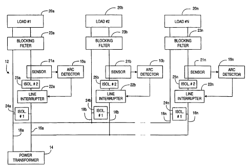
FIG. 1 is a block diagram of an arc fault detection system embodying the
present invention;
FIG. 2 is a schematic diagram of an electrical circuit for implementing the
arc
fault detection system illustrated in FIG. 1;
FIGS. 3a through 3g are waveforms at various points in the circuit of FIG. 2;~
CA 02216434 1998-04-14
WO 97130501 PCT/US97J01869
FIG. 4 is a schematic diagram of an alternative circuit for use in place of
the
comparator and single-shot pulse generator in the circuit of FIG. 2; and
FIG. 5 is a schematic diagram of an alternative circuit for implementing the
fault detection system illustrated in FIG. 1.
DET~.ED DESCRIPTION
Turning now to the drawings and referring first to FIG. 1, arc fault detectors
10a, lOb ... lOn are connected to n branches of an electrical distribution
system 12
having a utility company power transformer I4 as a source of electrical power.
The
electrical distribution system 12 includes line conductors 16a, 16b ... 16n
and neutral
conductors 18a, 18b ... 18n which distribute electrical power to loads 20a,
20b ...
20n through corresponding sensors 21a, 21b ... 21n, line interrupters 22a, 22b
...
22n, and blocking filters 23a, 23b ... 23n. The line conductors 16 and the
neutral
conductors 18 are typically at 240 volts or 120 volts, and a frequency of 60
Hz.
Each of the line interrupters 22 is preferably a circuit breaker which
includes
an overload trip mechanism having a thermal/magnetic characteristic which
trips the
breaker contacts to an open circuit condition in response to a given overload
condition, to disconnect the corresponding load 20 from the power source, as
is
known in the art. It is also known to provide the circuit breaker 22 with
ground fault
interrupter circuitry responding to a line or neutral-to-ground fault to
energize a trip
solenoid which trips the circuit breaker and opens the contacts.
The sensors 21 monitor the rate of change of electrical current in the
respective Iine conductors 16 and produce signals representing the rate of
change.
The rate-of change signal from each sensor 21 is supplied to the corresponding
arc
detector 10, which produces a pulse each time the rate-of-change signal
increases
above a selected threshold. The rate-of change signal and/or the pulses
produced
therefrom are filtered to eliminate signals or pulses outside a selected
frequency
range. 1 ne renal purses are then monitored to detect when the number of
pulses that
occur within a selected time interval exceeds a predetermined threshold. In
the event
that the threshold is exceeded, the detector 10 generates an arc-fault-
detection signal
that can be used to trip the corresponding line interrupter 22.
CA 02216434 1998-04-14
WO 97130501 PCT/LTS97/01869
-5-
The pattern of fluctuations in the rate-of change signal produced by the
sensor
21 indicates whether the condition of the circuit is a normal load, a normal
switching
event, a phase-controlled fired load, or an arcing fault event. One example of
a
suitable sensor for producing the desired rate-of change signal is a toroidal
sensor
having an annular core encompassing the current-carrying load line, with the
sensing
coil wound helicaily on the core. The core is made of magnetic material such
as a
ferrite, iron, or molded permeable powder capable of responding to rapid
changes in
flux. A preferred sensor uses a ferrite core wound with 200 turns of 24-36
gauge
copper wire to form the sensing coil. An air gap may be cut into the core to
reduce
the permeability to about 30. The core material preferably does not saturate
during
the relatively high currents produced by parallel arcs, so that arc detection
is still
possible at those high current levels.
Other means for sensing the rate of change of the current in a line conductor
are contemplated by the present invention. By Faraday's Law, any coil produces
a
voltage proportional to the rate of change in magnetic tux passing through the
coil.
The current associated with an arcing fault generates a magnetic flux around
the
conductor, and the coil of the sensor 21 intersects this flux to produce a
signal.
Other suitable sensors include a toroidal transformer with a core of magnetic
material
or an air core, an inductor or a transformer with a laminated core of magnetic
material, and inductors mounted on printed circuit boards. Various
configurations for
the sensor core are contemplated by the present invention and include toroids
which
have air gaps in their body.
Preferably, the rate-of-change signal produced by the sensor 2I represents
only fluctuations in the rate of change within a selected frequency band. The
sensor
bandpass characteristic is preferably such that the lower frequency cut-off
point
rejects the power frequency signals, while the upper frequency cut-off point
rejects
the high frequency signals generated in the presence of noisy loads such as a
solder
gun, electric saw, electric drill, or like appliances, equipment, or tools.
The
resulting output of the sensor 21 is thus limited to a selected frequency band
associated with arcing faults, thereby eliminating or reducing spurious
fluctuations in
the rate-of-change signal which could result in nuisance tripping. As an
example, the
sensor bandpass characteristic may have: (1) a lower frequency cut-off point
or
CA 02216434 1998-04-14
WO 97/30501 PCT/US97/01869
-6-
lower limit of 60 Hz so as to reject power frequency signals, and (2) an upper
frequency cut-off point or upper limit of approximately 1 MHz so as to
effectively
reject all high frequency signals associated with noisy loads. These specific
frequency cut-off points for the sensor bandpass characteristic are by way of
example
only, and other appropriate frequency cut-off limits may be adopted depending
upon
actual frequency ranges for the power signals as well as the noisy load
signals.
The desired bandpass characteristic is realized by appropriately selecting and
adjusting the self resonant frequency of the sensor. The current-type sensor
is
selected to have a predetermined self resonant frequency which defines
associated
IO upper and lower frequency cut-off or roll-off points for the operational
characteristics
of the sensor. Preferably, the current-type sensor is designed to exhibit the
desired
bandpass filtering characteristic as it operates to detect the rate of change
of current
variations within the load line being monitored. The present invention
contemplates
other means for bandpass filtering the signal output within the selected
frequency
band. For example, a bandpass filter or a combination of filters in a circuit
can be
used to attenuate frequencies above or below the cut-off points for the
selected
frequency band.
FIG. 2 illustrates a preferred circuit for one of the arc detectors 10. The
sensor 21 produces the desired rate-of-change-of-current signal (commonly
referred to
as a "di/dt signal") in the form of an output voltage which is connected to a
comparator circuit 30 through a filtering network in the sensor and a diode
D3. The
rate-of-change signal originates in the sensor coil T1 which is wound on a
core
surrounding the load line 16. Connected in parallel with the sensor coil T1
are a pair
of diodes D 1 and D2 which serve as clamping devices during high-power
transient
conditions. A resistor R1 in parallel with the diodes D1 and D2 dampens the
self
ringing of the sensor, during high-power transients. A pair of capacitors C 1
and C2
in parallel with the resistor R1, and a resistor R2 and an inductor L1
connected in
series to the input to the comparator 30, are tuned to assist in attaining the
desired
rolloff characteristics of the filtering network formed thereby. For example,
with the
illustrative values listed below for the components of the circuit of FIG. 2,
the sensor
has a passband extending from about 10 KHz to about 100 KHz, with sharp
rolloff at
both sides of the passband.
CA 02216434 1998-04-14
WO 97/30501 PCT/US97101869
The operation of the circuit of FIG. 2 can be more clearly understood by
reference to the series of waveforms in FIGS. 3a through 3g. FIG. 3a is an
actual
waveform from an oscilloscope connected to a line conductor 16 carrying a-c.
power
at 60 Hz and experiencing a high-frequency disturbance beginning at time t1.
Because the high-frequency disturbance is within the frequency range to which
the
sensor 21 is sensitive (e.g., from about 10 KHz to about 100 KHz), the
disturbance
results in a burst of high-frequency noise in the di/dt output signal (FIG.
3b) from the
sensor 21 (at point A in the circuit of FIG. 2), beginning at time t1. The
noise burst
has a relatively high amplitude from time t1 until approximately time t2, and
then
continues at a lower amplitude from time t2 to about time t3.
In the comparator 30, the magnitude of the rate-of-change signal from the
sensor ? 1 is compared with the magnitude of a fixed reference signal, and the
comparator 30 produces an output voltage only when the magnitude of the rate-
of-
change signal crosses that of the reference signal. This causes the detector
10 to
ignore low-level signals generated by the sensor 21. All signals having a
magnitude
above the threshold Ievel set by the magnitude of the reference signal are
amplified to
a preset maximum value to reduce the effect of a large signal. In the
comparator 30,
a transistor Q1 is normally turned on with its base pulled high by a resistor
R3. A
diode D3 changes the threshold and allows only the negative pulses from the
sensor
21 to be delivered to the base of the transistor Q1. When the signal to the
comparator drops below the threshold level (minus 0.2 volt for the circuit
values
listed below), this causes the transistor Q 1 to turn off. This causes the
collector of
the transistor Q1 to rise to a predetermined voltage, determined by the supply
voltage
V~~, a resistor R4 and the input impedance of a single-shot pulse generator
circuit 40.
This collector voltage is the output of the comparator circuit 30. The
collector
voltage remains high as long as the transistor Q1 is turned off, which
continues until
the signal from the sensor 21 rises above the threshold level again. The
transistor Q 1
then turns on again, causing the collector voltage to drop. The end result is
a pulse
output from the comparator, with the width of the pulse corresponding to the
time
interval during which the transistor Q 1 is turned off, which in turn
corresponds to the
time interval during which the negative-going signal from the sensor 21
remains
below the threshold level of the comparator.
CA 02216434 1998-04-14
WO 97/30501 PCTIUS97/01869
_g_
The noise burst in the sensor output is filtered to produce the waveform
shown in FIG. 3c at point B in the circuit of FIG. 2. The waveform at point C
in
the circuit of FIG. 2 is shown in FIG. 3d, and it can be seen that the
amplitude has
been reduced and a d-c. offset has been introduced by summing the filtered
di/dt
signal with a d-c. bias from the supply voltage V« at point C. This is the
input
signal to the base of the transistor Q1.
The output of the transistor Q I is a series of positive-going pulses
corresponding to the negative-going peaks in the input signal. The transistor
output,
at point D in the circuit of FIG. 2, is shown in FIG. 3e. It can be seen that
the
transistor circuit functions as a comparator by producing output pulses
corresponding
only to negative-going peaks that exceed a certain threshold in the filtered
dildt signal
shown in FIG. 3c. At this point in the circuit, the pulses vary in both width
and
amplitude, as can be seen in FIG. 3e.
To convert the output pulses of the comparator 30, which vary in both width
and amplitude, into a series of pulses of substantially constant width and
amplitude,
the comparator output is fed to a single-shot pulse generator circuit 40. This
high-
pass filter circuit includes a pair of capacitors C3 and C.1 connected in
series to the
collector of the transistor Ql, and two resistor-diode pairs connected in
parallel from
opposite sides of the capacitor C4 to ground. The pulses produced by this
circuit
will be described in more detail below in connection with the waveforms shown
in
FIG. 3. The output pulses are predominantly pulses of equal width and
amplitude,
although occasional larger or smaller pulses can result from especially Large
or small
input pulses.
The variable-width and variable-amplitude pulses of FIG. 3e are converted to
a series of pulses of substantially constant width and amplitude by the single-
shot
pulse generator circuit 40. The output of this circuit 40, at point E in the
circuit of
FIG. 2, is shown in FIG. 3f. Although all the pulses shown in FIG. 3f are of
substantially the same size, Larger or smaller pulses may be produced by di/dt
spikes
that are excessively large or excessively small. The vast majority of the
pulses at
point E, however, are substantially independent of the amplitude and duration
of the
corresponding spikes in the di/dt signal, provided the spikes are Large enough
to
produce an output pulse from the comparator 30.
CA 02216434 1998-04-14
WO 97/30501 PCT/US97/01869
-9-
The substantially uniform pulses produced by the circuit 40 are supplied to
the
base of a transistor Q2 through a current-limiting resistor R7. A capacitor CS
connected from the transistor base to ground improves the sharpness of the
roll-off of
the bandpass filtering. The transistor Q2 is the beginning of an integrator
circuit 50
that integrates the pulses produced by the circuit 40. The pulses turn the
transistor
on and off to charge and discharge a capacitor C6 connected between the
transistor
emitter and ground. A resistor R9 is connected in parallel with the capacitor
C6, and
a resistor RS connected between the supply voltage and the collector of the
transistor
Q2 determines the level of the charging current for the capacitor C6. The
magnitude
IO of the charge on the capacitor at any given instant represents the integral
of the
pulses received over a selected time interval. Because the pulses are
substantially
uniform in width and amplitude, the magnitude of the integral at any given
instant is
primarily a function of the number of pulses received within the selected time
interval
immediately preceding that instant. Consequently, the value of the integral
can be
1~ used to determine whether an arcing fault has occurred.
The integral signal produced by the circuit 50 is shown in FIG. 3g, taken at
point F in the circuit of FIG. 2. It can be seen that the integrator circuit
charges
each time it receives a pulse from the circuit 40, and then immediately begins
to
discharge. The charge accumulates only when the pulses appear at a rate
sufficiently
20 high that the charge produced by one pulse is less than the discharge that
occurs
before the ne~ct pulse arrives. If the pulses arrive in sufficient number and
at a
sufficient rate to increase the integral signal to a trip threshold level TR
(FIG. 3g),
SCR/ is triggered to trip the circuit breaker. The circuit is designed so that
this
occurs only in response to a di/dt signal representing an arc fault.
25 When SCR1 is turned on, a trip solenoid S I is energized to disconnect the
load from the circuit in the usual manner. Specifically, turning on SCR1
causes
current to flow from line to neutral through a diode bridge formed by diodes
D7-
DIO, thereby energizing the solenoid to open the circuit breaker contacts in
the line
16 and thereby disconnect the protected portion of the system from the power
source.
30 The d-c. terminals of the diode bridge are connected across SCRl, and the
voltage
level is set by a zener diode D6 in series with a current-limiting resistor
R10. A
varistor V 1 is connected across the diode bridge as a transient suppressor. A
filtering
CA 02216434 1998-04-14
WO 97/30501 PCT/ITS97/01869
- 10-
capacitor C7 is connected across the zener diode D6. The trip circuit loses
power
when the circuit breaker contacts are opened, but of course the contacts
remain open
until reset.
One example of a circuit that produces the desired result described above is
the circuit of FIG. 2 having the following values:
D 1 1N4148
D2 1N4148
D3 1N4I48
D4 1N4148
DS 1 N4148
D6 27v zener
RI 3.01K
IL? 1.3K
R3 174K
R4 27.4K
RS lOK
R6 10K
R7 l OK
R8 4.2K
R9 4.75K
R10 24K
LI 3300uH
L2 SOOuH
L3 SOOuH
C 1 0.OI2uF
C2 .001uF .
C3 .OOIuF
C4 .OOIuF
CS .OOluF
C6 6.8uF
C7 I.OuF
CA 02216434 1998-04-14
WO 97/30501 PCTIUS97/01869
-lI-
C8 I.OuF
Q I 2N2222A
Q2 2N2222A
SCR1 CR08AS-12 made by P~WEREX-Equal
V~~ 27v
Although a circuit breaker is the most commonly used line interrupter, the
output device may be a comparator, SCR, relay, solenoid, circuit monitor,
computer
interface, lamp, audible alarm, etc.
It will be understood that a number of modifications may be made in the
circuit of FIG. 2. For example, the discrete bandpass filter between the
sensor and
the comparator can be replaced with an active filter using an operational
amplifier.
As another example, a single-shot timer can be used in place of the single-
shot pulse
generator in the circuit of FIG. 2. This circuit can receive the output signal
from an
active filter as the trigger input to an integrated-circuit timer, with the
output of the
timer supplied through a resistor to the same integrator circuit formed by the
resistor
R9 and capacitor C6 in the circuit of FIG. 2.
FIG. 4 illustrates a frequency-to-voltage converter circuit that can be used
in
place of all the circuitry between point A and the integrator circuit in FIG.
2. In this
circuit, the signal from point A in FIG. 2 is supplied through a resistor Ra
to a
frequencylvoltage converter integrated circuit 55 such as an AD537 made by
Analog
Devices Inc. The output of the integrated circuit 55 is fed to a pair of
comparators
that form a conventional window comparator. Specifically, the output of the
circuit
55 is applied to the inverting input of a comparator 56 and to the non-
inverting input
of a comparator 57. The other inputs of the comparators 56 and 57 receive two
different reference signals A and B which set the limits of the window, l. e.
, the only
signals that pass through the window comparator are those that are less than
reference
A and greater then reference B.
FIG. 5 illustrates an arc detector 10 for sensing the rate of change of the
line
voltage, i.e., dv/dt, rather than current. The sensor in this circuit is a
capacitor C10
connected between a line conductor 16 and an inductor L10 leading to ground.
The
inductor L10 forms part of a bandpass filter that passes only those signals
falling
CA 02216434 1998-04-14
WO 97130501 PCT/US97/01869
-12-
within the desired frequency band, e.a., between 10 KHz and 100 KHz. The
filter
network also includes a resistor R 10, a capacitor C 1 l and a second inductor
L 11 in
parallel with the first inductor L10, and a resistor RI1 connected between the
resistor
R10 and the capacitor CI1. The resistor R10 dampens the ringing between the
capacitor CI0 and the inductor L10, and the resistor RI1 adjusts the threshold
or
sensitivity of the circuit. The inductors LI0 and L11 provide low-frequency
roll-off
at the upper end of the pass band, and a capacitor C 11 provides the high-
frequency
roll-off at the lower end of the pass band.
The capacitor C 10 may be constructed by attaching a dielectric to the line
buss so that the buss forms one plate of the capacitor. The second plate of
the
capacitor is attached on the opposite side from the buss. The sensor circuit
is
connected to the second plate.
The output of the bandpass filter described above is supplied to a comparator
60 to eliminate signals below a selected threshold, and to limit lame signals
to a
l~ preselected ma.~cimum amplitude. The filter output is applied to the
inverting input of
the comparator 60, through the resistor R1I, while the non-inverting input
receives a
reference signal set by a voltage divider formed by a pair of resistors R12
and R13
connected between V~~ and ground. The comparator 60 eliminates very low levels
of
signal received from the sensor. The comparator 60 is normally off when there
is no
arcing on the line conductor 16, and thus the comparator output is low. When
the
voltage signal from the sensor is more negative than the reference input
(e.g., -0.2
volts), the output from the comparator goes high, and a forward bias is
applied to the
transistor Q2 that drives the integrator circuit. A capacitor C 12 connected
from the
base of transistor Q2 to -V~~ filters out high frequency noise. A diode D 11
is
connected between the comparator output and the base of the transistor Q2 to
block
negative signals that would discharge the capacitor C12 prematurely. The rest
of the
circuit of FIG. ~ is identical to that of FIG. 2.
When a fault occurs, it is desirable to isolate the branch of the distribution
system in which the arcing fault occurred, from the rest of the distribution
system.
In the system of FIG. 1, using the current-type sensor, such isolation is
provided by
a capacitor C8 connected between the load line 16 and the neutral line 18 in
each
branch of the distribution system. The capacitor C8 is located between the
Iine
CA 02216434 1998-04-14
WO 97/30501 PCTIL1S97I01869
- 13-
interrupter 22 and the power source 14 to provide a low impedance path for an
arcing
fault from the load Iine 16 to the neutral line 18, independent of the
impedance of the
load 20. The capacitor C8 thus prevents a series path from being created
between
branch circuits, even though the power transformer 14 appears as a high
impedance
to the high frequency current that an arcing fault generates.
The isolating capacitor C8 allows the sensor 21 to be sensitive even when all
the Ioads are off line and the impedance is high. As the loads come on-line,
the
impedance decreases. Without the isolating capacitor C8, a series path could
be
created between branch circuits. For example, current flow along the neutral
line of
a first branch circuit, within which an arcing fault is generated, could
travel along the
load line of the first branch circuit. The current could then continue the
load line of
a second branch circuit, subsequently flowing along the neutral line of the
second
branch circuit. The isolating capacitor C8 prevents this pathway between
branch
circuits from being formed.
With the voltage-type sensor shown in FIG. 5, isolation is provided by an
inductor L2 in the load line 16 for each branch circuit. Each inductor L2 is
located
between the line interrupter 22 and the sensor 21 to provide an impedance for
the
current produced by an arcing fault.
The isolating capacitors C8 and the isolating inductors L2 may be used
simultaneously in their respective positions in the branch circuits. This
combination
can be particularly useful if the sensors monitor both the current and voltage
changes
in the branch circuits to detect arcing faults. The arcing fault detection
system also
includes a blocking filter 23 in each branch circuit for blocking false arcing
fault
signals or other nuisance output signals generated by normal operation of the
load 20.
Each blocking filter 23 is connected between the sensor 21 and the load 20 in
each
branch circuit to prevent false arcing fault signals from being delivered to
the sensor
21. As seen in Fits. 2 and 5, the preferred blocking filter includes a pair of
capacitors C9a and C9b connected between the Ioad line 16 and the neutral line
18 of
each branch circuit. An inductor L3 is connected in the load line 16 between
the two
capacitors C9a and C9b. Preferably, the capacitors C9a and C9b have a rating
across the line of about 0.47 uF. The inductor L3 has a rating for 15 amps at
500
uH and dimensions of about 1.5" diameter and 1.313" in length (e.g., Dale IHV
15-
CA 02216434 1998-04-14
WO 97/30501 PCT/US97101869
- I4-
500). These values, of course, can be adjusted for the power rating of the
electrical
system and the loads 20.
The capacitor C9a creates a low impedance path for any series arcing that
occurs upstream of that capacitor, such as arcing within the wall upstream of
a noisy
load. This permits series arcing to be detected in the branch containing the
blocking
filter. The inductor L3 creates an impedance that does most of the attenuation
of the
signal created by a noisy load. This inductor is sized to carry the load
current of the
device, which is typically 15 or 20 amperes. The second capacitor C9b reduces
the
amount of inductance required in the inductor L3, by creating a low impedance
path
across the load 20.
One of the advantages of the blocking filter 23 is that it can be used locally
on
a particular branch circuit that is known to connect to a load '_'0 which is
noisy. The
expense of using the blocking filter 23 is reduced since it can be used onlv
where
needed. The blocking filter 23 also allows easy retrofitting to existing
electrical
distribution systems in residences and commercial space.
Although the invention has been described in connection with an ordinary 120
volt system, it is applicable to the voltages of any standard, including 12,
120, 240,
480, 600 and 18500 volts. The invention is suitable for use in residential,
commercial and industrial applications, single-shot or multiphase systems and
at all
frequencies for a-c. as well as d-c. This invention is applicable to
automotive,
aviation, and marine needs, separately derived sources such as generators or
UPS,
and capacitor banks needing incipient fault protection.
Although the present invention has been illustrated with circuit breakers, it
can
also be used with circuit/load monitoring devices, motor monitoring devices,
receptacles, cord plugs, portable diagnostic devices, appliances, switches and
fuses.
One of the many applications of the present invention is its use with ground
fault circuit interrupters (GFCI's). An example of a ground fault interrupter
is a fast
acting circuit breaker that disconnects equipment from the power line when
some
current returns to the source through a ground path. Under normal
circumstances all
current is supplied and returned within the power conductors. But if a fault
occurs
and leaks some current to ground, the GFCI senses the difference in current in
the
CA 02216434 1998-04-14
WO 97130501 PCT/US97101869
- 15 -
power conductors. If the fault level exceeds the trip level of the GFCI, which
is
usually at about 6 mA, the GFCI disconnects the circuit.
Three types of GFCI are commonly available. The first or separately
enclosed type is available for 120-volt, 2-wire and 121240-volt, 3-wire
circuits up to
30 amp. The second type combines a 15-, 20-, 25-, or 30-amp circuit breaker
and a
GFCI in the same plastic case. It is installed in place of an ordinary breaker
in a
panelboard and is usually available in 120-volt, 2-wire, or 120/240-volt, 3-
wire types
which may also be used to protect a 240-volt, 2-wire circuit. The second type
provides protection against ground faults and overloads for all outlets on the
circuit.
A third type having a receptacle and a GFCI in the same housing provides only
ground-fault protection to the equipment plugged into that receptacle. There
are
feed-through types of GFCI which provide protection to equipment plugged into
other
ordinary receptacles installed downstream on the same circuit.
Ground fault equipment is commercially available from the Square D
Company under the catalog designations GROUND CENSOR', HOMELIKE~, QO~
TRILLIANT~ and MICROLOGIC~ ground fault modules. This ground fault
equipment is suitable for protection of main, feeder, and motor circuits on
electrical
distribution systems. It is also usable as ground fault relay and ground fault
sensing
devices. The arc detection systems described above can be advantageously used
to
supplement the circuit protection provided by all the foregoing types of
GFCIs.
The term arcing fault, as used herein, includes faults caused by either series
arcs (both line and neutral) or parallel arcs (line to line, line to ground,
or line to
neutral). The term arc, as used herein, includes not only a discharge of
electricity
through a gas or across an insulating medium, but also high impedance faults
or other
intended or unintended circuit paths which do not have sufficient energy or
current
flow to trip a breaker, but nevertheless can generate damaging heat or other
undesirable effects.
The term mutual inductance, as used herein, is the property shared by
neighboring inductors or inductive devices which enables electromagnetic
induction to
take place. The term rate of current or voltage change, as used herein,
measures the
change in the current or voltage over the period in time corresponding to the
CA 02216434 1998-04-14
WO 97/30501 PCTIUS97/01869
- 16-
measurement. The current generates a flux around the conductor which rapidly
changes with the fluctuations in current.
While particular embodiments and applications of the present invention have
been illustrated and described, it is to be understood that the invention is
not limited
to the precise construction and compositions disclosed herein and that various
modifications, changes, and variations will be apparent from the foregoing
descriptions without departing from the spirit and Scope of the invention as
defined in
the appended claims.