Note: Descriptions are shown in the official language in which they were submitted.
-
CA 02216~7 1997-09-26
W097/28653 PCT~6/00048
-- 1 --
THIN FILM ACTUATED MIRROR ARRAY HAVING DIELECTRIC LAYERS
TECHNICAL FIELD OF THE INVENTION
The present invention relates to an optical
projection system; and, more particularly, to an array of
M x N thin film actuated mirrors for use in the system and
a method for the manufacture thereof, wherein each of the
thin film actuated mirrors is provided with a multilayer
stack of dielectric members successively formed on top of
each of the thin film actuated mirrors to produce an
optimum optical efficiency thereof.
BACKGROUND ART
Among the various video display systems availabLe in
the art, an optical projection system is known to be
capable of providing high quality displays in a large
scale. In such an optical projection system, ligh~ from
a lamp is uniformly illuminated onto an array of, e.g., M
x N, thin film actuated mirrors, wherein each of the
mirrors is coupled with each of the actuators. The
actuators may be made of an electrodisplacive material
such as a piezoelectric or an electrostrictive material
which deforms in response to an electric field applied
thereto.
The reflected light beam from each of the mirrors is
incident upon an aperture of, e.g., an optical baffle. By
applying an electrical signal to each of the actuators,
the relative position of each of the mirrors to the
incident light beam is altered, thereby causing a
deviation in the optical path of the reflected beam from
each of the mirrors. As the optical path of each of the
reflected beams is varied, the amount of light reflected
e 35 from each of the mirrors which passes through the aperture
CA 02216~7 1997-09-26
WO 97/286S3 PCT/KR~''00048
-- 2 -- -
is changed, thereby modulating the intensity of the beam.
The modulated beams through the aperture are transmitted
onto a projection screen via an appropriate optical device
such as a projection lens, to thereby display an image
thereon.
In Figs. lA to lG, there are illustrated
manufacturing steps involved in preparing an array 10 of
M x N thin film actuated mirrors 11, wherein M and N are
integers, disclosed in a copending commonly owned
application, U.S. Ser. No. 08/430,628, entitled 'THIN FILM
ACTUATl~:D MIRROR ARRAY " .
The process for manufacturing the array 10 begins
with the preparation of an active matrix 20 comprising a
substrate 22, an array of M X N transistors(not shown) and
an array of M X N connecting terminals 24.
In a subsequent step, there is ~ormed on top of the
active matrix 20 a thin film sacrificial layer 40 by using
a sputtering or an evaporation method if the thin film
sacrificial layer 40 is made of a metal, a chemical vapor
deposition(CVD) or a spin coating method if the thin film
sacrificial layer 40 is made of a phosphor-silicate
glass(PSG), or a CVD method if the thin film sacrificial
layer 40 is made of a poly-Si.
Thereafter, there is formed a supporting layer 15
including an array of M X N supporting members 30
surrounded by the thin film sacrificial layer 40, wherein
the supporting layer 15 is formed by: creating an array of
M x N empty slots(not shown) in the thin film sacrificial
layer 40 by using a photolithography method, each of the
empty slots ~eing located around the connecting terminals
24; and forming a supporting member 30 in each of the
empty slots by using a sputtering or a CVD method, as
shown in Fig. lA. The supporting members 30 are made of
an insulating material.
In a following step, an elastic layer 70 made of the
CA 022l6~7 l997-09-26
W097t28653 PCT~6100048
-- 3
same insulating material as the supporting members 30 is
formed on top of the supporting layer 15 by using a Sol-
Gel, a sputtering or a CVD method.
Subsequently, a conduit 35 made of a metal is formed
in each of the supporting members 30 by: first creating an
array of M x N holes(not shown), each of the holes
extending from top o~ the elastic layer 70 to top of the
connecting terminals 24, by using an etching method; and
filling therein with the metal to thereby form the conduit
35, as shown in Fig. lB.
In a next step, a second thin film layer 60 made of
an electrically conducting material is formed on top of
the elastic layer 70 including the conduits 35 by using a
sputtering method. The second thin film layer 60 is
electrically connected to the transistors through the
conduits 35 formed in the supporting members 30.
Then, a thin film electrodisplacive layer 80 made of
a piezoelectric material, e.g., lead zirconium
titanate(PZT), is formed on top of the second thin film
layer 60 by using a ~ol-Gel, a sputtering or a CVD method,
as shown in Fig. lC.
In an ensuing step, the thin ~ilm electrodisplacive
layer 80, the second thin film layer 60 and the elastic
layer 70 are patterned into an array of M x N thin film
electrodisplacive members 85, an array of M x N second
thin film electrodes 65 and an array of M x N elastic
members 75 by using a photolithography or a laser trimming
method until the supporting layer 15 is exposed, as shown
in Fig. lD. Each of the second thin film electrodes 65 is
connected electrically to a corresponding transistor
through the conduit 35 formed in each of the supporting
members 30 and functions as a signal electrode in each of
the thin film actuated mirrors 11.
Next, each of the thin film electrodisplacive members
85 is heat treated to allow a phase transition to take
CA 02216~7 1997-09-26
WO 97/28653 rCT/KR9~6J~ 18
- 4 -
place to thereby form an array of M x N heat treated
structures(not shown). Since each of the thin film
electrodisplacive members 85 is sufficiently thin, there
is no need to pole it in case it is made of a
piezoelectric material: for it can be poled with the
electric signal applied during the operation of the thin
film actuated mirrors 11.
After the above step, an array of M x N first thin
film electrodes S5 made of an electrically conducting and
light reflecting material, e.g., aluminum(Al) or
silver~Ag), is formed on top of the thin film
electrodisplacive members 85 in the array of M x N heat
treated structures by first forming a layer 50, made of
the electrically conducting and light reflecting material,
completely covering top of the array of M x N heat treated
structures, including the exposed supporting layer 15,
using a sputtering method, as shown in Fig. lE, and then
selectively removing the layer 50, using an etching
method, resulting in an array 90 of M x N actuated mirror
structures 95, wherein each of the actuated mirror
structures 95 includes a top surface and four side
surfaces, as shown in Fig. lF. Each of the first thin
film electrodes 55 functions as a mirror as well as a bias
electrode in each of the thin film actuated mirrors 11.
The preceeding step is then followed by completely
covering the top surface and the four side surfaces in
each of the actuated mirror structures 95 with a thin film
protection layer(not shown).
The thin film sacrificial layer 40 in the supporting
layer 15 is then removed by using an etching method.
Finally, the thin film protection layer is removed by
using an etching method to thereby form the array 10 of M
x N thin film actuated mirrors 11, as shown in Fig. lG.
There are certain deficiencies associated with the
above described array 10 of thin film actuated mirrors 11
CA 022l6~7 l997-09-26
W097l28653 PCT~WC,~C_~S
-- 5 --
and the method for the manufacture thereof. During the
removal of the thin film protection layer, an etchant used
therein may chemically attack the first thin film
electrode 55, which also functions as a mirror, in each of
the thin film actuated mirrors 11, which may adversely
affect the optical efficiency of the array 10 of thin film
actuated mirrors 11. In addition, the first thin film
electrode 55 may become oxidized, especially when the
first thin film electrode 55 is made of Ag, further
reducing the reflectivity thereof.
DISCLOSURE OF T~E INVENTION
It is, therefore, a primary object o~ the present
invention to provide an array of M x N thin film actuated
mirrors capable of ensuring an optimum optical efficiency
and a method for the manufacture thereof.
In accordance with one aspect of the present
invention, there is provided an array of M x N thin film
actuated mirrors, wherein M and N are integers, for use in
an optical projection system, the array comprising: an
active matrix including a substrate, an array of M x N
connecting terminals and an array of M x N transistors,
wherein each of the connecting terminals is electrically
~5 connected to a corresponding transistor in the array of M
x N transistors; M x N conduits, wherein each of the
conduits is made of an electrically conducting material;
an array of M x N actuating structures, each of the
actuating structures being provided with a connecting and
a light reflecting portions, each of the actuating
structures including an elastic member, a second thin film
electrode, a thin film electrodisplacive member and a
first thin film electrode, wherein each of the conduits is
located at the connecting portion in each of the actuating
- 35 structures, extending from bottom of the second thin film
CA 022l6~7 l997-09-26
W097/28653 PCT~
-- 6 --
electrode to top of the connecting terminal connected
electrically to a corresponding transistor, to thereby
allow the second thin film electrode to function as a
signal electrode in each of the thin film actuated
mirrors, and the first thin film electrode made of a light
reflecting and electrically conducting material is
grounded to thereby function as a mirror and a bias
electrode in each of the thin film actuated mirrors; and
M x N number of multilayer stacks of thin film dielectric
members, each of the thin film dielectric members placed
on top of the light reflecting portion in each of the
actuating structures, wherein said each of the thin film
dielectric members has a predetermined thickness and a
specific refractive index.
In accordance with another aspect of the present
invention, there is provided a method for the manufacture
of an array of M x N thin film actuated mirrors, the
method comprising the steps of: providing an active matrix
including a substrate, an array of M x N connecting
terminals and an array of M x N transistors, wherein each
of the connecting terminals is electrically connected to
a corresponding transistor; depositing a thin film
sacrificial layer on top of the active matrix; creating an
array of M x N empty slots in the thin film sacrificial
layer, each of the empty slots being located around top of
the connecting terminals; depositing an elastic layer made
of an insulating material on top of the thin film
sacrificial layer while filling the empty slots; forming
an array of M x N conduits in the elastic layer, each of
the conduits extending from top of the elastic layer to
top of a corresponding connecting terminal; depositing a
second thin film layer, a thin film electrodisplacive
layer and a first thin film layer successively on top of
the elastic layer, wherein the second thin film layer is
made of an electrically conducting material, and the first
CA 02216~7 1997-09-26
W097/28653 PCT/K~ 8
-- 7
thin film layer is made of an electrically conducting and
light reflecting material; patterning the first thin film,
the thin film electrodisplacive, the second thin film and
the elastic layers, respectively, until the thin film
sacrificial layer is exposed, thereby forming an array of
M x N semifinished actuating structures, wherein each of
the semifinished actuating structures is provided with a
first thin film electrode, a thin film electrodisplacive
member, a second thin film electrode and an elastic
member; depositing a plurality of thin film dielectric
layers successively on top of the semifinished actuating
structures including the exposed thin film sacrificial
layer, each of the thin film dielectric layers having a
predetermined thickness; patterning the plurality of thin
film dielectric layers, respectively, into M x N number of
multilayer stacks of thin film dielectric members, until
the thin film sacrificial layer is exposed again, thereby
forming an array of M x~N semifinished actuated mirrors,
wherein the plurality of thin film dielectric layers are
patterned in such a way that each of the semifinished
actuated mirrors is divided arbitrarily into an actuating
and a light reflecting portions, each of the conduits and
each of the thin film dielectric members being located at
the actuating portion and the light reflecting portion in
each of the semifinished actuated mirrors, respectively;
covering each of the semifinished actuated mirrors with a
thin film protection layer to thereby form an array of M
x N protected actuated mirrors; removing the thin fil~
sacrificial layer; and removing the thin film protection
layer to thereby form the array of M x N thin film
actuated mirrors.
BRIEF DESCRIPTION OF THE DRAWINGS
3~ The above and other objects and features of the
CA 02216~7 1997-09-26
WO 97/28653 PCT/KK9G~ 8
- 8 -
present invention will become apparent from the following
description of the preferred embodiments, when taken in
con~unction with the accompanying drawings, in which:
Figs. lA to lG illustrate schematic cross sectional
views setting forth manufacturing steps for an array of M
x N thin film actuated mirrors previously disclosed;
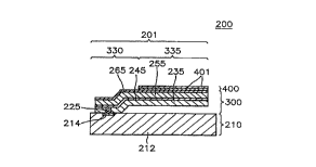
Fig. 2 presents a cross sectional view of an array of
M x N thin film actuated mirrors in accordance with the
present invention; and
Figs. 3A to 3F provide schematic cross sectional
views explaining the present method for manufacturing the
array of M x N thin film actuated mirrors shown in Fig. 2.
MODES OF CARRYING OUT THE INVENTION
Referring now to Figs. 2 and 3A to 3F, there are
provided a cross sectional view of an array 2Q0 of M x N
thin film actuated mirrors 201, wherein M and N are
integers, for use in an optical projection system and
schematic cross sectional views setting forth a method for
the manufacture thereof, respectively. It should be noted
that like parts appearing in Figs. 2 and 3A to 3F are
represented by like reference numerals.
In Fig. 2, there is provided a cross sectional view
of an array 200 of M x N thin film actuated mirrors 201 in
accordance with one embodiment of the present invention,
the array 200 including an active matrix 210, M x N
conduits 225, an array of M x N actuating structures 300
and M x N number of multilayer stacks 400 of thin film
dielectric members 401. For the sake of simplicity, in
Fig. 2, there is shown an array 200 of M x N thin film
actuated mirrors 201, each of the thin film actuated
mirrors 201 having a multilayer stack 400 of thin film
dielectric members 401, wherein the multilayer stack 400
- 35 consists of a pair of thin film dielectric member~ 401.
CA 022l6~7 l997-09-26
W097/28653 PCT/K~G.
_ g _
The active matrix 210 includes a substrate 212, an
array of M x N connecting terminals 214 and an array of M
x N transistors(not shown), wherein each of the connecting
terminals 214 is electrically connected to a correspondin~
transistor.
Each of the actuating structures 300 is provided with
a connecting and a light reflecting portions 330, 335, and
includes an elastic member 235, a second thin film
electrode 245, a thin film electrodisplacive member 255
10 and a first thin film electrode 265. Each of the conduits
225 made of an electrically conducting material is located
at the connecting portion 330 in each of the actuating
structures 300, extending from bottom of the second thin
film electrode 245 to top of a corresponding connecting
15 terminal 214 connected electrically to the transistor,
thereby electrically connecting the second thin film
electrode 245 to the transistor, allowing the second thin
film electrode 24~ to function as a signal electrode in
each of the thin film actuated mirrors 201. The first
20 thin film electrode 265 made of an electrically conducting
and light reflecting material, e.g., Al, is electrically
connected to ground, allowing it to function as a mirror
as well as a bias electrode in each of the thin film
actuated mirrors 201.
Each of the multilayer stacks 400 of thin film
dielectric members 401 is placed on top of the light
reflecting portion 335 in each of the actuating structures
300, wherein each of the thin film dielectric members 401
has a predetermined thickness and a specific refractive
30 index.
In the visible region, it is possible to increase the
reflectance of a simple metal layer by booting it with
extra dielectric layers.
The characteristic reflectance R of a metal in air at
J35 normal incidence is
CA 022l6557 l997-09-26
WO 97/28653 PCT/KI~G~'~~~ 18
-- 10 --
R= 1- [2n/ (l+n2+k2) ] Eq. (1)
1+ [2n/ (l+n2+k2) ]
, wherein n and k are the refractive index and the
extinction coefficient of the metal, respectively.
For example, if the metal is overcoated with two
quarter-waves of material of refractive indices n1 and nz,
n2 being next to the metal, then the optical reflectance
R thereof in air at normal incidence is
R 1-[2 (nl/n2) 2n] / [1+ (nl/n2) 4 (n2+k2) ] Eq. (2)
1+[2 (nl/n2) 2n] / [1+ (nl/n2) 4 (n2+k2) ]
This will be greater than the reflectance of the bare
metal, given by Eq. (1), if
l+(n /n )4(n2+k2) < l+n2+k2 ~q- (3)
, which is satisfied by either
(nl)2>1
or
( n )2< 1 Eq. (4)
CA 022l6~7 l997-09-26
WO 97/28653 PCTlKRg~l~JC_ 1
assuming that n2+kZ 2 1 .
Accordingly to Eq. (4), the reflectance of any metal
can be boosted by a pair of quarter-wave layers for which
(n1/n2)>1, n1 being on the outside and n2 next to the
metal. The higher this ratio, the greater the increase in
the reflectance.
For example, the untreated reflectance of aluminum is
approximately 91.6 % ~or a light beam having a wavelength
of 550nm at normal incidence.
If the aluminum is covered by two quarter-waves
consisting of magnesium fluoride of index 1.38, next to
the aluminum, followed by zinc sulfide of index 2.35, then
(n1/n2)2=2.9 and from Eq. (3), the reflectance jumps to
96.9%.
The reflectance of each of the thin film actuated
mirrors 201 in the array 200 can be m~;mi zed by
optimizing the thickness and the refractive index of each
of the thin film dielectric members 401 constituting the
multilayer stack 400, the number of thin film dielectric
members 401 and the incidence through a simulation.
~ach of the multilayer stacks 400 of thin film
dielectric members 401, as well as protecting the first
thin film electrode 265 in each of the actuating
structures 300 from chemical or physical damages, but also
provides the maximum reflectance in each of the thin film
actuated mirrors 201, thereby ensuring an optimum optical
efficiency in each of the thin film actuated mirrors 201
in the array 200.
In Figs. 3A to 3F, there are provided schematic cross
sectional views explaining a method for the manufacture of
the array 200 of M x N thin film actuated mirrors 201
shown in Fig. 2.
The process for the manufacture of the array 200
begins with the preparation of an active matrix 210
,
CA 022l6~7 l997-09-26
W097/28653 PCTn~W6/00048
- 12 -
including a substrate 212, an array of M x N connecting
terminals 214 and an array of M x N transistors(not
shown), wherein the substrate 212 is made of an insulating
material, e.g., Si-wafer.
In a subsequent step, a thin ~ilm sacrificial layer
220, having a thickness of 0.1 - 2 ~m, and made of a
metal, e.g., copper(Cu) or nickel~Ni), a phosphor-silicate
glass(PSG) or a poly-Si, is formed on top of the active
matrix 210. The thin film sacrificial layer 220 is formed
by using a sputtering or an evaporation method if the thin
film sacrificial layer 220 is made of a metal, a chemical
vapor deposition(CVD) method or a spin coating method if
the thin film sacrificial layer 220 is made of a PSG, or
a CVD method if the thin film sacrificial layer 220 is
made of a poly-Si.
Thereafter, there is formed an array of M x N empty
slots(not shown) in the thin film sacrificial layer 220 by
using a photolithography method. Each of the empty slots
is located around top of the connecting terminals 214.
In a following step, an elastic layer 230, made of an
insulating material, e.g., silicon nitride, and having a
thickness of 0.1 - 2 ~m, is deposited on top of the thin
film sacrificial layer 220 including the empty slots by
using a Sol-Gel, a sputtering or a CVD method.
Subsequently, there is ~ormed in the elastic layer
230 M x N conduits 225 made o~ a metal, e.g., tungsten(W).
Each of the conduits 225 is formed by: first creating an
array of M x N holes(not shown), each of the holes
extending from top of the elastic layer 230 to top of the
connecting terminals 214 by using an etching method; and
filling therein with the metal by using a sputtering
method, as shown in Fig. 3A.
Then, a second thin film layer 240, made o~ an
electrically conducting material, e.g., platinum(Pt) or
platinum/titanium(Pt/Ti), and having a thickness of 0.1 -
CA 02216~7 l997-09-26
W097/28653 ~CT/Kb~5/~~18
- 13 -
2 ~m, is formed on top of the elastic layer 230 and the
conduits 225 ~y using a sputtering or a vacuum evaporation
method.
Next, a thin film electrodisplacive layer 250, made
of a piezoelectric material, e.g., lead zirconium
titanate(PZT), or an electrostrictive material, e.g., lead
magnesium niobate(PMN), and having a thickness of 0.1 - 2
~m, is deposited on top of the second thin film layer 240
by using a vacuum evaporation or a sputtering method. The
thin film electrodisplacive layer 250 is then heat treated
to allow a phase transition to take place.
In a next step, a first thin film layer 260, made of
an electrically conducting and light reflecting material,
e.g., aluminum(Al) or silver(Ag), and having a thickness
of 0.1 - 2 ym, is formed on top of the thin film
electrodisplacive layer 250 by using a sputtering or a
vacuum evaporation method, as shown in Fig. 3B.
In a subse~uent step, the first thin film layer 260,
the thin film electrodisplacive layer 250, the second thin
film layer 240 and the elastic layer 230 are,
respectively, patterned until the thin film sacrificial
layer 220 is exposed, thereby forming an array 340 of M x
N semifinished actuating structures 341, as shown in Fig.
3C, wherein each of the semifinished actuating structures
341 includes a first thin film electrode 265, a thin film
electrodisplacive member 255, a second thin film electrode
245 and an elastic member 235. The second thin film
electrode 245 in each of the semifinished actuating
structures 341 is electrically connected to the transistor
through a corresponding conduit 225 and a corresponding
connecting terminal 214, thereby functioning as a signal
electrode in each of the thin film actuated mirrors 201.
The first thin film electrode 265 in each of the
semifinished actuating structures 341 functions as a
mirror and a bias electrode in each of the thin film
CA 022l6~7 l997-09-26
W097/28653 PCT~6100048
- 14 -
actuated mirrors 201.
Since each of the thin film electrodisplacive members
255 is sufficiently thin, there is no need to pole it in
case it is made of a piezoelectric material: for it can be
poled with the electric signal applied during the
operation of the thin film actuated mirrors 201.
Subsequently, a plurality of thin film dielectric
layer(not shown) is deposited successively on top of the
semifinished actuating structures 341 including the
1~ exposed thin film sacrificial layer 220 by using a
sputtering or an evaporation method. Each of the thin
film dielectric layers has a predetermined thickness and
a refractive index. Again for the sake of simplicity,
only two thin film dielectric layers are shown.
After the above step, the plurality of thin film
dielectric layers are patterned, respectively, until the
thin film sacrificial layer 220 is exposed again, into M
x N number of multilayer stacks 400 of thin film
dielectric members 401 by usin~ a photolithography or a
laser trimming method, thereby forming an array 320 of M
x N semifinished actuated mirrors 321, as shown in Fig.
3D. The plurality of thin film dielectric layers are
patterned in such a way that each of the semifinished
actuated mirrors 321 has an actuating and a light
reflecting portions 330, 335, wherein each of the conduits
225 is located at the actuating portion 330 in each of the
semifinished actuated mirrors 321, and each of the
multilayer stacks 400 of thin film dielectric members 401
is located at the light reflecting portion 335 in each of
the semifinished actuated mirrors 321. Each of the
semifinished actuated mirrors 321 includes the multilayer
stack 400 of thin film dielectric members 401, the first
thin film electrode 265, the thin film electrodisplacive
member 255, the second thin film electrode 245 and the
elastic member 235.
CA 022l6~i l997-09-26
WO 97/286~;3 PcT~ ~ 18
~ 15 --
In an ensuing step, each of the semifinished actuated
mirrors 321 is completely covered with a thin film
protection layer 290 to thereby form an array 310 of M x
N protected actuated mirrors 311, as shown in Fig. 3E.
5The thin film sacrificial layer 220 is then removed
by using an etching method. Finally, the thin film
protection layer 290 is removed to thereby form the array
200 of M x N thin film actuated mirrors 201, as shown in
Fig. 3F.
10It should be understood that, even though each of the
thin film actuated mirrors 201 prepared using the
inventive method has a unimorph structure, the inventive
method can be e~ually applied to manufacturing an array of
thin film actuated mirrors, each of the thin film actuated
15mirrors having a bimorph structure, for the latter case
3ust involves the formation of an additional
electrodisplacive layer and an additional electrode layer.
It should be further noted that the inventive method
may be modified to allow the manufacture of an array of
20thin film actuated mirrors having different geometries.
While the present invention has been described with
respect to certain preferred embodiments only, other
modifications and variations may be made without departing
from the scope of the present invention as set forth in
25the following claims.