Note: Descriptions are shown in the official language in which they were submitted.
CA 02216725 1997-09-29
1
En 24 CA
Monolithic MOS-SC Circuit
FIELD of the INVENTION
The invention relates to a switched-capacitor circuit
which is monolithically integrated by means of enhan-
cement-mode insulated-gate field-effect transistors,
abbreviated to MOS-SC circuit below, which is there-
fore realized on and in a semiconductor chip.
BACKGROUND of the INVENTION
Essential parts of such MOS-SC circuits are:
operational amplifiers the respective quiescent
current of which is determined by a resistor or
by a constant-current source which may be part of
a current mirror,
an on-chip clock oscillator for generating a
clock signal or an RC clock oscillator whose
frequency is determined by a oscillator resistor
and an oscillator capacitor,
capacitors connected between a signal input and a
signal output, and
switches in the form of transistors, via which
the respective capacitors are charged or dis-
charged during operation by the respective
operational amplifiers, clocked by the clock
signal.
CA 02216725 2000-02-23
29106-3
2
In the case of MOS-SC circuits having the two above-
mentioned types of clock oscillators, their frequency and/or
their frequency stability are not so critical. Such MOS-SC
circuits are, for example SC, analog/digital converters or SC
digital/analog converters.
SUMMARY OF THE INVENTION
The following problem elements arise, inter alia,
during the monolithic realization of MOS-SC circuits of this
type, that is to say when drafting the concrete layout of the
individual semiconductor layers and the exposure and diffusion
masks necessary therefor, the so-called design, and when
selecting the concrete technical semiconductor process steps:
a) The settling time of operational amplifiers
must, on the one hand, be short enough that the error caused by
the settling time is sufficiently small, for example amounts to
0.1%, on the other hand the settling time must not be so short
that the power requirement is greater than necessary and the
noise sensitivity is increased owing to the increase in the
noise bandwidth.
b) The concrete settling time of a manufactured
operational amplifier is determined by the actually realized
value of the resistance which defines its quiescent current, or
by the actually realized value of the current of the constant-
current source; for this the production tolerance in each case
lies in the region of 20%.
CA 02216725 1997-09-29
3
c) The concrete transconductance of the individual
transistors essentially depends on tolerances of
the doping of the individual semiconductor reg-
ions, on tolerances of the thickness of silicon
dioxide layers produced or deposited, that is to
say present, outside the gate region, in other
words the so-called field oxide, on tolerances of
the gate threshold voltage and on tolerances of
the channel length: for this the production tole-
to rance lies in the region of 500.
d) The concrete value of the tolerance of the capa-
citance of the capacitors usually amounts to 20%.
e) The resistance in the current-conducting state of
the transistors which realize the switches, that
is to say their so-called respective ON resist-
ance, must, on the one hand, be small enough that
the time constant formed by it and the associated
capacitor is small enough, and, on the other
hand, must not be so small that clock feedthrough
and greater leakage effects than necessary occur.
f) The time constants of the individual switch-
capacitor elements determine, together with the
settling time of the respective operational am-
plifiers and, furthermore, together with the
operating temperature and the concrete value of
the operating voltage, the total settling time.
In this case, the respective switch-capacitor-
operational amplifier units must have settled
within a time duration which is determined by the
pulses generated by the clock oscillator. In this
case, all of the abovementioned tolerances are
effective or to be taken into account, which lie
in the region of 50 o according to the above
CA 02216725 1997-09-29
4
explanations. The tolerance of the frequency of
an on-chip RC clock oscillator in this case lies
in the region of 20% to 30%.
g) Since the above mentioned tolerances of the SC
circuit and the last-mentioned tolerance of the
clock oscillator are generally not correlated
with one another, and are thus added, a tolerance
range which is too large to be taken into account
results for the abovementioned design from the
worst case point of view. This situation can be
illustrated by the difference between the period
of the clock signal and the required typical
value of the settling time of the operational
amplifiers, which difference is in this case
referred to as margin M and lies in the region of
80% in the worst case. Even if the above men-
tioned tolerances of the SC circuit and the
tolerance of the clock oscillator are correlated
with one another, at best a margin of 30% can be
achieved.
The invention serves to solve these problems with
regard to a significant reduction in the tolerance
range or margin to be taken into account in the
design.
To this end, the invention consists in a switched-
capacitor circuit which is monolithically integrated
by means of enhancement-mode insulated-gate field-
effect transistors
having at least one operational amplifier,
which contains a resistor Which determines its
quiescent current and is realized as a trans-
CA 02216725 2000-02-23
29106-3
istor operated in the permanently current-conducting state,
having an on-chip clock oscillator for generating a clock
signal, which is either an RC clock oscillator, whose frequency
is determined by a:n oscillator resistor, which is realized as a
5 transistor operated in the permanently current-conducting
state, and an oscillator capacitor, or which is a current-
controlled clock oscillator, whose frequency is determined by
the quiescent current of the operational amplifier, having at
least one capacitor and having at least one switch in the form
of a transistor, via which the capacitor is charged or
discharged during operation by the operational amplifier,
clocked by the clock signal.
In a preferred embodiment of the invention, the
oscillator resistor is realized by a suitably biased CMOS
transmission gate.
In order to achieve the above-mentioned problem
solution, therefore, according to the invention both the
resistor which determines the quiescent current of the
operational amplifiers and the frequency-codetermining
oscillator resistor are each realized as the ON resistance of
an MOS transistor operated in the permanently current-
conducting state.
One advantage of the invention consists in the fact
that the tolerance range or the margin can be brought towards
10%, since the speed of the SC circuit is tracked with the
period of the clock signal.
CA 02216725 1997-09-29
6
Consequently, a resultant further advantage is a
smaller noise level, since, on account of the narrower
bandwidth of the operational amplifiers, the noise
spectrum caused by aliasing appears to a lesser extent
in frequency ranges above the frequency of the clock
signal. Furthermore, the abovementioned power require-
ment is reduced and the clock feedthrough explained
above is avoided to the largest possible extent.
BRIEF DESCRIPTION of the DRAWINGS
The invention and its further properties will now be
explained in more detail with reference to the figures
of the drawing, in which identical or mutually corres-
ponding parts are provided with the same reference
symbols.
Figures 1a to lc
show a circuit diagram of a simple SC cir-
cuit with the realization of conducting and
non-conducting switching paths by means of
CMOS transmission gates,
Figure 2 shows a basic circuit diagram of an RC os-
cillator,
Figure 3 shows a circuit diagram of an RC clock o-
scillator according to the invention,
Figure 4 shows a basic circuit diagram of a current-
controlled clock oscillator realized using
CMOS technology,
CA 02216725 1997-09-29
7
Figure 5 shows a basic circuit diagram of a simple
differential amplifier realized using
P-channel transistors,
Figures 6a to 6f
show circuit diagrams of different simple
quiescent current setting circuits of MOS or
CMOS operational amplifiers,
Figures 7a to 7c
shows circuit diagrams of different inven-
tive quiescent current setting circuits of
MOS or CMOS operational amplifiers, and
Figures 8 to 11
show different margin diagrams.
DETAILED DESCRIPTION of the DRAWINGS
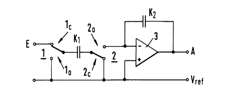
Figure la shows a circuit diagram of a simple SC cir-
cuit which can also be understood as the basic circuit
of extensive SC circuits on which the latter are built
up. An input E can, on the one hand, be connected via
a first switching path 1c of a first changeover switch
1 to a first terminal of a first capacitor K1 and, on
the other hand, can be connected via a second switch-
ing path to to a reference potential Vref, which may
be, for example, the potential of a circuit zero-
point.
A second terminal of the first capacitor K1 can be
connected, on the one hand, via a first switching path
20 of a second changeover switch 2 to an inverting in-
put of an operational amplifier 3 and, on the other
hand, can be connected via a second switching path 2c
CA 02216725 1997-09-29
8
to the reference potential Vref~ A non-inverting input ,
of the operational amplifier 3 is connected to the
reference potential Vref~ An output A of the oper-
ational amplifier 3 is connected via a second capac-
itor K2 to its inverting input and can consequently
also be connected to the second terminal of the first
capacitor K1.
In the switch position of the two changeover switches
1, 2 which is shown in Figure 1a, the first capacitor
K1 is charged by a signal present at the input E. If
the two changeover switches 1, 2 are brought to their
other switch positions, the charging is interrupted or
terminated and the charge which has passed to the
first capacitor K1 is forwarded to the second capac-
itor K2.
CMOS transmission gates can serve as an example of a
preferred realization of conducting and non-conducting
switching paths of changeover switches of SC circuits,
which CMOS transmission gates are, as is known, part-
ial circuits of integrated CMOS circuits, that is to
say of integrated circuits having complementary en-
hancement-mode insulated-gate field-effect transis-
tors. However, field-effect transistors of a uniform
conduction type can also be used to realize the
switching paths.
Figures ib and is show the realization of an open and
closed switching path So and Sc, respectively, by
means of a CMOS transmission gate. This comprises the
parallel circuit formed by the controlled current
paths of a P-channel transistor Tp and an N-channel
transistor Tn.
CA 02216725 1997-09-29
9
In order that, in accordance with Figure lb, both
transistors are switched off and consequently both
current paths are non-conducting, as is known a volt-
age VpD is present at the gate of the P-channel trans-
istor Tp and, at the same time, a voltage VSS is pre-
sent at the gate of the N-channel transistor Tn. The
voltage VDD is significantly more negative than the
gate threshold voltage of the P-channel transistor Tp,
and the voltage VSS is significantly more positive
than the gate threshold voltage of the N-channel
transistor Tn.
In order that, in accordance with Figure 1c, both cur-
rent paths of the two transistors are conducting, the
voltage VSS is now present at the gate of the P-chan-
nel transistor Tp and, at the same time, the voltage
VpD is present at the gate of the N-channel transistor
Tn. The voltage VpD is now significantly more positive
than the gate threshold voltage of the P-channel
transistor Tp, and the voltage VSS is significantly
more negative than the gate threshold voltage of the
P-channel transistor Tn. The two switched-on comple-
mentary transistors consequently realize a resistor
RAN, which can normally have a value of the order of
magnitude of 10 kn.
Figure 2 illustrates the basic circuit diagram of an
RC oscillator. Via an oscillator resistor W~, an os-
cillator changeover switch S~ switches an oscillator
capacitor KD back and forth between the voltages VpD
and VSS. In order that this proceeds in a free-running
manner, the junction point between the oscillator re-
sistor W~ and the oscillator capacitor K~ is connected
to an input of a Schmitt trigger 4, an output of which
is connected to the control input of the oscillator
CA 02216725 1997-09-29
changeover switch SO. A square-wave signal is thus
produced at this output, the frequency of which
square-wave signal is essentially determined by the
time constant of the RC element formed by the resistor
5 WO and the capacitor KO. As is known, this is equal to
the product of the value R of the resistor WO and the
value C of the capacitor KO.
Figure 3 shows a circuit diagram, which largely cor-
10 responds to the circuit diagram of Figure 2, of an RC
clock oscillator in accordance with one aspect of the
invention. The difference from Figure 2 consists in
the fact that the resistor WO is realized by a per-
manently switched-on CMOS transmission gate in accord-
ance with Figure 1c, with the result that the follow-
ing holds true for the value R of the resistor WO:
R ° RpN'
Figure 4 shows a basic circuit diagram of a customary
current-controlled clock oscillator which is realized
using CMOS technology. In this case, the resistor WO
according to Figures 2 and 3 is replaced by a CMOS
current mirror. The latter comprises a series circuit
formed by a P=channel resistor Pl and an N-channel
transistor N1 as well as a further P-channel trans-
istor P2 and a further N-channel transistor N2.
In the series circuit, the controlled current paths of
the P-channel transistor P1 and of the N-channel
transistor N1 are connected in series in such a way
that the drain of the P-channel transistor P1 is
connected to the voltage VpD and the source of the
N-channel transistor N1 is connected to the voltage
USS'
CA 02216725 1997-09-29
11
The drain of the P-channel transistor P2 is likewise
connected to the voltage VDp and the source of the
N-channel transistor N2 is likewise connected to the
voltage VSS. The gates of the two N-channel transist-
ors N1, N2 are connected to one another and, further-
more, are connected to the junction point between the
two transistors of the series circuit, that is to say
to the drain of the N-channel transistor N1 and to the
source of the P-channel transistor P1. The respective
gate of the two P-channel transistors P1, P2 is also
connected to this junction point.
The source of the further P-channel transistor P2 is
connected to a first input of the changeover switch SO
and the drain of the further N-channel transistor N2
is connected to a second input of the changeover
switch SO. The output of the latter is connected, as
in Figure 3, to the input of the Schmitt trigger 4 and
to the capacitor KO.
There is present between the voltage Vpp and the gate
of the P-channel transistor P1 a bias voltage Vb,
which codetermines the quiescent current IO flowing in
this transistor. The quiescent current IO can con-
sequently be set by the user by means of the bias
voltage Vb.
On account of the known properties of a current mir-
ror, this quiescent current IO thus also flows in the
further P-channel transistor P2 if, as is depicted in
Figure 4, the changeover switch SO is in the position
depicted, and consequently charges the capacitor KO.
When the Schmitt trigger 4 switches the changeover
switch SO to its other switch position, then the
capacitor KO is discharged again by the quiescent
CA 02216725 1997-09-29
12
current I~. This quiescent current I~ now flows,
namely, through the further N-channel transistor N2,
because this quiescent current also flows in the
N-channel transistor N1 and the current mirror
property dictates this.
Figure 5 shows a basic circuit diagram of a simple
differential amplifier, which is realized using P-
channel transistors, as the basic element of opera-
tional amplifiers. The differential amplifier com-
prises two amplifier transistors V1, V2, the drains of
which are connected to one another and are coupled to
the voltage VDD via the controlled quiescent current
path of a constant-current transistor V3. There is
present between the gate of the latter and the voltage
VDD a bias voltage Vbl, which codetermines the quiesc-
ent current Ib flowing in this transistor. Consequent-
ly, in this case, too, the quiescent current Ib can be
set by the user by means of the bias voltage Vbl.
A quiescent current I1 and, respectively, I2 flows in
the amplifier transistor V1 and in the amplifier tran-
sistor V2, in which case, as is characteristic of
differential amplifiers, the sum of these two currents
is constant and equal to the quiescent current Ib:
I1 + I2 = Ib = constant
The quiescent current Ib is divided between the two
amplifier transistors V1, V2 as a function of a
difference between variable signals vil and vi2
present at the respective gate of the amplifier
transistors V1, V2, with the result that variable
currents il, i2 flow in them. These currents il, i2
CA 02216725 1997-09-29
13
are further processed in further stages of the
operational amplifiers or in other stages of an
integrated circuit.
The following holds for the transconductance gm of
such a differential amplifier:
gm ° a(i1 - i2)/a(vil - vi2) ~ J2BpIbw/1.
In this, Bp is a production-dictated constant.
Despite various possible ways of realizing operational
amplifiers on the basis of the differential amplifier
basic element described, the transconductance of the
operational amplifiers is always a function of the
transconductance of the differential amplifier basic
element. Therefore, the bandwidth or the pole frequen-
cy fp of the operational amplifier is a function of
the quiescent current Ib, because the following holds
true for fp: fp = gm/(2~c), where the capacitive load
of the amplifier output is designated by c.
In the case of a two-stage amplifier, c is the known
Miller capacitance. At all events the capacitive load
c must be of the same type as the capacitors otherwise
used in the SC circuit and in the clock oscillator.
Figure 6 shows circuit diagrams of different simple
quiescent current setting circuits of MOS or CMOS
operational amplifiers. Figure 6a shows a P-channel
transistor P, the controlled current path of which is
connected in series with a resistor W between the
voltage VDD and the voltage VSS, which resistor has
the resistance R.
CA 02216725 1997-09-29
14
The gate of the transistor P is connected to its
junction point with the resistor W, and across this
gate is a bias voltage Vb1 codetermining the quiescent
current Ib which flows in the series circuit formed by
the resistor W and the transistor P. Codetermining
because the quiescent current Ib also depends on the
dimensioning of the channel of the transistor W, name-
ly on the quotient w/1 (w is the width of the said
channel and 1 is its length). The following holds true
for the quiescent current Ib:
Ib ~ (Vpp - Vgg - Vb1)/R.
In the circuit according to Figure 6b, the resistor W
of Figure 6a is replaced by a constant-current source
Q. In Figure 6c, the controlled current path of an
N-channel transistor N is connected in series with the
resistor W at the voltage Vss end. The gate of the
transistor N is connected to its junction point with
the resistor W, and across this gate is a bias voltage
Vb2, which additionally codetermines the quiescent
current Ib flowing in the series circuit formed by the
transistor P, the resistor W and the transistor N. The
following holds true here for the quiescent current
Ib:
Ib ~ (Vpp - Vgg - Vb1 - Vb2)/R.
In Figure 6d, the resistor W of Figure 6c is replaced
by a P-channel transistor DP connected as a diode, in
that the controlled current path of the said P-channel
transistor DP is inserted into the series circuit for-
med by the P-channel transistor P and the N-channel
transistor N. In this case, the gate of the transistor
CA 02216725 1997-09-29
Dp is connected to its junction point with the N-chan-
nel transistor N, that is to say also to the gate of
the latter.
5 In Figure 6e, the resistor W of Figure 6c is replaced
by an N-channel transistor DN connected as a diode, in
that the controlled current path of the said N-channel
transistor DN is inserted into the series circuit for-
med by the P-channel transistor P and the N-channel
10 transistor N. In this case, the gate of the transistor
DN is connected to its junction point with the P-chan-
nel transistor P, that is to say also to the gate con-
nection of the latter.
15 The respective transistor Dp or DN connected as a
diode usually has a small w/1 ratio, in order to
obtain a quiescent current setting circuit having a
small power loss.
Figure 6f shows a quiescent current setting circuit
having a very much smaller power loss. Two parallel
circuit paths are formed. The quiescent current Ib
flows in each of them. A first circuit path, the left-
hand one in Figure 6f, comprises, viewed starting from
the voltage VDD, the series circuit formed by the
P-channel transistbr P, the N-channel transistor N and
the resistor W. A second circuit path, the right-hand
one in Figure 6f, comprises, viewed starting from the
voltage VDD, the series circuit formed by a further P-
channel transistor P' and a further N-channel trans-
istor N'.
The gate of the further P-channel transistor P' is
connected to the gate of the P-channel transistor P.
The gate of the further N-Chazinei transistor N' is
connected to the gate of the N-cannel transistor N
CA 02216725 1997-09-29
16
and is connected to the junction point between the two
further transistors. The connection between the gate
of the N-channel transistor N and its drain, as is
present in Figure 6e, is not present.
The N-channel transistor has an increased w/1 ratio in
comparison with the respective w/1 ratio of these
transistors P, P', N'; this is illustrated by the de-
signation lx in the case of the transistors P, P', N'
and the designation 4x in the case of the transistor
N, where 4x is intended to indicate that the w/1 ratio
of the said transistor N is four times greater than
that of the transistors P, P', N'.
The current mirror formed by the transistors P, P'
ensures that the quiescent current Ib in the first
circuit path is identical to the quiescent current Ib
in the second circuit path. The gate-source voltage
VgsN. of the transistor N' is therefore smaller than
the gate-source voltage VgsN of the transistor N.
Consequently, the following holds true for the
quiescent current Ib:
Ib - ~VgsN' - VgsN)/R.
Figures 7a to 7c illustrate quiescent current setting
circuits comparable to Figures 6a, 6c and 6f, in which
circuits, according to the invention, the respective
resistor W is replaced by a permanently switched-on
CMOS transmission gate according to Figure 1c.
In order to illustrate the advantages which can be
achieved with the invention, the respective two par-
36 tial figures a) and b) of Figures 8 to 11 illustrate a
number of bar diagrams of the margin, the latter in
.' CA 02216725 1997-09-29
17
the sense defined above, cf. section g). The partial
figures a) each relate to the necessary settling time
of the MOS-SC circuit and the respective partial fig-
ures b) to the period of the clock signal.
In this case, the rectangles which are not filled in
represent the respective average tolerance ranges, the
hatched rectangles represent partial tolerance ranges
which are correlated with one another, and the narrow
filled-in rectangles represent typical values.
Figures 8a and 8b show, as was already mentioned
above, the average tolerance range of the requir-
ed settling time of an integrated MOS operational
amplifier (~ 50%) and, respectively, the toleran-
ce range of a crystal oscillator serv-ing as a
clock pulse generator. The resultant margin MQ in
this case amounts to approximately 55%.
Figures 9a and 9b show the conditions given with
an integrated MOS operational amplifier (toleran-
ce range again ~ 50%) and, respectively, a cus-
tomary on-chip RC oscillator as clock pulse gene-
rator, when there is no correlation between their
tolerance ranges. Figure 9a is identical to Fig-
ure 8a, and Figure 9b shows the average tolerance
range of the on-chip RC oscillator to be ~ 30%.
The margin MRC in this case amounts to approxim-
ately 80%.
Figures l0a and 10b show the conditions given
with a customary on-chip RC oscillator as clock
pulse generator when there is typical correlation
between their tolerance ranges. Figure l0a shows
the average tolerance range of the required
' CA 02216725 1997-09-29
18
settling time of an integrated MOS operational
amplifier of again ~ 50 % with a partial toleran-
ce range of ~ 25~.
Therefore, in Figure 10b, the left-hand edge of
the tolerance range of the on-chip RC oscillator
can be shifted to the typical value of Figure
10a. Since this tolerance range has a correlated
partial tolerance range likewise of ~ 25%, the
margin MRCk in this case amounts to only ~ 30%,
but this is still too large.
According to the invention, in accordance with
Figures ila and lib, it is now possible to in-
crease the respective partial tolerance range of
the settling time of the operational amplifiers
(Figure 11a) and of the on-chip RC oscillator
(Figure 11b) to in each case ~ 40%, with the
result that the margin MErf is now only ~ 10%.
Consequently, the design of the MOS-SC circuit
can be based on significantly improved boundary
conditions.
Although the conditions when using an on-chip RC
oscillator were explained with reference to Fig-
ures 8 to 11, comparable considerations also ap-
ply to the current-controlled oscillator accord-
ing to'the invention.
In cases where the tolerance of the power loss
cannot remain unconsidered, it is possible to
provide a trimmable and thus adjustable quiescent
current in the design of the layout of the MOS-SC
circuit. In that case, the total quiescent cur-
rent is increased when the resistance which de-
termines the quiescent current is increased. This
y ~ CA 02216725 1997-09-29
19
can be realized, for example, by connecting more
and more CMOS transmission gates in series or,
for example, by increasing the respective current
ratio of the current mirrors for the quiescent
current.
The setting value required for an individual
MOS-SC circuit can be determined in the course of
production during testing of the said circuit and
be stored in a memory, for example an EEPROM or
the like.
This quiescent current trimming does not increase the
margin MErf very much. A trimming margin of 25% norm-
ally suffices to achieve an acceptable supply current
tolerance, since the rise in the settling time error
of the switches on account of its exponential depend-
ence is not so large. Consequently, in the case of the
invention, the settling time error is less dependent
on supply voltage, temperature and process parameter
changes.