Language selection

Search

Patent 2216759 Summary

Third-party information liability

Some of the information on this Web page has been provided by external sources. The Government of Canada is not responsible for the accuracy, reliability or currency of the information supplied by external sources. Users wishing to rely upon this information should consult directly with the source of the information. Content provided by external sources is not subject to official languages, privacy and accessibility requirements.

Claims and Abstract availability

Any discrepancies in the text and image of the Claims and Abstract are due to differing posting times. Text of the Claims and Abstract are posted:

  • At the time the application is open to public inspection;
  • At the time of issue of the patent (grant).
(12) Patent Application: (11) CA 2216759
(54) English Title: OPTOELECTRONIC COMPONENT
(54) French Title: COMPOSANT OPTOELECTRONIQUE
Status: Dead
Bibliographic Data
(51) International Patent Classification (IPC):
  • G02B 6/36 (2006.01)
  • G02B 6/42 (2006.01)
  • H01R 9/00 (2006.01)
(72) Inventors :
  • GOTH, ALWIN (Germany)
  • ADAM, KLAUS (Germany)
  • REHM, WERNER (Germany)
  • FLORJANCIC, MATJAZ (Germany)
(73) Owners :
  • ALCATEL (France)
(71) Applicants :
  • ALCATEL ALSTHOM COMPAGNIE GENERALE D'ELECTRICITE (France)
(74) Agent: ROBIC
(74) Associate agent:
(45) Issued:
(22) Filed Date: 1997-10-16
(41) Open to Public Inspection: 1998-04-18
Examination requested: 2001-05-01
Availability of licence: N/A
(25) Language of filing: English

Patent Cooperation Treaty (PCT): No

(30) Application Priority Data:
Application No. Country/Territory Date
196 43 072.0 Germany 1996-10-18

Abstracts

English Abstract


An optoelectronic module is proposed which can be
coupled both optically and electrically in a simple
manner. It consists of an SMD package for the
electrical connection and a socket mating with an MT
plug for the optical connection. The SMD package is
adapted to the MT plug. It contains a socket which
contains the optical/electrical interface and which is
positively fixed in the package.


French Abstract

L'invention est un module optoélectronique qui peut être couplé optiquement et électriquement de façon simple. Il est constitué d'un boîtier de montage en surface pour la connexion électrique, ainsi que d'une prise de fiche MT pour la connexion optique. Ce boîtier est adapté à la fiche en question. Il contient une prise fixée solidement dans laquelle se trouve l'interface optique-électrique.

Claims

Note: Claims are shown in the official language in which they were submitted.


- 1 -

Claims

1. An optoelectronic component having at least one
electrical connection and at least one optical
connection, c h a r a c t e r i z e d i n that
the at least one electrical connection is formed by
external contacts (2) on an SMD package (1), and that
the at least one optical connection is formed by a
socket (5) which is compatible with an MT plug.

2. An optoelectronic component as claimed in claim 1,
characterized in that the external contacts (2) are
implemented in SO technology (SO = small outline).

3. An optoelectronic component as claimed in claim 1,
characterized in that the external contacts (2) are
implemented in BGA technology (BGA = ball grid array).

4. An optoelectronic component as claimed in claim 1
and in claim 2 or 3,
characterized in that the socket (5) is a molded part
which is positively and/or nonpositively fixed in the
package (1).


- 2 -


5. An optoelectronic component as claimed in claim 4,
characterized in that the socket (5) contains a
substrate (8) which supports optoelectronic converters
and/or passive optical components.

6. An optoelectronic component as claimed in claim 5,
characterized in that the socket connector (5) is
provided with a recess (9) containing the substrate
(8), which comprises an optoelectronic interface.

7. An optoelectronic component as claimed in claim 6,
characterized in that the optoelectronic interface
consists of at least one optical fiber (6) coupled to
an optical component (7).

8. An optoelectronic component as claimed in claim 7,
characterized in that the end of the optical fiber (6)
remote from the coupling point is contained in a bore
(11) provided in the molded part (10) between the
recess (9) and an end face of the molded part (10).

9. An optoelectronic component as claimed in claim 8,
characterized in that the package (1) contains a
printed circuit board (3) which supports the
electronic circuit required to operate the optical
component (7).

Description

Note: Descriptions are shown in the official language in which they were submitted.


CA 022167~9 1997-10-16


Optoelectronic Component

This invention relates to an optoelectronic component
having at least one electrical connection and at least
one optical connection.

Such components are increasingly needed in large
numbers in optical communications systems.
Accordingly, the technical problem to be solved by the
invention is to design such an optoelectronic
component in such a way that it can be manu~actured
and assembled e~ficiently and at low cost.

According to the invention, this technical problem is
solved by forming the at least one electrical
connection by means o~ external contacts on an SMD
package and the at least one optical connection by
means o~ a socket which is compatible with an MT plug.

Such an optoelectronic component can be manu~actured
at low cost and is easy to assemble.

Advantageous details of the invention are recited in
claims 2 to 9.

The invention will be now explained in more detail
with re~erence to the accompanying drawings, in which:

Fig. 1 shows a top view o~ an embodiment o~ the
optoelectronic component according to the
invention;

CA 022167~9 1997-10-16


Fig. 2 shows a longitudinal section of the
component o~ Fig. 1;

Fig. 3 shows details of the component in a
perspective view;

Fig. 4 shows a longitudinal section of the
socket; and

Fig. 5 shows a top view of the socket.

In the embodiment shown in Fig. 1, the optoelectronic
component is assumed to include an optoelectronic
interface, i.e., the component can be coupled to an
optical fiber whose optical signals are converted in
the component to electric signals.

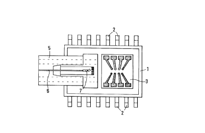
As can be seen in Fig. 1, the component has a housing
1 which is provided with external contacts 2. The
housing shown is implemented in SMD technology, i.e.,
it can be placed on a plane printed-circuit board and
the external contacts 2 can be soldered to conductive
tracks on the printed-circuit board. Connected to the
ends (not shown in Fig. 1) of the external contacts 2
which project into the housing 1 is a printed-circuit
board 3 which contains an electronic circuit 4 (Fig.
2) necessary for the operation of the optical
component.

Part of the inner ends of the external contacts 2 may
also be connected to a thermally highly conductive
plate or the like and serve to transfer the heat away
from a device disposed above the plate.

CA 022167~9 1997-10-16
. ~


Fixed in the housing 1 is a socket 5 which contains
the end portion of an optical fiber 6. The socket 5 is
the mate of an MT plug. MT plugs are known. They are
offered, for example, by EUROPTICS Ltd., Whiston,
Merseyside L35 IRZ, England. MT plugs are designed to
couple at least one optical fiber to another device
which also contains an optical fiber. To this end, the
optical fiber is fixed in a bore of the MT plug in
such a way that its end is flush with the external
surface of the MT plug. For precise alignment of the
MT plug, the latter has two guide pins at the external
surface at which the optical fiber ends.

The optical fiber 6 terminates at an optical component
7, e.g., a laser diode, in which the optical signal
transmitted by the optical fiber is converted to an
electric signal.

In Fig. 2, parts identical to parts shown in Fig. 1
are designated by like reference numerals. It can be
seen that the plug 5 has a substrate 8 fixed therein
on which the end portion of the optical fiber 6 is
held in place and which supports the optical component
7 as well as the electrical components necessary for
the operation of the optical component.

In Fig. 3, the substrate 8 with the optical component
7 disposed thereon and the optical fiber 6 coupled to
the optical component is shown in greater detail. The
optical fiber 6 is firmly confined in the substrate 8
in a V-groove, for example. The substrate 8 is
inserted into and fixed in a recess 9 in the socket 5
such that the free end of the optical fiber 6 lies in
a bore 11 extending from the recess 9 to the end face

CA 022167~9 1997-10-16


-- 4


10 of the socket 5, and that the end is flush with the
end face 10. Further bores 12 ending at the end face
10 of the socket 5 serve to receive the guide pins of
the MT plug.

The end of the socket 5 remote from the end face 10 is
provided, at the sides and below, with steps 13
corresponding to recesses 14 in the housing 1. These
serve to positively fix the socket 5 in the housing 1.
The socket 5 may additionally be bonded to the housing
1. It is also possible to only bond the socket 5 to
the housing.

Figs. 4 and 5 show details of the socket 5. They show
the shape of the recess 9 in which the substrate 8 is
fixed. A step 15 is provided for limiting the
longitudinal motion of the substrate 8. The bore 11
for receiving the optical fiber and the shape of the
step 13 are also clearly visible.

Representative Drawing
A single figure which represents the drawing illustrating the invention.
Administrative Status

For a clearer understanding of the status of the application/patent presented on this page, the site Disclaimer , as well as the definitions for Patent , Administrative Status , Maintenance Fee  and Payment History  should be consulted.

Administrative Status

Title Date
Forecasted Issue Date Unavailable
(22) Filed 1997-10-16
(41) Open to Public Inspection 1998-04-18
Examination Requested 2001-05-01
Dead Application 2003-10-16

Abandonment History

Abandonment Date Reason Reinstatement Date
2002-10-16 FAILURE TO PAY APPLICATION MAINTENANCE FEE

Payment History

Fee Type Anniversary Year Due Date Amount Paid Paid Date
Registration of a document - section 124 $100.00 1997-10-16
Application Fee $300.00 1997-10-16
Registration of a document - section 124 $50.00 1999-03-03
Maintenance Fee - Application - New Act 2 1999-10-18 $100.00 1999-09-28
Maintenance Fee - Application - New Act 3 2000-10-16 $100.00 2000-09-22
Request for Examination $400.00 2001-05-01
Maintenance Fee - Application - New Act 4 2001-10-16 $100.00 2001-09-18
Owners on Record

Note: Records showing the ownership history in alphabetical order.

Current Owners on Record
ALCATEL
Past Owners on Record
ADAM, KLAUS
ALCATEL ALSTHOM COMPAGNIE GENERALE D'ELECTRICITE
FLORJANCIC, MATJAZ
GOTH, ALWIN
REHM, WERNER
Past Owners that do not appear in the "Owners on Record" listing will appear in other documentation within the application.
Documents

To view selected files, please enter reCAPTCHA code :


To view images, click a link in the Document Description column. To download the documents, select one or more checkboxes in the first column and then click the "Download Selected in PDF format (Zip Archive)" or the "Download Selected as Single PDF" button.

List of published and non-published patent-specific documents on the CPD .

If you have any difficulty accessing content, you can call the Client Service Centre at 1-866-997-1936 or send them an e-mail at CIPO Client Service Centre.


Document
Description 
Date
(yyyy-mm-dd) 
Number of pages   Size of Image (KB) 
Drawings 1997-10-16 3 45
Cover Page 1998-09-14 1 36
Description 1997-10-16 4 125
Representative Drawing 1998-09-14 1 7
Claims 1997-10-16 2 52
Abstract 1997-10-16 1 13
Assignment 1999-03-03 13 377
Assignment 1997-10-16 4 132
Assignment 1999-05-26 11 211
Prosecution-Amendment 2001-05-01 1 30