Note: Descriptions are shown in the official language in which they were submitted.
CA 02216900 2001-02-15
7
METHOD TO EXTRACT CIRCUIT INFORMATION
This invention relates to the field of semiconductor integrated circuit
structure analysis.
BACKGROUND OF THE INVENTION
In the intensely competitive field of microelectronics, detailed analysis of a
semiconductor integrated circuit product can provide valuable information as
to how a particular
technical problem was dealt with, overall strengths and weaknesses of a design
approach, etc.
This information can be used to make decisions regarding market positioning,
future designs and
new product development. The information resulting from analysis of the
product is typically
provided through circuit extraction {reverse engineering), functional analysis
and other technical
means. At the core of this activity is the process of design analysis which.
in this context, refers
to the techniques and methodology of deriving complete or partial schematics,
starting with
essentially any type of integrated circuit in any process technology. For such
technical
information to be of strategic value it must be accurate and cost-effective,
and it is very important
that the information should be timely..
A design analysis process typically involves skilled engineers manually
extracting circuit
information from a set of large "photomosaics" of an integrated circuit (IC).
Skilled technicians
and engineers perform the following sequential manual tasks:
( 1 ) Capture Image:
(i) a high magnification photograph is taken, using a camera, of a small
portion of an IC
which has been processed to expose a layer of interest.
(2) step (i) is repeated for all of various regions of interest of the layer
of the IC, ensuring that
CA 02216900 1997-09-26
3
sufficient overlap exists between adjacent photographs that will be used to
create
photomosaics.
(3) Create Photomosaics:
(ii) all adjacent photographs associated with the given IC layer are aligned
and taped
together.
(4) steps (1)-(3) are repeated for all layers (1)-(N) necessary to construct a
complete visual
representation of the IC layers. All layers include interconnect layers. For
example, four
sets of photomosaics are required for a state-of the-art microprocessor
employing four
layers of interconnect: three layers of metal and one layer of polysilicon.
(5) Extract Circuit:
(iii) transistors, logic gates and other elements employed in the IC are
identified by
manually visually examining the polysilicon and lower metal interconnect
photomosaics.
(iv) interconnections between circuit elements of (iii) are traced and this
information is
captured in the form of schematic drawings.
(v) drawings of (iv) are manually checked against the photomosaics and any
obvious
errors are corrected.
(6) Organize Schematic:
(vi) the drawings of (v) are organized into hierarchial functional/logical
blocks.
(7) Capture Schematic:
(vii) the drawings of (vi) are entered into a computer using computer aided
engineering
(CAE) software tools for subsequent simulation and functional analysis of the
IC.
The aforenoted manual process used today has major limitations. The
photomosaics
alone for devices of current complexity are very expensive and can take many
months to create.
The circuit extraction task is labour intensive, tedious and error-prone. As
IC device geometrics
shrink toward 0.1 micron and levels of integration move toward the equivalent
of 1 billion
transistors on a single device, the current manual process for full-chip
design analysis will
become impractical.
CA 02216900 2001-02-15
4
In order to overcome the above-described manual process, automated systems
have been
designed. Such systems are described in U.S. Patent x,086,477 issued February
4th, 1992 to
Kenneth K Yu et al and U.S. Patent 5,191,213 issued March 2nd, 1993 to Haroon
Ahmed et al.
and also US Patent 5,694,481 issued December 2, 1997 to Lam et al.
In the system described in U. S. 5,086,477, the integrated circuit chip is
scanned by a
microscope or scanning electron microscope (SEM). The system identifies every
unique cell
and/or gate used in the integrated circuit. A unique abstract representation
is created for each of
these unique cells or gates, which are stored in a library.
However, without any operator guidance, the system cannot know where the
boundary of
a cell lies. While the patent suggests the use of diffusion edges to define
cell boundaries, it
appears that the only way that this can be done is by manual operator
direction.
In the patented system, once all unique cells have been captured in a
reference library, the
system attempts to associate and match all abstract features contained in the
layout data base to
the cells in the reference library using classical template matching. However
because of the
magnitude of data contained in a layout data base for a typical modern
integrated circuit, even
after the data has been compressed, the processing time required to reliably
extract a netlist is
large. The difficulty and time required for the operator directed process
becomes very difficult
with a large number of cells or gates, since the number of template matching
operations increases
exponentially with the number of reference cells and/or gates.
Once all reference cells in the patented system have been template matched to
the data
base, theoretically all features in the layout data base will have been
grouped and classified and a
netlist can be constructed. If all the futures of the layout data base have
been classified then a
netlist can be constructed. If there are features of the layout data base that
have not been
classified, either the system must construct a new cell or gate to be added to
the reference library
and an operator is informed, or the operator is informed by the system and the
operator performs
CA 02216900 2001-02-15
S
this task. The cell to cell interconnect information extraction, which is
required to construct a
netlist, is said to be performed using 'template matching, which is very
inefficient.
Due to the template matching approach that is required, the patented system
should be
limited to gate-array or very structured standard cell integrated circuit
analysis in which the large
majority of the cells are identical, since as the number of cells in the
integrated circuits increase.
the efficiency decreases. It is therefore inefficient for analysis of modern
ASICs or custom
integrated circuits, large and/or complex integrated circuits. The patented
system would also be
limited to applications where many devices from a few ASIC manufacturers are
investigated. due
to the investment and time required to develop separate reference libraries,
e.g. related to a
different set of design rules.
U.S. Patent 5,191,213 relates to a technique for removing layers of an
integrated circuit
and for scanning each of the layers.
1 ~ US Patent 5,694,481 to Lam et al discloses a system which performs the
following
steps, in the following order: a) image capture; b) image segmentation and
polygon generation; c)
registering (of polygon data); d) vertical alignment; e) schematic generation.
Although an
improvement over the prior art this technique still has its limitations, some
of them being:
1. Segmentation and polygon generation results are degraded around the
boundaries of each
of the images, which increased the amount of operator interaction. This could
be
minimized, by decreasing the perimeter to area ratio of the size of each image
being
captured. This minimizes the problem without solving the source.
2. Registering of polygon data is not as precise as registering of images.
Although a saving
is generated in terms of computing time, operator time, especially at the
vertical
alignment phase, is increased..
3. Vertical alignment employes a potentially large search to align the
different IC layers to
each other. This search involves aligning sets of contacts and vias to each
other from
successive layers. This task could be hampered by a number of reasons:
CA 02216900 1997-09-26
6
i. If deprocessing was poor, contacts/vias would not necessarily be easily
replicated from
layer-to-layer. Contacts/vias from successive layers may not necessarily be
available.
ii. The preferred embodiment of that invention used an SEM to perform image
capture.
Any SEM magnification drift could not be accommodated in the previous
disclosure.
iii. The search for a match could potentially be quite time consuming since no
previous
knowledge of a cross-reference point was available. Additionally, due to the
often
repetitive nature of integrated circuits, there was a chance of aligning the
layers at the
wrong location. If the ' layer misalignment' threshold was set too low, no
match may be
found.
4. No facility for correcting 'beam twist' in an SEM-like system is provided.
None of the previous techniques has the structure and advantages of the method
included
in the present invention.
SUMMARY OF THE INVENTION
The present invention overcomes the shortcomings of the above-described prior
art
manual design analysis process and the systems and processes described in the
aforenoted patents
by automating the entire process, including image capture, registration,
circuit readback, circuit
organization and schematic capture tasks. It should be understood that the
entire process is not
automated but rather that each portion has automation incorporated into it.
For example, the
operator will setup the parameters for capturing the images, and an operator
may also be required
to correct errors that are introduced by the circuit readback. Automation
presents many problems
which are solved by the present invention. The present invention can provide a
complete
analysis of an integrated circuit design in days or weeks (depending on the
size of the integrated
circuit), rather than the much greater time required in the prior art
processes, and months in the
case of the manual process.
CA 02216900 2001-02-15
The present invention relates t~o an automated system for extracting IC layout
information
using the following steps and criteria:
i. image capture of a highly magnified area of one layer from an integrated
circuit;
ii. computer controlled stage movement to allow the capture of a subsequent
image from the
integrated circuit. This image has overlap with previous images in the data
set. The stage
movement is either highly accurate (accurate being defined as having such a
small imprecision in
the measurement that the measurement can be treated as exact, or very near
exact), or returns a
precise stage location;
iii. the image magnification and/or fie:Id-of view are calculated from a
registration of two images
captured from (i) and (ii);
iv. the distortion from the beam twist is calculated from the registration
results between (i) and
(ii) which allows for compensation oi'."magnetic drift effects, including
magnification drift and
beam twist;
v. the results of (iii) are used to calculate the precise stage movements for
subsequent captures
(repeating {i) and (ii) until the entire set from the layer has been captured;
vi. a fiducial mark (local landmark) is imaged which will be common for all
the IC layers. The
relative position between this fiducial mark and the start of data set is
calculated;
vii. optionally, statistical information. can be gathered and used to verify
and/or reject a
registration result;
viii. after registering has been completed for all edges of an image, polygons
can be generated
from that image using the registered data set;
ix. repeat steps (i)-(viii) for all IC layers;
x. vertically align the layer datasets with each other using the results of
(vi);
xi. generate a netlist and optionally a. schematic using the results of (x).
The present invention is an improvement over US Patent 5,694,481 to Lam et al
thxough the following modifications,
i. registration (mosaicking) of the images is performed using the image
(pixel) data rather than
the polygon data. This increases the registration accuracy and reduces
operator intervention,
CA 02216900 2001-02-15
g
especially at the vertical registration step;
ii. registering is performed either prior to segmentation and polygon
generation or pipelined with
segmentation and polygon generation, rather than after. Additionally, images
with no features
can be more easily registered than in US Patent x,694,481 to Lam et al;
iii. segmentation and polygon generation results are improved by using the
registered image data,
rather than the individual images as the input to these tasks. This
effectively eliminates the
image boundaries and eliminates all inaccurate polygons which would be created
due to the
discontinuities at the image boundaries;
iv. a highly accurate stage- either a position measurement system, or
physically accurate- (with
I 0 precision at least one order of magnitude greater than the minimum feature
size being imaged) is
used.
This allows for the following improvements:
1 ~ (a) the search window for registering can be reduced since the relative
positions of the images are
known, instead of known within the precision of the stage, where this position
was potentially
either greater, or on the order of the nninimum feature size. This reduces
redundant data and
reduces processing time by two order's of magnitude;
(b) after one registering operation has been performed, the magnification and
the field-of view of
20 each image is known. This allows for automatic scaling of the images if
required due to drift of
the SEM effective magnification;
(c) image distortion due to "beam twist" can be precisely corrected for;
(d) with the addition of a local landrr~ark on the IC layer being imaged, the
vertical registration
technique presented in US Patent S,fi94,481 does not need to be used. Instead,
the positions read
25 from the positioning system can be used to perform the vertical alignment;
(e) additionally, with the addition of the "local landmark", mutual-rotation
between the layer-sets
can be corrected since a highly accurate stage is used.
CA 02216900 2001-02-15
9
In accordance with another object of the present invention there is provided a
method of
analyzing at least a portion of an integrated circuit (IC) comprising the
steps of: (a) scanning at
feast a portion of a layer of an IC using high magnification, to obtain stored
images of said
portion of the IC; (b) registering the stored images; (c) creating a layout
database from the stored
images in the form of a set of polygons representing the IC layout of at least
some of the layers;
(d) repeating steps (a), (b) and (c) for plural layers of the IC; (e)
registering the sets of polygons
from each layer into alignment with minimal distortion; and (f) generating a
netlist and/or
schematic diagram of circuitry represented by at least a portion of the IC
from the aligned
registered sets of polygons.
In accordance with yet another object of the present invention there is
provided a method
of analyzing at least a portion of an integrated circuit (IC} comprising the
steps of: (a) scanning at
least a portion of a layer of an IC using high magnification, to obtain stored
images of said
portion of the IC; (b) registering the stored images; (c) creating a layout
database from the stored
1 ~ images in the form of a set of polygons representing the IC layout of at
least some of the layers;
(d) repeating steps (a), (b) and (c) for. plural layers of the IC; (e)
registering the sets of polygons
from each layer into alignment with minimal distortion.
Further objects and advantages of the present invention will be apparent from
the
following description, wherein preferred embodiments of the invention are
clearly shown.
BRIEF DESCRIPTION OF THE DRAWIiVGS
A better understanding of the invention will be obtained by reading the
description of the
invention below, with reference to the following drawings, in which:
Figure lA illustrates multiple IC layers and a SEM device; and
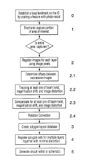
Figure 1B is a flow chart generally illustrating the present invention.
CA 02216900 1997-09-26
DETAILED DESCRIPTION OF THE INVENTION
The corresponding steps performed by the system are shown in the flow chart of
Figure 1.
The system is comprised of an image acquisition apparatus 1 for acquiring
electronic high
5 magnification image sets of an IC. Once the entire area of interest has been
captured, registering
2 of the images, representing each layer, is performed. The creation of
polygons 3 then takes
place prior to registering all layers 4 together. It should be noted that the
polygons do not
necessarily need to be created prior to registering all layers together.
Finally, a circuit netlist is
generated 5.
Registering is performed in the pixel domain instead of the polygon domain
because
image capture and image registration require about the same computing
resources as polygon
generation. This provides several advantages:
i. Registering can be performed prior to segmentation, either in parallel or
pipelined with segmentation and polygon generation. This introduces a
performance enhancement.
ii. High-speed accelerator boards can be employed to perform the correlation
with
very little engineering effort (since off the shelf routines can be employed).
iii. Sub-pixel registering techniques can be employed. By performing a
registering of such high accuracy, little or no error is introduced into the
placements, even in very large data-sets (grids consisting of 10000 images or
more). Although this requires more computing resources, it in turn reduces the
operator interaction required, especially at the vertical alignment phase.
iv. Since registering is performed before or in a pipelined fashion with
segmentation/polygon generation, features at the boundary are verified by
bypassing the discontinuity introduced by the image boundary.
Pixel based registering, is in general a very compute-intensive task. The task
is sped up
by collecting statistical information such as the mean, variance, standard
deviation, integral,
CA 02216900 1997-09-26
11
skewness, kurtosis, entropy, contrast etc. These statistics can be calculated
very quickly. They
can be calculated for the window and the template at each location, as
required. Predefined
thresholds can be used to disable the calculation of a correlation when the
templated windows are
recognized as being statistically different.
The registering enhancement actually improves system performance by increasing
the
quality of the polygons generated (at the image boundaries) because the data
from the adjacent
images can be taken into consideration as well as improves the quality of the
registration, thus
allowing larger data-sets to be captured with less user interaction
Vertical alignment is improved by performing two operations. The first
operation is to
reduce the search window. By selecting some feature and masking it such that
subsequent
sample preparation (such as chemical etches, for example) cannot effect that
region, a suitable
'local landmark' exists which allows the data-sets from two separate devices
(i.e. metal 1 and
metal 2 layers) to be correlated to each other. A local landmark (fiducial
mark) can be any
feature which is visible on the top-level layer of interconnect, such as an
edge seal, a pad, or an
on-chip registration mark. These can be masked using standard techniques
(coating the feature
with photo-resist before etching the rest of the device). The global positions
of the fiducial
marks are known in the co-ordinate system of the stage. The global positions
of the start of the
data-sets from each layer are also known. By subtracting the global position
of the data-sets from
the global position of the fiducial mark from that layer (or vice-versa), the
local coordinates of
the data-sets are extracted. Within the precision of the stage, and position
measurement
apparatus, the relative positioning of the two data-sets are known. This can
be repeated for all
layers. Since the search window is actually quite small now, known procedures
can be used to
perform the alignment. Even a manual approach could be used.
The burden on sample preparation is also reduced using the techniques
described above.
Since alignment does not rely on the presence or-absence of contact/via
information, contacts and
vias need only appear on one of the layers to which they connect. Performing
sample preparation
CA 02216900 1997-09-26
12
such that contact/via information is reliably reproduced on two IC layers is a
significant burden.
Since the alignment has been performed, the classification can be performed
using a simple set of
rules based on metal/polysilicon/diffusion coverage of the contacts/vias.
Since the IC layer from
which the contacts/vias are captured from is known, the class of contact/via
has been reduced to
either one or two different possibilities. For example, a via captured on the
M2 layer of a 2 layer
metal process must be a via if it is surrounded by both M2 and M 1. If vias
are not imaged on M 1
(due to sample preparation), the contacts, imaged with M 1 must be polysilicon-
metal contacts (if
they are surrounded by metal 1 and polysilicon) or diffusion-metal contacts
(if they are
surrounded by metal 1 and diffusion). For a two metal, 1 polysilicon CMOS
process,
contacts/vias can be imaged in any of the following scenarios without any loss
of interconnection
information:
i. M2-none, M1-vias, Polysilicon/Diffusion-Contact
ii. M2-vias, M 1-none, Polysilicon/Diffusion-Contact
iii. M2-vias, M 1-Contact, Polysilicon/Diffusion-none
This table refers to the fact that for each main-interconnect being imaged
(i.e. layer M1,
M2 etc..) another layer is imaged (or not necessarily imaged) as well (i.e.
layer contact, or via).
Additionally, if contacts and/or vias can be imaged on multiple layers, the
number of
combinations increases even more. Rules are added to accommodate these cases,
such as
looking for repeated vias between M2 and M1 or repeated contacts between
diffusion/metal 1 or
polysilicon and metal 1. By increasing the permutations in which contacts/vias
can be imaged
from the devices, the burden on sample preparation is reduced, and the quality
of samples used
for processing are increased.
If a highly accurate (accurate being defined as having such a small
imprecision in the
measurement that the measurement can be treated as exact, or very near exact)
stage (or accurate
position measurement system) is used, then the burden on both registering and
vertical
CA 02216900 1997-09-26
13
registration is reduced For example, the stage may have optical encoders which
can measure the
position to +/- 1 micron. This is a large imprecision, for example, if the
minimum feature being
imaged is 0.3 microns. Using a laser interferometer, for example, to measure
the stage position,
the position can be determined to less than 0.05 microns of accuracy. In most
cases, this
precision is sufficient to just place adjacent images next to each other if
the magnification is
known. With standard SEM-type imaging systems, the magnification usually
cannot be
guaranteed to less than 5% accuracy. This potential deviation is large enough
that the field size
(in microns) of the captured image cannot be known to high enough accuracy.
The field size (or
magnification) can be known precisely by performing a registering step once in
the X direction
14 and once in the Y-direction or by imaging a known standard. Additionally,
if drift in the image
capture, scan electronics etc. are ignored, all subsequent images captured
from a single layer can
be placed in a registered set using the position read from the laser
interferometer without a
correlation step. Since the electronics do drift (in the case of the JEOL
5800, they drift, on
average, by 0.025 microns/minute), correlations will be required for at least
some images. The
interval between correlations depends on the size of the image set, the
magnification in which the
images are being captured, and the amount of time between successive image
captures.
By using the positioning system, a few advantages have been gained:
i. The number of correlations required have been significantly reduced since
they do not
necessarily need to be performed between every image pair. Additionally, the
search
window required for the correlation has been reduced in size, thus reducing
the
calculations at each step. Further, by tracking the drift in the electronics,
even the search
window at the start of the subsequent rows can be minimized.
ii. Imaging instruments like SEM's can display drifts in magnification when
the critical
parameters such as the working distance are varied. These drifts are difficult
to correct
manually. With either an accurate stage, or measurement system, these drifts
can be
easily calculated using the field of view extracted from the registering
(without the
positioning/measurement system the magnification can only be calculated to the
precision
CA 02216900 1997-09-26
14
of the stage and electronics). Once this value is calculated, polygon data can
be quickly
re-scaled using standard techniques.
Above, we justified the addition of a single fiducial mark common to all
devices to allow
the creation of a local-coordinate system which is common to all de-layered
samples. By placing
this fiducial mark at one end of the device to be imaged, and placing a second
fiducial mark at a
location widely separated from the first fiducial mark (ideally, as far away
as possible from the
first fiducial mark, or at least along the long axis of the IC), either the
mutual rotation between
different IC layers, or the rotation with respect to the stage or capture axes
can be calculated very
precisely (the baseline is very long with respect to the error in the position
measurements). This
angle can then be used to rotate the different image sets such that they have
no rotation with
respect to each other. By using a point at the center of each image, the
effects of beam twist on
the inaccuracy of these measurements can be minimized. Beam twist is caused by
the electrons
spiraling in the magnetic field of an SEM-like instrument. This twist can be
simply modeled, to a
first order, by a rotation of each image around the center point of the image.
By measuring the
angle of a straight line across a single image, and compensating for the
effective rotation, beam
twist can be calculated. This effective rotation can then be corrected on each
and every image
captured, since this angle will remain approximately constant (any tilt in the
device with respect
to the electron source will vary the angle slightly-but even this can be
compensated for, if
required, by using a measurement system to extract the tilt angle, and either
zero it, or
compensate for it using a scaled rotation correction). This rotation
correction is applied before
registering is performed. The rotation due to the stage image axes rotation
can be corrected at
any time after registering has been performed. Because of the precision of the
positioning system
of the invention, the offsets (or overlap) that are calculated between
successive images (which
are overlapped by a small amount) can be used to determine the magnification
at which the
image is captured and thereby track beam twist and any magnification drift
and/or image
distortion.
CA 02216900 1997-09-26
The invention may be embodied in other specific forms without departing from
the spirit
or essential characteristics thereof. The present embodiments are therefore to
be considered as
illustrative and not restrictive, the scope of the invention being indicated
by the appended claims
rather than by the foregoing description, and all changes that come within the
meaning and range
5 of equivalency of the claims are therefore intended to be embraced therein.