Language selection

Search

Patent 2216911 Summary

Third-party information liability

Some of the information on this Web page has been provided by external sources. The Government of Canada is not responsible for the accuracy, reliability or currency of the information supplied by external sources. Users wishing to rely upon this information should consult directly with the source of the information. Content provided by external sources is not subject to official languages, privacy and accessibility requirements.

Claims and Abstract availability

Any discrepancies in the text and image of the Claims and Abstract are due to differing posting times. Text of the Claims and Abstract are posted:

  • At the time the application is open to public inspection;
  • At the time of issue of the patent (grant).
(12) Patent: (11) CA 2216911
(54) English Title: DEFINING AN ELECTRODE AREA
(54) French Title: DEFINITION D'UNE ZONE D'ELECTRODE
Status: Deemed expired
Bibliographic Data
(51) International Patent Classification (IPC):
  • G01N 27/416 (2006.01)
  • B01D 67/00 (2006.01)
  • B29C 44/56 (2006.01)
  • G01N 27/30 (2006.01)
(72) Inventors :
  • HODGES, ALASTAIR MCINDOE (Australia)
  • BECK, THOMAS WILLIAM (Australia)
  • JOHANSEN, ODDVAR (Australia)
(73) Owners :
  • LIFESCAN, INC. (United States of America)
(71) Applicants :
  • MEMTEC AMERICA CORPORATION (United States of America)
(74) Agent: BULL, HOUSSER & TUPPER LLP
(74) Associate agent:
(45) Issued: 2006-06-06
(86) PCT Filing Date: 1996-04-11
(87) Open to Public Inspection: 1996-10-17
Examination requested: 2002-11-04
Availability of licence: N/A
(25) Language of filing: English

Patent Cooperation Treaty (PCT): Yes
(86) PCT Filing Number: PCT/AU1996/000210
(87) International Publication Number: WO1996/032635
(85) National Entry: 1997-09-25

(30) Application Priority Data:
Application No. Country/Territory Date
PN 2393 Australia 1995-04-12

Abstracts

English Abstract


The present invention relates to a method for defining an area (4) of a layer
on a porous substrate comprising compressing a volume
of the substrate to produce a compressed region (8) which defines, or which in
combination with an edge (7) of the substrate or of the layer
defines, a boundary of the area and which substantially prevents the transport
of material through or across its surface. The present invention
also relates to an electrochemical sensing device comprising: a porous
substrate; and an electrode (1) on one side of the substrate; wherein
a region of the substrate is compressed to an extent which forms a barrier to
migration of electrolyte within the substrate, the compressed
region defining, or in combination with an edge of the substrate or the
electrode defining, a zone on the electrode of predetermined area.


French Abstract

La présente invention concerne un procédé servant à définir une zone (4) d'une couche sur un substrat poreux, consistant à comprimer un volume du substrat pour produire une région comprimée (8) qui définit, seule ou en combinaison avec un bord (7) du substrat ou de la couche, une limite de zone et qui empêche sensiblement le transport de matériau à travers sa surface. La présente invention concerne également un détecteur électrochimique comprenant: un substrat poreux; et une électrode (1) sur un côté du substrat; dans lequel une région du substrat est comprimée à un degré permettant de faire obstacle à la migration d'électrolyte à l'intérieur du substrat, ladite région comprimée définissant, seule ou en combinaison avec un bord du substrat ou de l'électrode, une zone sur l'électrode d'une surface prédéterminée.

Claims

Note: Claims are shown in the official language in which they were submitted.


-13-

CLAIMS:

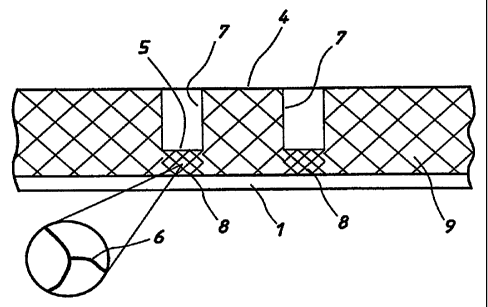
1. A method for defining an area of a layer on a porous substrate comprising
compressing a volume of the substrate to produce a compressed region which
defines,
or which in combination with an edge of the substrate or of the layer defines,
a
boundary of the area and which substantially prevents the transport of
material
through or across its surface.
2. A method according to claim 1, wherein the layer is either attached to or
in
contact with the porous substrate or is a coating applied to the substrate.
3. A method according to claim 1 or claim 2, wherein the layer is an electrode
and the area being defined is an electrode area.
4. A method according to claim 3, wherein the electrode is formed on the
surface of the substrate by a method selected from the group consisting of
electroless
plating, electroplating, evaporation, and sputtering.
5. A method according to claim 4, wherein the electrode is sputter deposited
on
the surface of the substrate to form a continuous film.
6. A method according to claim 5, wherein the film thickness on the substrate
is
to 200 nm.
7. A method according to claim 6, wherein the film thickness is 60 to 120 nm.
8. A method according to any one of claims 3 to 7, wherein the electrode is
made of materials selected from the group consisting of gold, silver,
platinum,
palladium, iridium, lead and alloys of those metals, carbon, carbon mixed with
a
binding material, and silver partially covered with a porous layer of an
insoluble silver
salt.


-14-

9. A method according to claim 8, wherein the insoluble silver salt is silver
chloride, silver bromide, silver iodide, silver ferrocyanide or silver
ferricyanide.
10. A method according to any one of claims 1 to 9, further including a
blocker
in the substrate which assists in preventing transport of material in the
compressed
region.
11. A method according to claim 10, wherein the blocker is glucose, agar,
gelatine or starch.
12. A method according to claim 10 or claim 11, wherein the blocker is loaded
into the precompressed porous substrate using the steps of:
a) dissolving the blocker in a suitable solvent;
b) wetting the substrate with the solution of the blocker; and then
c) removing the solvent by evaporation.
13. A method according to any one of claims 1 to 12, wherein the substrate is
made of a porous material selected from the group consisting of polymers or
mixtures
of polymers.
14. A method according to claim 13, wherein the polymers or mixtures of
polymers consist of polysulfones, polyvinylidene halides, tetrafluoroethene,
polyamides, polyimides, polyethylene, polypropylenes, polyacrylonitrides or
polycarbonates.
15. A method according to claim 14, wherein the polyvinylidene halides are
polyvinylidene difluorides.
16. A method according to any one of claims 1 to 15, wherein the thickness of
the precompressed substrate is about 180µm or less.


-15-

17. A method according to claim 16, wherein the thickness of the precompressed
substrate
is from 30µm to 150µm.
18. A method according to any one of claims 1 to 17, wherein the pore size of
the
substrate ranges from 10 kilodaltons cut-off(lower limit) to 5 microns.
19. A method according to claim 18, wherein the pore size of the substrate
ranges from 0.1
µm to 0.8 µm.
20. A method according to claim 19, wherein the pore size of the substrate
ranges
from 0.2 µm to 0.5 µm.
21. An electrochemical sensing device comprising:
a porous substrate; and
an electrode on one side of the substrate; wherein a region of the substrate
is
compressed to an extent which forms a barrier to migration of electrolyte
within the substrate,
the compressed region defining, or in combination with an edge of the
substrate or the
electrode defining, a zone on the electrode of predetermined area.
22. An electrochemical sensing device according to claim 21, wherein the
electrode is
formed on one side of the substrate by a method selected from the group
consisting of
electroless plating, electroplating, evaporation, and sputtering.
23. An electrochemical sensing device according to claim 22, wherein the
electrode is
sputter deposited on the surface of the substrate to form a continuous film.
24. An electrochemical sensing device according to claim 23, wherein the film
thickness
on the substrate is 10 to 200 nm.
25. An electrochemical sensing device according to claim 24, wherein the film
thickness
is 60 to 120 nm.


-16-

26. An electrochemical sensing device according to any one of claims 21 to 25,
wherein
the electrode is made of materials selected from the group consisting of gold,
silver, platinum,
palladium, iridium, lead and alloys of those materials, carbon, carbon mixed
with a binding
material, and silver partially covered with a porous layer of an insoluble
silver salt.
27. An electrochemical sensing device according to claim 26, wherein the
insoluble silver
salt is silver chloride, silver bromide, silver iodide, silver ferricyanide or
silver ferrocyanide.
28. An electrochemical sensing device according to any one of claims 21 to 27,
wherein
there are two or more electrodes and they are disposed on one side of the
substrate or on
opposite sides of the substrate.
29. An electrochemical sensing device according to any one of claims 21 to 28,
further
including a blocker in the substrate which assists in preventing transport of
material in the
compressed region.
30. An electrochemical sensing device according to claim 29, wherein the
blocker is
glucose, agar, gelatine or starch.
31 An electrochemical sensing device according to claim 29 or claim 30 wherein
the
blocker is loaded into the precompressed porous substrate using the steps of:
a. dissolving the blocker in a suitable solvent;
b. wetting the substrate with the solution of the blocker; and then
c. removing the solvent by evaporation.
32 An electrochemical sensing device according to any one of claims 21 to 31
wherein
the substrate is made of a porous material selected from the group consisting
of polymers or
mixtures of polymers.


-17-

33. An electrochemical sensing device according to claim 32, wherein the
polymers or
mixtures of polymers consist of polysulfones, polyvinylidene halides,
tetrafluoroethene,
polyamides, polyimides, polyethylene, polypropylene, polyacrylonitrates or
polycarbonates.
34. An electrochemical sensing device according to claim 33, wherein the
polyvinylidene
halides are polyvinylidene difluorides.
35. An electrochemical sensing device according to any one of claims 21 to 34,
wherein
the thickness of the precompressed substrate is about 180 µm or less.
36. An electrochemical sensing device according to claim 35, wherein the
thickness of the
precompressed substrate is from 30 µm to 150 µm.
37. An electrochemical sensing device according to any one of claims 21 to 36,
wherein
the pore size of the substrate ranges from 10 kilodaltons cut-off (lower
limit) to 5 microns.
38. An electrochemical sensing device according to claim 37, wherein the pore
size of the
substrate ranges from 0.1 µm to 0.8 µm.
39. An electrochemical sensing device according to claim 38, wherein the pore
size of the
substrate ranges from 0.2 µm to 0.5 µm.
40. An electrochemical sensing device according to any one of claims 21 to 39,
wherein
the porous substrate is a membrane that is permeable to a fluid containing a
first species to be
analysed but substantially impermeable to a second species contained in the
fluid, the second
species being of a kind which would interfere with the electrochemical sensing
of the first
species.

Description

Note: Descriptions are shown in the official language in which they were submitted.


CA 02216911 1997-09-25
WO 96/32635 PC'T/AU96/00210
DEFINING AN ELECTRODE AREA
TECIiNICAL FIELD:
The present invention relates to a method for defining an area of a coating or
layer attached to or in contact with a porous substrate. More particularly,
the present
invention relates to a method wherein the coating or layer is an electrode.
Although
the invention will be described with reference to its application in the
electrochemical
area it is not intended that the invention be limited to that use. It may
extend to any
application where a defined area of a porous substrate is required.
BACKGROUND ART:
1 o In the past it has been found that whenever quantitative electrochemical
measurements are performed it is necessary to have both a reproducible and
accurately
defined electrode area which is in contact with the sample being analysed.
When
performing a measurement in a bulk solution the usual practice has been either
to have
the electrode immersed to a certain level in the liquid or alternatively to
have an
insulation layer applied to the electrode to leave only a precisely defined
area in


CA 02216911 1997-09-25
WO 96/32635 PCT/AU96/00210
-2-
contact with the solution. These practices have proved to be relatively
expensive and
unreliable. It has also been found that when these methods are used it is
di~cult to
prevent leakage and contact with the electrode outside the defined area,
especially
when the substrate upon which the electrode is placed is porous.
The present invention seeks to overcome or at least ameliorate the problems of
the prior art by providing a method which is inexpensive, simple to apply and
reliable.
SUMMARY OF THE INVENTION:
According to one aspect the present invention consists in a method for
defining
an area of a layer on a porous substrate comprising compressing a volume of
the
substrate to produce a compressed region which defines, or which in
combination with
an edge of the substrate or of the layer defines, a boundary of the area and
which
substantially prevents the transport of material through or across its
surface.
According to a second aspect the invention consists in an electrochemical
sensing device comprising:
a porous substrate; and
an electrode on one side of the substrate; wherein a region of the
substrate is compressed to an extent which forms a barrier to migration of
electrolyte
within the substrate, the compressed region defining, or in combination with
an edge
of the substrate or the electrode defining, a zone on the electrode of
predetermined
area.
According to a third aspect the porous substrate of the second aspect is a
membrane that is permeable to a fluid containing a first species to be
analysed but
substantially impermeable to a second species contained in the fluid, the
second


CA 02216911 1997-09-25
R'O 96/32635 PCT/AU96/00210
-3-
species being of a kind which would interfere with electrochemical sensing of
the first
species.
Preferably, the layer, which may be attached to or in contact with the porous
substrate or may be a coating applied to the substrate, is an electrode and
the area
being defined is an electrode area. When the layer is an electrode it is
usually sputter
deposited on the surface of the substrate so as to form a continuous film on
the
surface. However, other methods such as electroless plating, electroplating,
evaporation, anodization or the like can be used to form the electrode.
Usually the
film thickness on the substrate is 10-200nm, more preferably 60-120nm.
l0 Materials which would be suitable as an electrode include gold, silver,
platinum, palladium, iridium, lead, and alloys of those metals, carbon, carbon
mixed
with a binding material, and silver partially covered with a porous layer of
an
insoluble silver salt such as silver chloride, silver bromide, silver iodide,
silver
ferricyanide and silver ferrocyanide. In electrochemical sensing devices
according to
the invention there will typically be two or more electrodes and these may be
disposed
on one side of the substrate or on opposite sides of the substrate.
In a preferred form the resulting substrate produced from the method of the
invention will have at least two discrete regions - one region being
compressed and the
other region being uncompressed. This resulting substrate has been found to be
2o particularly useful when used as an electrochemical sensing device. When a
sample is
placed on the uncompressed region of the resulting substrate, migration of the
sample
to another region of that substrate, being divided from the first region by
the
compressed region, is substantially prevented. It has been found that the
sample is


CA 02216911 2005-05-31
wo s rcrmie
-4-
confined to a ptedetamined area of the res~rltiag substrate aad therefore to a
pr~e~rtained area of the electrode attached to or otherwise in contact with
the
The method of the present invemion works by substantially eliminating or
s st~ciendy constricting the porous structure of the substrate in the
comprregion
to render that region egectively impermeable.
The method of the present invention can be used alone or preferably, in
c~junction with a blocker. A blocks, in tlx prat invention, is a sub~nCe which
is placed in the substrate such that it does not prevent the transport of
material in the
1o vmcompiregions of the substrate but assists in preventing transport of
material in
the compressed areas. Examples of material suitable as a blocky may include
glucose, agar, gelatine, starch or the like.
In a prefened form the blocker is conveniently loaded into the precompressed
porous substrate using the steps of
~s (a) dissolving the blocker in a suitable solvent;
(b) wetting the substrate with the solution of the blocker; and then
(c) removing the solvent by evaporation.
In another preferred form the pomus substrate is of a kind' having pores which
increase in diameter from a smooth or shiny side to a rough side. The porous
substrate
2o is desirably of the kind disclosed in U.S. Patent Nos 4,629,563 and
4,77,039 . However
according to end use the substrate may be an asymmetric or symmetric membrane.


CA 02216911 1997-09-25
WO 96132635 PCT/AU96/00210
-5-
The substrate may be any suitable porous material that is compressible and
which will maintain its mechanical integrity during compression. Examples of
such
materials include polymers or mixtures of polymers such as polysulfones,
polyvinylidene halides such as polyvinylidene diffuorides, tetrafluoroethene,
polyamides, polyimides, polyethylenes, polypropylenes, polyacrylonitrites,
polycarbonates or the like. The materials may be in the form of a sheet, tube
or
hollow fibre which have microscopic or macroscopic pores.
The thickness of the substrate is selected with the end use in mind. Usually
it
is desirable for the substrate to be thin to minimise sample volume. However,
to sufficient thickness is required to provide mechanical strength for
handling and to
maintain su~cient separation between electrodes on opposite faces of the
substrate to
prevent electrical short circuits.
In some applications for example anodic stripping, larger sample volumes and
greater thickness will be preferred. Preferred embodiments and illustrative
examples
of the present invention will now be described, by way of example only, with
reference to the accompanying figures, in which:-
BRIEF DESCRIPTION OF THE FIGURES:
Figure 1 shows a cross-sectional view of a microporous substrate in
uncompressed form, with a portion shown as an enlarged image;
Figure 2 shows the substrate of Figure 1 with compressed regions in
combination with the edge of the microporous substrate to define a perimeter
of the
area with a portion of the compressed region shown as an enlarged image;
Figure 3 shows a top view of the substrate of Figure 2;


CA 02216911 1997-09-25
WO 96/32635 PCT/AU96I00210
-6-
Figure 4 shows an end view of the substrate of Figures 1 or 2;
Figures 5 is similar view to Figure 1 where a blocker has been added to the
substrate;
Figure 6 is a similar view to Figure 2 where a blocker has been added to the
substrate;
Figures 7 is a top view of one embodiment differing in respect of defined
target areas;
Figure 8 is a top view of a second embodiment differing in respect of target
areas;
1 o Figure 9 is a top view of a third embodiment differing in respect of
target
areas;
Figure 10 is a top view of a fourth embodiment differing in respect of target
areas; and
Figure 11 shows a top view of a preferred embodiment of the invention.
Figure 1 illustrates a microporous substrate 10 in an uncompressed form
having an electrode 1 being attached to or in contact with substrate 10. The
thickness
of the precompressed substrate is preferably about 180pm, more preferably from
30-
150p,m. The pore size ranges from 10 kilodaltons cut-off (lower limit) to 5
microns
and preferably from O.lp.m to 0.8p,m, more preferably from 0.2p.m to 0.5~m.
Also
2o shown in Figure 1 is the magnified image which shows the uncompressed pores
2 of '
the substrate. When pressure is applied to an area 5 of the microporous
substrate 10,
one or more discrete compressed regions 8 are produced. As shown in Figure 2
and 3
the compressed regions 8 in combination with the edges 7 of the uncompressed
region


CA 02216911 1997-09-25
WO 96!32635 PCT/AU96100210
_7_
define a boundary of the area 4. This compressed region 8 substantially
prevents the
transport of material (not shown) through or across its volume.
The magnified image of Figure 2 shows the pores 6 of region 8 which have
been compressed so as to substantially prevent transportation of material
across or
through region 8.
Figures 5 and 6 illustrate the effect of the addition of a Mocker 3. As shown
in
the magnified image of Figure 6 the addition of blocker 3 makes the blockage
of the
pores 6 in region 8 more complete so as to prevent the transportation of
material
across or through it.
to Figures 7 and 8 illustrates the compressed area 5 being in the shape of a
ring or
square on one side of substrate 10 and overlying an electrode 1 on the
opposite side.
The compressed region 8 defines a boundary of an area 4 of the electrode and
which
substantially prevents the transport of material (not shown) through or across
region 8
to adjoining regions 9.
Although not illustrated in the drawings the area 4 of electrode 1 may be
defined partly by compressed region 8 or region 5 and partly by an electrode
edge.
Figure 9 shows a rectangular area 4 being defined on one edge by compressed
substrate 5 and on the other edges by the edge 11 of uncompressed substrate 9.
Figure 10 shows a rectangular area 4 being defined by two compressed regions
5 in combination with two edges 11 of uncompressed substrate 9.
In the present invention the porous substrate is preferably pressed by means
of
a press or any suitable compressing process which will allow for at least one
region of
the porous substrate to be compressed. The amount of pressure to be applied
varies


CA 02216911 1997-09-25
WO 96!32635 PCT/AU96/00210
_g_
between substrates, at both the high and low end of the pressure range. It is
preferred
that a sufficient amount of pressure is applied to the substrate which will
collapse the
pore structure of the substrate to achieve substantial non-porosity, but not
too high so
as to significantly destroy the mechanical integrity of the substrate.
An exemplification of the range of pressures needed to compress the porous
substrate will now be described, with reference to the following examples and
comparative examples.
BEST MODE OF CARRYING OUT THE INVENTION:
EXAMPLE 1
1 o A sheet of polysulfone substrate 1 SOp.m thick with pores of between 0.2~m
and O.Sp.m was dipped into a solution which was 1 wt% gelatine in water. The
excess
liquid was wiped from the outside of the substrate and the substrate dried in
an oven to
remove the water. The substrate was then pressed with a pressure of 100 MPa
such
that a compressed area in the form of a ring was formed on the substrate. The
ring had
an internal diameter of 8 mm and an external diameter of 10 mm.
1 Op.l of a solution of a dye (Rose Bengal) in water was dropped onto the
substrate inside the ring. The dye solution was seen to spread to the inside
edge of the
compressed ring and then stop. No dye was visible outside the circular region
defined
by the compressed ring after approximately 1 hour, by which time the water in
the dye
2o solution had evaporated.
COMPARATIVE EXAMPLE 1
As in example 1 except the substrate was pressed with a pressure of 30 MPa.
At this pressure there was some leakage of the dye to outside the defined
area.


CA 02216911 1997-09-25
WO 9613263 PGT/AU96/00210
_g_
EXAMPLE 2
As in example 1 except that the substrate was coated with approximately 60nm
of platinum which was used as an electrode. Also, instead of a dye solution
being
dropped onto the substrate a solution containing ferrocyanide and ferncyanide
was
used, a potential applied to the platinum electrodes and the current recorded
over time.
After an initial higher current the current stayed constant for approximately
10
minutes, after which time the substrate started to dry out and lose electrical
connection. This constant current indicated that no spreading of the solution
outside
the defined area had occurred.
1o COMPARATIVE EXAMPLE 2
As in example 1 except the substrate was pressed with a pressure of 55 MPa.
Five defined areas were prepared. One showed some leakage of the dye outside
the
defined area, the other four showed no leakage.
EXAMPLE 3
As in example 2 except that a polyvinylidene difluoride substrate with
approximately 0.2p.m pores was used.
EXAMPLE 4
As in example 1 except the substrate was pressed with a pressure of 80 MPa.
At this pressure there was no leakage of the dye outside the defined area.
2o COMPARATIVE EXAMPLE 4
As in example 1 except the substrate was not dipped into a gelatine solution.
The pressure applied was 70 MPa. Four defined areas were prepared and the dye
leaked to outside the defined area in all cases.


CA 02216911 1997-09-25
WO 96/32635 PCTlAU96/00210
-10-
COMPARATIVE EXAMPLE 5
As in example 1 except the substrate was not dipped into a gelatine solution -
and pressed with a pressure of 80 MPa. Five defined areas were prepared and
the dye
leaked to outside the defined area in four cases and no leakage was apparent
in one
case.
COMPARATIVE EXAMPLE 6
As in example 1 except the substrate was not dipped into a gelatine solution
and pressed with a pressure of 100 MPa. Three defined areas were prepared and
the
dye leaked to outside the defined area in one case and no leakage was apparent
in two
l0 cases.
Preferably, the membrane in the present invention is permeable to a fluid
containing a first species to be analysed but substantially impermeable to a
second
species. An exemplification of this preferred embodiment of the invention will
now
be described with reference to the following example.
EXAMPLE A
A sheet of polysulfone 100pm thick with pores of 0.2~.m was coated on one
side with two 1 mm strips of platinum. A defined electrode area was prepared
in
accordance with the method of Example 1. A sample of blood to be analysed was
brought into contact with the substrate on the opposite side on which the
sensing
2o electrode was coated and within the defined area. It was found that the
membrane was
impermeable to the interfering species erythrocytes (II) in the blood but
permeable to
glucose or cholesterol (I). The first species, either glucose or cholesterol,
could be
analysed without interference from erythrocytes (II).


CA 02216911 1997-09-25
WO 96/32635 PCT/AU96/00210
-11-
It will be understood that in an electrochemical sensing device it is usual to
employ two or three electrodes and in that case all the electrodes may extend
into or
pass through an area defined by a barrier or barriers according to the
invention. For
example, the compressed barner may define a square through which two strip
electrodes pass. An area is thus defined on each electrode by the edges of
that
electrode and by the compressed barrier where the strip enters and leaves the
square.
EXAMPLE B
In a highly preferred embodiment of the invention illustrated in Figure 1 l,
substrate 10 is in the form of a strip having electrodes 1, lA on opposite
sides of the
l0 strip. Both electrodes 1, lA extend longitudinally of the strip which has a
plurality of
defined square areas 4 spaced apart along the strip length, each area being
defined by a
boundary 8 formed by compression in accordance with the invention.
Each area 4 defines a predetermined area of electrodes 1 and 1 A (shown
crosshatched). In use a sample may be placed on an area 4 nearest the strip
end.
Measurements may be made by connecting suitable apparatus with the
electrodes at the opposite strip end in a manner that is conventional.
Thereafter the
"used" area may be cut from the strip and the next area 4 now closest to the
strip end
may be used for the next sample.
If desired, an absorbent strip may be provided on the side remote from the
sensor electrode to increase the sample volume and hence the signal or to
reduce
measuring times. Likewise if desired, one or more analytes might be contained
within
the volume of substrate bounded by compressed substrate 8.


CA 02216911 1997-09-25
WO 96!32635 PCT/AU96/00210
-12-
Although the invention has been described with reference to specific examples
and Figures, it will be appreciated by those skilled in the art that the
invention may be
embodied in many other forms.

Representative Drawing
A single figure which represents the drawing illustrating the invention.
Administrative Status

For a clearer understanding of the status of the application/patent presented on this page, the site Disclaimer , as well as the definitions for Patent , Administrative Status , Maintenance Fee  and Payment History  should be consulted.

Administrative Status

Title Date
Forecasted Issue Date 2006-06-06
(86) PCT Filing Date 1996-04-11
(87) PCT Publication Date 1996-10-17
(85) National Entry 1997-09-25
Examination Requested 2002-11-04
(45) Issued 2006-06-06
Deemed Expired 2011-04-11

Abandonment History

Abandonment Date Reason Reinstatement Date
1998-04-14 FAILURE TO PAY APPLICATION MAINTENANCE FEE 1998-04-20

Payment History

Fee Type Anniversary Year Due Date Amount Paid Paid Date
Application Fee $300.00 1997-09-25
Registration of a document - section 124 $100.00 1998-01-12
Reinstatement: Failure to Pay Application Maintenance Fees $200.00 1998-04-20
Maintenance Fee - Application - New Act 2 1998-04-14 $100.00 1998-04-20
Registration of a document - section 124 $100.00 1998-10-28
Maintenance Fee - Application - New Act 3 1999-04-12 $100.00 1999-03-15
Maintenance Fee - Application - New Act 4 2000-04-11 $100.00 2000-03-14
Maintenance Fee - Application - New Act 5 2001-04-11 $150.00 2001-03-14
Maintenance Fee - Application - New Act 6 2002-04-11 $150.00 2002-03-14
Request for Examination $400.00 2002-11-04
Maintenance Fee - Application - New Act 7 2003-04-11 $150.00 2003-03-17
Registration of a document - section 124 $100.00 2003-08-06
Maintenance Fee - Application - New Act 8 2004-04-12 $200.00 2004-03-15
Maintenance Fee - Application - New Act 9 2005-04-11 $200.00 2005-03-16
Maintenance Fee - Application - New Act 10 2006-04-11 $250.00 2006-03-14
Final Fee $300.00 2006-03-17
Registration of a document - section 124 $100.00 2007-02-23
Section 8 Correction $200.00 2007-02-23
Maintenance Fee - Patent - New Act 11 2007-04-11 $250.00 2007-03-08
Maintenance Fee - Patent - New Act 12 2008-04-11 $250.00 2008-03-07
Maintenance Fee - Patent - New Act 13 2009-04-13 $250.00 2009-03-16
Owners on Record

Note: Records showing the ownership history in alphabetical order.

Current Owners on Record
LIFESCAN, INC.
Past Owners on Record
BECK, THOMAS WILLIAM
HODGES, ALASTAIR MCINDOE
JOHANSEN, ODDVAR
MEMTEC AMERICA CORPORATION
USF FILTRATION AND SEPARATIONS GROUP INC.
Past Owners that do not appear in the "Owners on Record" listing will appear in other documentation within the application.
Documents

To view selected files, please enter reCAPTCHA code :


To view images, click a link in the Document Description column. To download the documents, select one or more checkboxes in the first column and then click the "Download Selected in PDF format (Zip Archive)" or the "Download Selected as Single PDF" button.

List of published and non-published patent-specific documents on the CPD .

If you have any difficulty accessing content, you can call the Client Service Centre at 1-866-997-1936 or send them an e-mail at CIPO Client Service Centre.


Document
Description 
Date
(yyyy-mm-dd) 
Number of pages   Size of Image (KB) 
Claims 1997-09-25 6 185
Representative Drawing 1997-12-22 1 5
Abstract 1997-09-25 1 58
Description 1997-09-25 12 400
Drawings 1997-09-25 5 70
Representative Drawing 2006-05-12 1 12
Cover Page 2006-05-12 1 45
Cover Page 1997-12-22 1 49
Claims 2005-05-31 5 169
Description 2005-05-31 12 398
Assignment 1998-10-28 4 144
Assignment 1997-09-25 4 129
PCT 1997-09-25 10 329
Correspondence 1997-12-11 1 33
Assignment 1998-01-12 6 224
Prosecution-Amendment 2002-11-04 1 54
Fees 2003-03-17 1 35
Assignment 2003-08-06 13 831
Fees 1998-04-20 1 39
Fees 2002-03-14 1 38
Prosecution-Amendment 2004-01-14 1 36
Fees 2000-03-14 1 33
Fees 2001-03-14 1 37
Fees 1999-03-15 1 35
Fees 2004-03-15 1 33
Prosecution-Amendment 2004-12-31 2 35
Fees 2005-03-16 1 32
Prosecution-Amendment 2005-05-31 7 205
Correspondence 2006-03-17 2 55
Fees 2006-03-14 2 61
Correspondence 2007-02-23 8 272
Assignment 2007-02-23 6 168
Assignment 2007-05-16 1 30
Correspondence 2008-01-03 1 1
Correspondence 2009-04-17 2 40