Note: Descriptions are shown in the official language in which they were submitted.
CA 02216968 1997-09-30
WO 96/31425 PCT/US96/04299
-1-
SELF-ADJUSTING SENSOR
Field of the Invention
The present invention relates generally to sensing devices, and more
particularly to a self adjusting sensor for detecting the thickness of sheet
media.
The present invention is particularly applicable for sensors used in detecting
the
thickness of currency in a currency dispensing device, and will be described
with
particular reference thereto. It will be appreciated, however, that the
present
invention finds advantageous application in other thickness sensing
applications,
as well as in applications requiring distance gage compensation to offset
variations
due to wear of mechanical parts.
Background of the Invention
The present invention relates to a sensor apparatus of the type disclosed
in U.S. Letters Patent No. 4,664,369 to Graef et al. for detecting thickness
of
currency moving along a path in a currency dispensing device. Broadly stated,
such apparatus includes a Y-shaped or wishbone-shaped element which is
mounted to pivot on a pin or post. The Y-shaped element includes fingers at
one
end and a tab at the other end, and is mounted on the pin such that the
fingers
are biased against a plate across which the currency must travel. The tab end
of
the Y-shaped element includes a metal target which is positioned adjacent a
proximity sensor. A set screw is used to adjust the position of the Y-shaped
element on the pin to establish a predetermined spacing between the target and
the proximity sensor. The proximity sensor acts as a signal generating device
and
is preferably the type which generates a voltage signal proportional to the
distance
of the metal target from the sensor.
As currency passes between the fingers of the Y-shaped element and the
plate, the Y-shaped element pivots slightly about the pin, thereby displacing
the
metal target relative to the proximity sensor. Movement of the target relative
to
the proximity sensor produces a signal indicative of the distance of the
sensor from
the target. This signal produced by the proximity sensor is characteristic of
the
thickness of the currency sheet passing between the plate and the fingers.
The arrangement shown in the aforementioned U.S. Letters Patent No.
4,664,369 has proved to be an extremely successful device for detecting the
CA 02216968 1997-09-30
WO 96/31425 PCT/US96/04299
-2-
thickness of currency. One problem associated with such device, however, is
that
periodic manual re-adjustment of the Y-shaped element is required to
reposition
the target relative to the proximity sensor, i.e., to center the target within
the
operating range of the sensor. This adjustment is required. because mechanical
parts, specifically the fingers of the Y-shaped element which is preferably
made
of plastic, are worn down by the passing sheets, causing the gap between the
proximity sensor and the target to slowly change over time. In this respect,
the
proximity sensors are very sensitive, having an output voltage change of 0.4
volts
for every .001 inch gap of change. Consequently, even the slightest wear of
mechanical parts produces a noticeable change in the output voltage. This wear
typically requires two or three adjustments during the life of the parts. In
addition
to the cost of a serviceman attending to such adjustments to the system in the
field, the currency dispensing device, typically found in an ATM machine, is
inoperable until such adjustment is made. In other words, an ATM or like
device
is out of service until the re-adjustment is made.
The present invention overcomes these and other problems and provides
a self adjusting feedback control circuit for automatically correcting sensor
drift
caused by mechanical wear.
ummarv of the Invention
In accordance with the present invention there is provided an apparatus for
indicating the thickness of one or more sheets moving along a sheet path. The
apparatus is comprised of a first surface positioned to engage sheets moving
along
the sheet path, the first surface having a first position relative to the path
and
being movable from the first position upon engagement with a sheet. A second
surface is responsive to movement of the first surface, the second surface
being
movable from a rest position to a sensing position and having a reference
position
related to the initial rest position of the first surface. The second surface
exhibits
a displacement from the rest position indicative of movement of the first
surface.
Signal generating means are provided for generating electrical signals related
to
the displacement of the second surface from the rest position. The signal
generating means includes a specific reference signal output when the second
surface is at the reference position. A control circuit is connected to the
signal
CA 02216968 1997-09-30
WO 96/31425 PCT/US96/04299
-3-
generating means to electrically modify the signal generating
means to maintain
the refea-ence signal output at a set value as the rest position
of the second surface
changes from the initial reference position as a result of
mechanical wear of the
first surface.
In accordance with another aspect of the present invention
there is
provided a sensing device comprised of a sensing circuit
which changes its
operating characteristics when an object comes 'near it.
The sensing circuit
produces an output voltage proportional to the relative distance
between the
sensing circuit and the object, the output voltage being
a function of an input
voltage across a portion of the sensing circuit. A control
circuit is provided to
control the input voltage of the sensing circuit. The control
circuit includes
comparator means for comparing the output voltage to a reference
voltage and
adjustment means for adjusting the input voltage to change
the output voltage
such that the output voltage equals the reference voltage.
In accordance with another aspect of the present invention
there is
provided a sensing device comprised of a sensing circuit
which changes its
operating characteristics when an object comes near it. The
sensing circuit
produces an electrical output signal proportional to the
relative dist
b
t
ance
e
ween
the sensing circuit and the object. The output signal is
a function of an electrical
input signal across a portion of the sensing circuit. A control
circuit is provided
for controlling the input signal. The control circuit includes
comparator means for
comparing the output signal to a reference signal and adjustment
means for
adjusting the input signal to change the output signal such
that the output signal
is approximately equal to the reference signal.
In accordance with another aspect of the present invention
there is
provided an apparatus for indicating the thickness of one
or more sheet
i
s mov
ng
along a sheet path comprising a first surface positioned
to enga
e sheets mo
i
g
v
ng
along the sheet path. The first surface has a first position
relative to the path and
is movable from the first position upon engagement with a
sheet. A second
surface responsive to movement of the first surface is provided.
The second
surface has a rest position related to the first position
of the first surface. The
second surface exhibits a displacement from the rest. position
indicative of
CA 02216968 1997-09-30
WO 96/31425 PCTliJS96l04299
-4-
movement of the first surface. Signal generating means are provided for
generating output electrical signals related to the position of the second
surface.
The second surface has a specific reference output signal indicative of its
initial
rest positions. Means for monitoring are provided for monitoring the rest
position
of the second surface over time to detect any changes in the rest position.
Control
means are connected to the signal generating means for modifying the signal
generating means to compensate for changes in the rest position of the second
surface. The control means modify the generating means to re-establish the
specific reference signal output, after the rest position of the second
surface has
changed a predetermined amount.
It is an object of the present invention to provide a self adjusting distance
gage which compensates for mechanical wear with an electronic circuit.
Another object of the present invention is to provide a gage as described
above for detecting the thickness of sheet media.
Another object of the present invention is to provide a gage as described
above which utilizes a proximity sensor in conjunction with movable mechanical
components.
Another object of the present invention is fo provide a gage as defined
above which does not require physical readjustment to compensate for wear of
mechanical components.
Another object of the present invention is to provide a gage as described
above which overcomes sensor drift caused by mechanical wear by means of
electronic feedback control circuit.
Another object of the present invention is to provide a gage as described
above which senses and compensates for voltage changes in a specific direction
(i.e., positive or negative), but ignores voltage change in an opposite
direction.
These and other objects and advantages will become apparent from the
following description of a preferred embodiment of the invention taken
together
with the accompanying drawings.
Brief Description of the Drawings
The invention may take form in certain parts and arrangement of parts, a
preferred embodiment of which will be described in detail in the specification
and
CA 02216968 1997-09-30
WO 96/31425 PCT/US96/04299
-5-
illustrated in the accompanying drawings wherein:
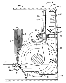
FIG. 1 is a side sectional view of a paper currency dispensing mechanism
showing a currency thickness indicator arrangement illustrating an aspect of
the
present invention; and
FIG. 2 is a drawing schematically illustrating the control circuit for the
currency thickness apparatus shown in FIG. 1.
Detailed Description of the Preferred Embodime t
Referring now to the drawings wherein the showings are for the purpose
of illustrating a preferred embodiment of the invention, and not for the
purpose
of limiting same, FIG. 1 shows a currency dispensing system 10 for dispensing
single sheets of media. Currency dispensing system 10 includes a friction
picker
mechanism 12 for removing single sheets of a sheet media, specifically
currency
designated "C" in the drawing, from a stack designated "S". Stack S is
contained
within a canister 14 which is partially shown in FIG. 1. Canister 14 has an
opening 16 at one end which exposes stack S to a picker roller 22 mounted for
rotation on a shaft 24. Picker roller 22 includes a high friction
circumferential
portion 26 and a low friction circumferential portion 28. Picker roller 22 is
positioned such that the circumference of roller 22 extends slightly into
opening
16 of canister 14. Shaft 24 is mounted within a frame or housing 30 containing
currency canister 14 and picker mechanism 12. Shaft 24 is driven by a stepper
motor (not shown) under the control of a computer which operates the currency
dispensing system 10 and picker mechanism 12.
Counter rotating rollers 34 are mounted on a shaft 36 to be disposed
adjacent picker roller 22. The outer surface of counter rollers 34 are in
close
proximity to, but do not contact, picker roller 22. Counter rollers 34 are
driven
by means (not shown). During normal operation picker roller 22 rotates in the
direction of arrow A and counter roller 34 rotates in the direction of arrow
B. A
plate 42 is mounted adjacent picker roller 22 and counter roller 34. Openings
in
plate 42 allow counter roller 34 to extend therethrough and allows a portion
of
r
picker roller 22 to intersect plate 42. Plate 42 defines a path, designated 44
in the
drawings, along which sheets C of currency are passed. A dispensing passage 46
is formed in housing 30 to discharge sheets S therefrom.
CA 02216968 2004-O1-14
-6-
Picker mechanism 12 includes a generally Y-shaped or wishbone-shaped
element 50. Y-shaped element 50 includes an upper leg portion 52 and two
spaced apart lower leg portions 54. Lower leg portions 54 are generally
hook-shaped as shown in FIG. I and are spaced apart to be positioned on
opposite sides of picker roller 22 with the hook-shaped portion extending
around
shaft 24. The free end of lower leg portions 54 have a contoured surface 56
adapted to engage plate 42 and to engage sheets S which pass therealong. At
the
midsection of Y-shaped element 50, i.e., at the junction where the lower legs
54
join with upper leg 52, a cavity 66 is formed therein. Cavity 66 is generally
cylindrical in shape and includes a spherical bottom 68. Cavity 66 is provided
to
receive an adjustable mounting pin 72 which has a semi-spherical end portion
74.
Semi-spherical end portion 74 is dimensioned to mate with spherical bottom 68
of cavity 66 wherein Y-shaped element 50 may freely pivot on mounting pin 72.
Pin 72 is attached to a threaded rod 76 which extends into a threaded bore 78
in
a post 82 which is formed or otherwise attached to housing 30. The position of
mounting pin 72 is thus adjustable along the axis of threaded rod 76. Above
mountin~t pin 72 a torsion spring 84 is attached to upper leg, portion 52 and
to
housing 30. Torsion spring 84 and compression spring are operable to urge
contoured surface 56 of lower leg portions 54 into engagement wtth plate 42.
A target 86, which in the preferred embodiment is a disk of metallic
material, is fixedly mounted to upper leg portion 52 so as to be integral and
movable therewith.
A sensor arrangement 90 is mounted to housing 30 adjacent target 86.
Sensor arrangement 90 acts as a signal generating means and is preferably the
type which generates a voltage signal proportional to the distance of the
plane of
the face of the metallic target 86 from sensor arrangement 90.
Referring now to FIG. 2, a schematic block diagram of sensor arrangement
90 is shown. Sensor arrangement 90 is generally comprised of a magnetic
proximity sensing device, designated 92 in the drawings, which changes its
operating characteristics when an object, specifically a metallic object,
comes near
it, such as Model No. 921H26Q manufactured by Micro Switch, a Division of
Honeywell Corporation of Illinois. Such a sensor produces an output voltage,
CA 02216968 1997-09-30
WO 96131425 PCT/US96/04299
_7_
designated "Vv' in the drawing, whose change is proportional to the relative
distance between the sensor and target 86. A portion of sensor circuit 92
includes
. a potentiometer 94 which is used during calibration of sensor 92 to set the
appropriate zero value or reference value. In this respect, the steady state
output
voltage Vo of sensor circuit 92 is adjustable, i.e., variable, by means of
potentiometer 94, the output of sensor circuit 92 however still being
proportional
to the relative distance between sensor circuit 92 and target 86 and added to
the
steady state value.
According to the present invention, a feedback control circuit 96 is added
to existing sensor circuit 92. Feedback control circuit 96 automatically
readjusts
the steady state voltage output Vo of sensing circuit 92 by generating an
input or
drive value, designated by Vl, to sensing circuit 92. Specifically, control
circuit 96
produces an input voltage VI replacing the one derived from the center tap of
voltage divider potentiometer 94. Input voltage VI from control circuit 96 is
based
upon the comparison between the actual steady state output voltage Vo of
sensing
circuit 92 and a desired setpoint or reference voltage designated VR. Control
circuit 96 compares the steady state actual output voltage Vo with the
reference
voltage VR and adjusts the input voltage VI to make the steady state output
voltage Vo equal to the reference voltage VR. As used herein the term steady
state output voltage Vo refers to the output voltage when no sheet media or
currency C is between countered surface 56 of Y-shaped element 50 and plate
42.
In this respect, as will be appreciated, as currency C passes between plate 42
and
contoured surface 56, voltage output Vo increases to reflect the change in
position
of target 86 relative to sensor arrangement 90. Thus, control circuit 96 is
adapted
to adjust input voltage Vl, and therefore, the steady state of the output
voltage Vo
only when a drop from the steady state output voltage of the circuit is
detected
in output voltage Vo.
.a
Control circuit 96 includes comparator means 102 for comparing the output
voltage Vo to the reference voltage VR, and further includes adjustment means
104 for adjusting the input voltage VI until the output voltage Vo equals the
reference voltage VR. Importantly, according to the present invention, control
circuit 96 adjusts the input voltage VI only when the idle or steady state
output
CA 02216968 1997-09-30
WO 96131425 PCT/US96104299
_g_
voltage Vo shows a gradual permanent change over time in one direction. For
example, control circuit 96 may be programmed or designed to adjust the input
voltage VI when the steady state output voltage Vo shows a gradual permanent '
reduction over time. For example, in the embodiment shown, sensing circuit 96
may have an operating range of 0 to 10 volts. The reference voltage Vo may be
set to 2 volts thereby provide an 8 volts range for the detection of thicker
media
or multiples of media. Previous systems had to have the steady state output
voltage Vo set to a higher value than 2 volts, say 5 volts, to allow for
deterioration
caused by part wear. This seduces the dynamic operating measurement range to
span only 5 to 10 volts, limiting the maximum media thickness measurement
capability. Control circuit 96 may be programmed or designed to adjust the
input
voltage VI only after the output voltage Vo drops below 1.95 volts. When the
output voltage drops below 1.95 volts, control circuit 96 adjusts input
voltage VI
to bring the steady state output voltage Vo to 2 volts or to a range near 2
volts,
e.g., 1.99 volts to 2.01 volts, or some other acceptable window.
In the embodiment shown, control circuit 76 is adapted to adjust the input
voltage VI when the output voltage Vo from sensor circuit 92 gradually
decreases.
The decrease is a result of target 86 moving slightly closer to sensing
circuit 92,
which movement is caused by surface 56 of Y-shaped element 50 gradually
wearing over time due to the sheets S repeatedly sliding thereagainst. In this
respect, large increases in the output voltage Vo of sensor circuit 92 are
attributable to currency passing between plate 42 and surface 56 of Iower leg
portion 54. Alternately, control circuit 96 may be designed or programmed to
adjust the input voltage VI only when the output voltage Vo exhibits a gradual
permanent voltage increase over time.
Control circuit 96 is preferably includes processing means (not shown) for
performing the comparison function and the voltage adjustment function. Memory
means 106 may also be provided to monitor the rate of adjustment and to
determine when the voltage input Vl adjustment has reached a predetermined
maximum amount whereafter further adjustment to the input voltage VI is '
prevented and a signal is provided that the maximum allowable adjustment has
been reached. In this respect, the adjustment limit indicates when excessive
wear
CA 02216968 2004-O1-14
-9-
of contoured surface 56 of lower leg portion 54 has occurred wherein the shift
of
target 86 relative to sensing circuit 92 may be beyond its operating range.
Referring now to the operation of the present invention, as sheets S are
dispensed from currency dispensing system 10 under the influence picker roller
22,
sheets C pass between plate 42 and contoured surface 56 of Y-shaped element
50.
The thickness of sheet C causes Y-shaped element 50 to pivot on mounting pin
72 causing target 86 to move relative to sensor circuit 92. The relative
movement
produces a voltage change in sensor arrangement 90 which is indicative of the
thickness of sheet C. A more detailed description of the operation of such an
arrangement may be found in U.S. Letters Patent No. 4,664,369 to Graef et al.,
Numerous and repeated dispensing of sheets C will eventually cause contoured
surface 56 of Y-
shaped element 50 to wear or erode away thereby causing target 86 to move
slightly closer to sensing circuit 92. As indicated in the Background of the
Specification, even minor changes in the position of target 86 produce
noticeable
deviations in the voltage output Vo of sensor circuit 92. According to the
present
invention, the gradual shifting of the neutral position of target 86 relative
to
sensor circuit 92 is compensated for by control circuit 96 which adjusts the
input
voltage Vl to sensor circuit 92 to maintain the steady state output voltage Vo
of
the sensor at a predetermined reference value VR. Thus, the wearing of
contoured surface 56 of lower leg portion 54 is electrically compensated for
by
control circuit 96.
Importantly, a system as defined above allows for high sensitivity
measurements of differential positions while maintaining a capability of a
large
dynamic measurement range. Any increase in the output voltage Vo of sensor
circuit 92 is attributed to medium measurement, and any gradual decrease in
the
voltage output Vo is attributed to mechanical wear, and the control circuit
adjusts
the input voltage V, of sensor circuit 92 back to the reference voltage VR.
With
the foregoing arrangement, the setpoint or reference point of the system can
be
chosen to be a much lower value than the previous system. This allows for
thicker
or larger multiples of media to be detectable over a larger range. In this
respect,
because the output voltage Vo of sensing circuit 92 is controlled to be at the
CA 02216968 1997-09-30
WO 96/31425 PCT/US96/04299
-10-
reference or setpoint voltage VR, it does not change with wear in the
mechanical
components which means that the dynamic measurement range remains constant.
Further, the actual value of the "adjustment" to the input voltage VI is a
direct
measurement of the distance target 86 has moved relative to sensing circuit 92
as
s
a result of wear. In this respect, the "adjustment" value can used as an
indication
of wear and to predict ultimate failure of the system. Importantly, by
producing
tho setpoint or reference point at a lower value with a larger dynamic range,
a
system according to the present invention is operable for longer periods of
time
without requiring mechanical readjustment of mounting pin 72 to bring a system
back into operable range.
It is intended that all such modifications and alterations be included insofar
as they come within the scope of the patent as claimed or the equivalents
thereof.