Note: Descriptions are shown in the official language in which they were submitted.
CA 02217083 1997-09-29
Q97-1032
SUSPENSION WITH MULTI-LAYERED INTEGRATED
CONDUCTOR T~ACE ARRAY FOR OPTIMIZED ELECTRICAL
PARAMETERS
Reference to Related Application
This is related to copending U.S. Patent Application Serial No.
08/720,836, filed on October 3, 1996, which is a continuation-in-part of
U.S. Patent Application Serial No. 08/621,431, filed on March 25, 1996, the
disclosure thereof being incorporated herein by reference.
Field of the Invention
This invention relates generally to structure and method for
controlling electrical impedance characteristics of a trace conductor array
formed integrally with a flexure of a head suspension assembly. More
particularly, the present invention relates to an integrated suspension and
conductor structure wherein the suspension traces are arranged and
configured in multiple layers so as to obtain, tune and control electrical
parameters, particularly inductance and/or capacitance.
Back~round of the Invention
Contemporary disk drives typically include a rotating rigid storage
disk and a head positioner for positioning a data transducer at different
radial locations relative to the axis of rotation of the disk, thereby defining
numerous concentric data storage tracks on each recording surface of the
disk. The head positioner is typically referred to as an actuator. Although
numerous actuator structures are known in the art, in-line rotary voice coil
actuators are now most frequently employed due to their simplicity, high
performance, and their ability to be mass balanced about their axis of
rotation, the latter being important for m~king the actuator less sensitive to
perturbations. A closed-loop servo system within the disk drive is
conventionally employed to operate the voice coil actuator and thereby
position the heads with respect to the disk surface.
An air bearing surface supports the transducer at a small distance
away from the surface of the moving medium. Single write/read element
CA 02217083 1997-09-29
Q97-1032
designs typically require two wire connections while dual designs having
separate reader and writer elements require four wire connections.
Magnetoresistive (MR) heads in particular generally require four wires. The
combination of an air bearing slider and a read/write transducer is also
5 known as a read/write head or a recording head.
Sliders are generally mounted to a gimbaled flexure structure attached
to the distal end of a suspension's load beam structure. A spring biases the
load beam and the head towards the disk, while the air pressure beneath the
lO head pushes the head away from the disk. An equilibrium distance defines
an "air bearing" and determines the "flying height" of the head. By utili7.in~
an air bearing to support the head away from the disk surface, the head
operates in a hydrodynamically lubricated regime at the head/disk interface
rather than in a boundary lubricated regime. The air bearing maintains a
15 spacing between the transducer and the medium which reduces transducer
efficiency. However, the avoidance of direct contact vastly improves the
reliability and useful life of the head and disk components. Demand for
increased areal densities may nonetheless require that heads be operated in
pseudo contact or even boundary lubricated contact regimes, however.
Currently, flying heights are on the order of 0.5 to 2 microinches.
The magnetic storage density increases as the head approaches the storage
surface of the disk. Thus, a very low flying height is traded against device
reliability over a reasonable service life of the disk drive. At the same time,
25 data transfer rates to and from the storage surface are increasing; and, data rates approaching 200 megabits per second are within practical
contemplation.
The disk drive industry has been progressively decreasing the size and
30 mass of the slider structures in order to reduce the moving mass of the
actuator assembly and to permit closer operation of the transducer to the
disk surface, the former giving rise to improved seek performance and the
latter giving rise to improved transducer efficiency that can then be traded
for higher areal density. The size (and therefore mass) of a slider is usually
35 characterized with reference to a so-called standard 100% slider
("minislider"). The terms 70%, 50%, and 30% slider ("microslider",
"nanoslider", and "picoslider", respectively) therefore refer to more recent
CA 02217083 1997-09-29
Q97-1032
low mass sliders that have linear dimensions that are scaled by the
applicable percentage relative to the linear dimensions of a standard
minislider. Smaller slider structures generally require more compliant
gimbals, hence the intrinsic stiffness of the conductor wires attached to the
s slider can give rise to a significant undesired bias effect.
To reduce the effects of this intrinsic wire stiffness or bias, integrated
flexure/conductor structures have been proposed which effectively integrate
the wires with an insulating flexible polymeric resinous flexure such that the
10 conductors are exposed at bonding pads positioned at the distal end of the
flexure in the proximity of the head. U.S. Patent No. 5,006,946 to
Matsuzaki discloses an example of such a configuration. U.S. Patent No.
5,491,597 to Bennin et al. discloses a further example in point. While such
wiring configurations do enjoy certain performance and assembly
15 advantages, the introduction of the disclosed flexible polymeric resinous
material in the flexure and gimbal structure raises a number of challenging
design issues. For example, the thermal expansion properties of the
resinous material is not the same as the prior art stainless steel structures;
and, the long-term durability of such resinous structures, including any
20 requisite adhesive layers, is unknown. Therefore, hybrid stainless steel
flexure and conductor structures have been proposed which incorporate
most of the benefits of the integrated conductor flex-circuit flexure
structures while rem~ining largely compatible with prior art fabrication and
load beam attachment methods. Such hybrid designs typically employ
2s stainless steel flexures having deposited insulating and conductive trace
layers for electrical interconnection of the head to the associated drive
electronics, e.g., a proximately located preamplifier chip and downstream
read channel circuitry typically carried on a circuit board (along with other
circuitry) attached to the head/disk assembly.
As taught by U.S. patent No. 5,491,597 to Bennin et al., entitled:
"Gimbal Flexure and Electrical Interconnect Assembly", the disclosed prior
approach called for use of a spring material for the conductive trace layers,
such as beryllium-copper alloy, which admittedly has higher electrical
3s resistance than pure annealed copper, for example. On the other hand, pure
armealed copper, while a satisfactory electrical conductor at high
frequencies, also manifests high ductility rather than spring-like mechanical
CA 02217083 1997-09-29
Q97-1032
resilience, and therefore lacks certain mechanical spring properties desired
in the interconnect trace material. Traces formed of pure copper plated or
deposited onto e.g. a nickel base layer provide one alternative to the
beryllium-copper alloy relied upon by the Bennin et al. approach.
s
These hybrid flexure designs employ relatively lengthy runs of
conductor trace pairs or four-wire sets which extend from bonding pads at
the distal, head-mounting end of the flexure to the proximal end of the
flexure, to provide a conductive path from the read/write head along the
10 length of the associated suspension structure to the preamplifier or read-
channel chip(s). Because the conductor traces are positioned extremely
close to, but electrically isolated from, the conductive stainless steel flexurestructure which is in turn grounded to the load beam, and because of the
relatively high signal rates being transferred, the conductor trace inductance
15 and mutual coupling, as well as conductor trace resistance and trace
capacitance to ground, can give rise to unwanted signal reflections,
distortion, and inefficient signal/power transfer. The unwanted signal
reflections tend to deleteriously affect the performance of the read/write
head, interconnect structure, and driver/preamplifier circuit.
Micro strip line technology teaches that the loop and inter-conductor
capacitance may be changed by ch~n~in~ the dimensions of and/or spacing
between micro strips forming a transmission line. However, in the case of
integrated trace array wiring schemes for use with head suspension load
2s beams, the dimensions of the conductors are governed by mechanical
constraints including the space available on the flexure for the trace
interconnect array, and the trace conductor dimensions cannot be changed
very much insofar as impedance matching or tuning is concerned.
While the Bennin et al. '597 patent discussed above includes an
embodiment of Figs. 6-8 calling for stacking of traces to form a multi-level
array of trace sets, there is no teaching of using conductor traces arranged in
multi-level arrays in order to obtain desired electrical parameters, such as
capacitance and/or inductance, for example.
3s
The invention to be described provides, inter alia, a flexure for a
suspension in a disk drive which includes a multiple layered integrated
CA 02217083 1997-09-29
Q97-1032
conductor array having reduced resistance and controllably tuned
inductance and capacitance parameters in order to improve trace array
electrical performance.
S S-lmm~ry of the Invention with Objects
A general object of the present invention is to provide a low-profile,
robust and reliable high performance suspension assembly having a multi-
layered integral conductor trace array for electrically interconnecting a
10 read/write head to associated read/write circuitry which overcomes
limitations and drawbacks of the prior art.
Another general object of the present invention is to provide an
integrated suspension and conductor structure having controlled multiple
15 layer trace geometries relative to a ground plane in a manner achieving
improved micro-strip signal transmission line characteristics thereby
overcoming limitations and drawbacks of the prior art.
A more specific object of the present invention is to provide a method
20 for reducing resistance, and for controlling capacitance, mutual inductance
and overall impedance of an integrated flexure/multi-layered conductor
structure for use with a read/write head in a disk drive.
Still another object of the present invention is to provide an integrated
25 flexure and multi-layer conductor trace array providing separate
optimi7~tion of capacitance and inductance of the conductors of both the
read and the write elements of a dual-element read/write head.
Another object of the present invention is to provide an improved
30 suspension and multi-layer conductor trace array for supporting and
electrically connecting to read/write head elements carried on a slider in a
hard disk drive.
A suspension assembly in accordance with principles of the present
35 invention includes a flexure having a multiple-layer integrated trace
conductor array along the flexure. The multi-layer conductor traces replace
prior art discrete twisted wire pairs which would normally extend along the
CA 02217083 1997-09-29
- Q97-1032
length of the associated suspension. The conductor trace geometry and
relative location in a multiple layer trace array relative to the flexure groundplane and to other traces enables control of inter-trace capacitance, balance
of trace capacitance to ground, and reduction of trace inductance parameters
5 over other approaches, thereby enabling a particular electrical parameter to
be effectively tuned to achieve a desired operating condition. The
invention provides improved electrical performance in a multi-layer trace
conductor array without materially altering suspension design or adversely
affecting the suspension's mechanical performance.
In one preferred form, an integrated flexure/conductor structure
supports a read/write head adjacent to a storage medium and electrically
interconnects the head to read/write circuitry. In this approach the
flexure/conductor structure includes a generally planar conductive flexure
15 member having a gimbal for supporting the read/write head. A first
electrical insulation layer is formed on the flexure member. A first electrical
trace path is formed on the first electrical insulation layer. A second
electrical insulation layer is formed on the first electrical trace path. A
second electrical trace path is formed on the second electrical insulation
20 layer. In this approach the second electrical trace path is laterally offset
relative to the first electrical trace path in order to control and reduce inter-
trace electrode capacitance, while minimi7.in~ increase in inductance ofthe
trace array.
In an alternative preferred form, an integrated load beam assembly
supports a read/write head/slider assembly adjacent to a storage medium and
electrically interconnects the head to read/write circuitry. The load beam
assembly comprises a generally planar conductive member extending to
proximity of the read/write head/slider assembly; a first electrical insulation
layer disposed on the conductive member; at least one electrical trace path
disposed on the first electrical insulation layer; and, a ground plane
structure connected to the generally planar conductive member and
disposed in overlying and surrounding relation, and spaced away from, the
at least one electrical trace path to form a multi-layer shielded transmission
line structure.
CA 02217083 1997-09-29
Q97-1032
In another preferred form, an integrated flexure/conductor structure
supports a read/write head/slider assembly adjacent to a storage medium and
electrically interconnects the head to read/write circuitry. In this approach
the flexure/conductor structure also comprises a generally planar conductive
S flexure member having a gimbal for supporting the read/write head/slider
assembly. A first electrical insulation layer is formed on the flexure
member. First and second electrical trace paths are formed on the first
electrical insulation layer. A second electrical insulation layer is formed on
the first and second electrical trace paths. Third and fourth electrical trace
10 paths are formed on the second electrical insulation layer. The third and
fourth electrical trace path are laterally offset relative to each other and arelongitudinally aligned with and overlying respectively the first and second
electrical trace paths; and, the first electrical trace path is connected in
parallel with the fourth electrical trace path, and the second electrical trace
15 path is connected in parallel with the third electrical trace path, thereby
equ~ ing trace path capacitance to a ground plane provided by the flexure
member.
In a further preferred form, an integrated flexure/conductor structure
20 supports a read/write head/slider assembly adjacent to a storage medium and
electrically interconnects the head to read/write circuitry. The
flexure/conductor structure comprises a generally planar conductive flexure
member having a gimbal for supporting the read/write head/slider assembly.
A first electrical insulation layer is disposed on the flexure member. First
2s and second electrical trace paths are disposed on the first electrical
insulation layer in a laterally spaced apart relation. A second electrical
insulation layer is disposed on the first and second electrical trace paths.
Third and fourth electrical trace paths are disposed on the second electrical
insulation layer in a laterally spaced apart relation. A third electrical
30 insulation layer is disposed on the third and fourth electrical trace paths.
Fifth and sixth electrical trace paths are disposed on the third electrical
insulation layer in a laterally spaced apart relation. In this arrangement the
first, third and fifth electrical trace paths are longitl-~lin~lly and laterallyaligned relative to each other and are electrically connected in parallel to
3s form a supply path, while the second, fourth and sixth electrical trace pathsare longitudinally and laterally aligned relative to each other and are also
connected in parallel to form a return path, thereby reducing inductance
CA 02217083 1997-09-29
Q97-1032
without substantially increasing inter-electrode capacitance between the
supply path and the return path. Other trace paths and layers may be added
to this structure in order further to reduce trace array inductance.
These and other objects, advantages, aspects, and features of the
present invention will be more fully appreciated and understood upon
consideration of the following detailed description of preferred
embodiments presented in conjunction with the accompanying drawings.
Brief Description of the Drawin~s
In the Drawings:
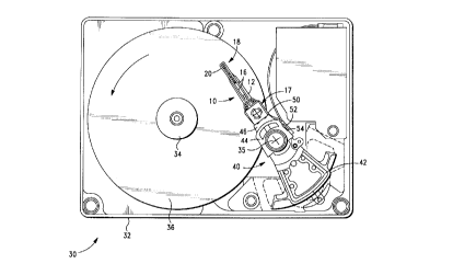
Fig. 1 is an enlarged, diagr~mm~tic plan view of a disk drive
15 including a suspension assembly having a multi-layer conductive trace array
incorporating principles of the present invention.
Fig. 2 is an enlarged diagr~mm~tic plan view of a first preferred
embodiment of integrated flexure/conductor load beam structure having
20 tuned conductive traces in accordance with principles of the present
inventlon.
Fig. 3 is an enlarged plan view of a flexure of the Fig. 2 load beam
structure having integral wiring incorporating the tuned conductive trace
25 array.
Fig. 3A is a greatly enlarged plan view of a read/write head
connection region of the Fig. 3 flexure trace array and wherein the head
slider is shown in dashed line outline.
Fig. 3B is a greatly enlarged view in elevation and cross-section taken
along section line 3B-3B in Fig. 3.
Fig. 3C is a greatly enlarged view in perspective of a slider end of the
35 Fig. 2 load beam structure showing the slider attached to the flexure gimbal,and showing electrical gold ball connections between the flexure trace array
and the read/write head connection pads of the slider.
CA 02217083 1997-09-29
Q97-1032
Fig. 4A is a greatly enlarged diagr~rnm~tic view in elevation and
cross section of an embodiment of the invention alternative to the one
shown in Fig. 3B, showing the traces to be laterally offset in order to tune
5 inductance and inter-trace capacitance parameters.
Fig. 4B is a variant trace geometry of the Fig. 4A embodiment,
showing the traces fully displaced laterally so that there is no actual overlap
between the traces of the plural trace layers.
Fig. 4C is an enlarged diagr~mm~tic view in elevation and cross
section of another embodiment of the invention which is similar to the
embodiment of Figs. 4A and 4B, with the signal paths being formed as a
series of interleaved and offset traces.
Fig. SA is a graph of data plotting inter-conductor capacitance as a
function of controlled trace overlap as shown in Figs. 4A and 4B.
Fig. SB is a graph of data plotting trace inductance as a function of
20 controlled trace overlap as shown in Figs. 4A and 4B.
Fig. SC is a graph of data plotting characteristic impedance of the
micro-strip transmission line of Figs. 4A and 4B as a function of trace
conductor overlap in a two-layer geometry.
Fig. 6 is a greatly enlarged diagr~rnm~tic view in elevation and cross
section of another embodiment of the invention alternative to the ones
shown in Fig. 3B and Figs. 4A and 4B. In this embodiment the multiple
layers of traces include multiple layers of dielectric films between trace
30 layers.
Fig. 7A is a graph of data plotting resistance as a function of the
number of parallel trace conductors in a trace array of the type shown in Fig.
6.
CA 02217083 1997-09-29
Q97-1032
Fig. 7B is a graph of data plotting inductance as a function of the
number of parallel trace conductors in a trace array of the type shown in Fig.
6.
S Fig. 7C is a graph of data plotting capacitance as a function of thenumber of parallel trace conductors in a trace array of the type shown in Fig.
6.
Fig. 8 is a greatly enlarged diagr~rnm~tic view in elevation and cross
section of a further embodiment of the invention alternative to the
embodiments of Figs.3B,4A-B and 6, wherein trace conductor parallel path
pairs are laterally spaced and aligned with second parallel path pairs in order
to equalize capacitance to the flexure substrate.
Fig. 9 is a greatly enlarged diagr~mm~tic view in elevation and cross
section of yet another self-shielding embodiment of the invention alternative
to the one shown in Fig.3B, wherein the traces are shown in a middle layer
of a multiple layer trace array and wherein lower and upper traces form a
Faraday (electrostatic) shield around the active service loop kace pairs.
Detailed Description of Preferred Embodiments
Referring to the drawings, where like characters designate like or
corresponding parts throughout the views, Fig. 1 presents a diagr~rnm~tic
top plan view of a head/disk assembly (HDA) of a hard disk drive 30. The
hard disk drive 30 employs at least one load beam assembly 10 having a
flexure 14 including a trace interconnect array 16 as a first preferred
embodiment of the present invention. Fig.1 shows the load beam assembly
10 with the flexure 14 and trace interconnect array 16 employed within its
intended operating environment.
In the present example disk drive 30 includes e.g. a rigid base 32
supporting a spindle 34 (and spindle motor, not shown) for rotating at least
one storage disk 36 in a direction shown by the curved arrow. Drive 30
also includes a rotary actuator assembly 40 rotationally mounted to the base
32 at a pivot point 35. The actuator assembly 40 includes a voice coil 42
which, when selectively energized by control circuitry (not shown), moves
CA 02217083 1997-09-29
Q97- 1032
and thereby positions an actuator E-block 44 and head arms 46 (and load
beam assemblies 10) at radial track positions defined on the facing surfaces
of storage disks 36. At least one of the load beam assemblies 10 is secured
at its proximal end 17 to a distal end of a head arm 46, e.g. by conventional
ball-swaging techniques.
Conventionally, but not necessarily, two load beam assemblies 10 are
attached to head arms 46 between disks 36; and, one load beam structure 10
is attached to head arms above and below the uppermost and lowermost
disks of a disk stack comprised of multiple disks 36 spaced apart on spindle
34. The interconnect structure 16 connects to a flexible trace/film segment
50 which extends to a ceramic hybrid circuit substrate 52 secured to a side
of the E-block 44. The ceramic hybrid circuit 52 secures and connects a
semiconductor chip 54 forming a read preamplifier/write driver circuit.
Most preferably, the chip 54 is nested between the ceramic substrate of the
hybrid circuit 52 and the E-block sidewall, and is secured to the sidewall by
a suitable conductive adhesive or thermal transfer compound such that heat
generated during operation of the chip 54 is dissipated into the E-block by
conduction, and outwardly into the ambient air volume by convection.
As shown in Figs. 2,3,3A, 3B and 3C, the load beam assembly 10
includes a generally planar formed stainless steel load beam 12 and a flexure
14. In the present example, the flexure 14 is formed ofthin stainless steel
sheet material which is e.g. approximately 20-microns thick. An array of
two pairs of conductive traces 60 and 62 of approximately 10-microns thick
copper conductor forms part of an interconnect structure 16 which extends
from the proximal end 17 of flexure 14 to another connection pad array 22
located at the slider-supporting distal end 18 of the load beam assembly 10.
A transducer head slider 20 is attached to the gimbal 14 by a suitable
adhesive at the distal end 18 of the load beam structure 10. As shown in
Fig. 3C the connection pads 22 at the distal end 18 are provided for
connection by e.g. ultrasonically-welded gold ball bonds 56 to aligned
connection pads 24 of a dual-element (four conductor) thin film magneto-
resistive read/write structure 26 formed on a trailing edge of the slider body
20. Preferably, although not necessarily, the slider body 20 is a 30% slider.
CA 02217083 1997-09-29
Q97-1032
Interconnect structure 16 includes a high dielectric polyimide film
base 25 interposed between the conductive traces 60 and 62 of the
conductor array 16 mounted to the stainless steel flexure 14. The dielectric
layer is preferably about 10-microns thick. In accordance with principles of
the present invention, the flexure 14, in addition to providing a gimbal
mounting for the read/write head, defines one or more openings or troughs
28 of controlled width (w) and placement relative to the conductive traces
60 and 62 ofthe conductor structure 16 These longitllclin~l openings 28
defined along flexure 14 are arranged and spaced relative to the conductor
array 16 in a manner enabling e.g. inductance, capacitance and resistance
components of line impedance of the conductor structure to be tuned by
varying the width dimension (w) relative to the array 16 as discussed
hereinafter in connection with Figs. 7A, 7B and 7C. Accordingly, the
present invention provides a method for tuning and controlling the electrical
properties of impedance, including inductance, capacitance and resistance
components, of the conductor array 16 arising from integration thereof with
the stainless steel flexure 14.
At high data signal frequencies the interconnect structure 16 behaves
as a micro strip transmission line for carrying the signals passing between
the read/write head and read/write preamplifier/driver chip 54. Accordingly,
the geometry of the openings or recesses 28 is also an important factor for
controlling impedance along the signal path of trace conductor structure 16,
as discussed hereinafter in connection with Figs. 6A-6D.
2s
As shown in Fig. 3B, interconnect array 16 includes, in this
embodiment, at least one pair of conductive traces 60 and 62 which are
arranged overlay alignment in two layers of the interconnect trace array 16.
A first insulating polyimide (a flexible polymeric resinous material) layer 25
isolates the first (inner) trace 60 from the thin stainless steel flexure 14. A
second insulating polyimide layer 27 separates and electrically isolates the
first trace 60 from a second (outer) trace 62. Although not strictly required,
an additional insulation layer of about 4-microns thickness (not shown) may
be provided to protect the trace 62. Since the thickness dimension of the
dielectric layer 27 between the traces 60 and 62 is on the order of 10
microns in the present example, the inductance is greatly reduced, which
may be very desirable, particularly for current carrying trace pairs leading to
CA 02217083 1997-09-29
Q97-1032
an inductive write element in the head structure. On the other hand, the Fig.
3B arrangement creates significantly greater inter-trace conductor
capacitance levels than present when the traces are arranged in a side-by-
side arrangement with e.g. a minimum separation along adjacent trace edges
S of approximately 10microns.
Figs. 4A and 4B illustrate a variation upon the Fig. 3B multi-layer
arrangement. In Figs. 4A and 4B, the inner conductor 60 has been laterally
displaced to the side of the outer conductor 62. This arrangement
10 controllably reduces inter-trace capacitance. The amount of lateral
displacement or offset of the inner trace 60 relative to the outer trace 62 may
be used to tune or reduce the inter-trace capacitance in order to reach an
acceptable level. In this example, the conductor traces are e.g. 100 microns
wide. Figs. 5A, SB and SC present the changes respectively in capacitance,
l S inductance and impedance as a function of overlap, wherein 100 microns
represents complete overlap of the traces 60 and 62 as shown in Fig. 3B, and
0 represents complete lateral separation of the traces 60 and 62 as shown in
Fig. 4B. Capacitance effects to the flexure 14 are not considered in this
present discussion.
As can be seen from Figs. SA, SB and SC, the inductance when the
trace conductors overlap completely is about 8 nanoHenrys, which is
significantly lower than inductance present when the traces of the same
dimensions are arranged in a side-by-side arrangement in a single trace layer
2s (14 nanoHenrys). However, the capacitance in the Fig.3B case is much
higher than the inter-trace electrode capacitance present in the side-by-side
single layer arrangement. By partially overlapping the conductors, an
acceptable level of inter-trace capacitance may be obtained while
significantly reducing the trace inductance. For example, for SpF of
30 capacitance, the inductance from a trace array of the Fig. 4A type having a
20 micron overlap is 14 nH, while in a side-by-side arrangement, the
inductance would be 20 nH. Thus, the arrangements of Figs.3B, 4A and 4B
provide not only very low values of inductance, for a given amount of inter-
electrode capacitance, a lower value of inductance is obtained.
One way to reduce inter-electrode capacitance even more is shown in
Fig. 6. In this embodiment there are three trace layers: a first layer (traces
CA 02217083 1997-09-29
Q97-1032
60A and 62A), a second layer (traces 60B and 62B) and a third layer (traces
60C and 62C), separated respectively from the flexure 14 and from each
other by three dielectric layers 25, 27 and 29. The conductors 60A, 60B and
60C of the three layers are connected in parallel, while the conductors 62A,
62B and 62C are also connected in parallel. In this example, the parallel
conductors 60A, B and C provide a supply path, whereas the parallel
conductors 62A, B and C provide a return path. Since parallel conductors
create individual inductance in parallel, the overall inductance is reduced.
The arrangement of Fig. 6 may be extended to any number of layers that
may be practically formed, given process considerations and manufacturing
costs, as well as acceptable mechanical properties in the final load
beam/flexure structure.
Figs. 7A, 7B and 7C respectively graph high frequency resistance,
inductance and capacitance as a function of the number of trace layers of the
array. Even with a six-trace layer configuration of the Fig. 6 type, the
capacitance between supply and return path trace conductors is below S pF,
and the inductance is at 13 nH, wherein the conductive traces are only 30
microns wide. By increasing the width of the individual trace conductors,
the inductance can be further reduced, with a nominal increase in inter-
conductor capacitance. One difference between the operating conditions of
the Fig. 6 trace array and the Figs. 3B, 4A and 4B trace arrays is that in the
Fig. 6 arrangement the currents above and below each dielectric layer are in
the same direction, whereas the currents in the Figs. 3B, 4A and 4B arrays
2s above and below the dielectric layer 27 are in the opposite directions.
The micro-strip configuration 16 shown in Fig. 3B is characterized by
low inductance, since the spacing between the current-carrying traces 60 and
62 is a function of the thickness of the dielectric layer 27 separating the
layers of traces 60 and 62. Since the traces of Fig. 3B are planar in nature,
the illustrated arrangement achieves significant reduction of inductance
when compared to a conventional side-by-side trace conductor arrangement.
One drawback already mentioned with the Fig. 3B trace array 16 is that the
conductive traces 60 and 62 have a capacitance to ground which is a
3s function of the distance of the conductors from the ground plane provided
e.g. by flexure 14. (This capacitance is largely removed by removal of
flexure material under the conductors and by placement of the conductors in
14
CA 02217083 1997-09-29
Q97-1032
a side-by-side array as described in the related application identified above
(U.S. Application Serial No. 08/720,836)). Since the Fig. 3B trace
conductor array has the two conductive traces 60 and 62 in lateral
registration with each other, the capacitance to ground of the outer trace 62
5 is much lower than the capacitance to ground of the inner trace 60. This
imbalance in capacitance to ground leads to a serious mismatch between the
conductor characteristics when the Fig. 3B configuration is used as a
balanced transmission line for a differential circuit.
The arrangement shown in Fig. 8 provides a multi-layer trace
arrangement which elimin~tes the ground plane capacitance mismatch
present in the Fig. 3B array. In the Fig. 8 trace array each conductor 60 and
62 is divided into two trace paths, 60A, 60B and 62A, 62B, there being four
trace paths in the array for a signal supply and return circuit (read or write
element). Each path 60 and 62 has a trace path (traces 60A and 62B) in an
inner layer separated by dielectric layers 25 and 27, and each path also has a
trace path (traces 62A and 60B) in an outer layer separated by dielectric
layer 27. The net trace capacitance to the ground plane provided by flexure
14 is therefore balanced between the trace paths 60 and 62, and any
mismatch due to capacitance to ground is elimin~ted.
As an example, if the micro-strip configuration of Fig. 3B extends for
a length of 57 mm, with conductors that are 60 microns wide, and with the
conductive traces 60 and 62 as well as the dielectric layers 25 and 27 all
being 10 microns thick, the capacitance to ground for the outer conductive
trace 62 is 1.70 pF, while the capacitance to ground for the inner conductive
trace 60 is 11.80 pF. When the geometry of Fig. 3B is replaced with the
geometry of Fig. 8, and wherein the widths of the trace segments 60A, 60B,
62A, and 62B are 30 microns, and stacked traces 60A and 62A are separated
laterally from stacked traces 62B and 60B by 30 microns, and with the same
conductor and dielectric layer thicknesses, the capacitance to ground for
each conductor 60 and 62 is 8.35 pF. Thus, the Fig. 8 trace array is seen to
equalize the capacitance to ground between the supply path 60 and the
return path 62. While the Fig. 8 trace array illustrates a single signal loop
having a supply and a return path, multiple loops may be obtained by
replicating the Fig. 8 array in any desired number of service loop paths.
CA 02217083 1997-09-29
Q97-1032
Fig. 9 significantly lowers capacitance of the Fig. 8 structure by
dividing the enveloping flexure shield material into trace segments
interleaved above and below signal conductor traces and laterally offset
from the signal conductor traces, in order to minimi7e inter-trace
5 capacitance. Fig. 9 shows a trace element array 16B formed as three trace
layers separated by two dielectric layers 27 and 29. (The dielectric layer 25
between the flexure 14 and the lowermost or innermost layer is omitted in
the Fig. 9 view for simplicity). In the Fig. 9 approach, discrete ground
traces 64, 66 and 68 are formed and used, rather than an unbroken conductor
10 sheet in order to reduce capacitance to the service loop pairs 60A-60B, and
62A-62B, and to the ground plane, not shown. Ground trace patterns 64 and
66, respectively below and above, are laterally offset from the service trace
pairs 60A-60B and 62A-62B. Ground traces 68 are formed in the same
trace layer as the active service trace pairs 60A-60B and 62A-62B.
The trace array structure is conventionally formed by any suitable
patterning technique, whether by way of photolithography and selective
etch, or by selective deposition, l~rnin~tion or attachment of the conductive
traces to the dielectric layers with adhesives, etc.
Those skilled in the art will recognize that, in accordance with the
principles of the invention, advanced dual element transducer designs (such
as an MR head 26 of Fig. 3C) may have the capacitance and/or impedance
of the signal paths of the read and write elements separately optimized by
25 employing different conductor geometries and arrangements for the read
and write conductive trace array segments, respectively.
Although the present invention has been described in terms of the
presently preferred embodiment, i.e., a deposited conductor flexure structure
30 which implements a gimbal, it should be clear to those skilled in the art that
the present invention may also be utilized in conjunction with, for example,
an integrated gimbal load beam structure, or other conductive suspension
members having proximately mounted, deposited, or embedded conductors
with or without ins~ ting overcoatings. Thus, it should be understood that
35 the instant disclosure is not to be interpreted as limiting. Various alterations
and modifications will no doubt become apparent to those skilled in the art
after having read the above disclosure. Accordingly, it is intended that the
16
CA 02217083 1997-09-29
Q97-1032
appended claims be interpreted as covering all alterations and modifications
as fall within the true spirit and scope of the invention.