Note: Descriptions are shown in the official language in which they were submitted.
CA 02218121 1997-10-08
Waveguide Grating Router Having Relatively Small Dimensions
Back-Jround of the Invention
1. Field of the Invention
The present invention relates generally to fiber optic communications networks,
s and, more particularly, to communications networks that include passive components for
routing and distributing optical signals of different wavelengths.
2. Related Art
Waveguide grating routers are typically utilized in the context of optical
wavelength division multiplexing (WDM). Numerous applications, far beyond
0 simultaneously multiplexing and demultiplexing received optical signals, have been
provided by monolithically integrating these routers with optical lasers, receivers, and
switches. Unfortunately, the large size of conventional waveguide grating routerstructures has placed severe limitations on the number of useful devices that may be
fabricated onto a single substrate. Moreover, the performance of existing waveguide
S grating router configurations is typically degraded due to variations in the spatial
refractive index across the semiconductor wafer. Such variations are generally
attributable to crystallographic growth and processing non-uniformities.
One illustrative example of a prior art waveguide multiplexer/demultiplexer is
shown in FIG. 1. FIG. 1 is a schematic drawing of a conventional waveguide
20 multiplexer/demultiplexer (MUX/DEMUX) 10 comprising a set of N input ports
indicated generally at 12, a first free space region 14, a waveguide grating array 16, a
second free space region 18, and a set of N output ports 20.
The fabrication of MUX/DEMUX structures such as the one depicted in FIG. 1
is shown and described in a paper by Martin Zirngibl et al. entitled "Demonstration of a
25 15 X 15 Arrayed Waveguide Multiplexer on InP", EEE Photonics Technology Letters,
Vol. 4, November, 1992, pp. 1250-1252. The structure shown in FIG. 1 can be
CA 02218121 1997-10-08
fabricated on a two-inch wafer of InP having a thickness of approximately 600 ~lm by
epitaxially growing a 0.4 llm thick, graded-index quaternary waveguide layer finished by
an 0.04 llm rib layer. The device may be photolithographically defined, and the rib layer
etched, to form the input ports, free space regions, grating array, and output ports,
s thereby providing the arrangement illustrated in FIG. 1. Finally, the structure may be
covered with epitaxial growth, using an InP cladding layer of approximately 2 llm.
In operation, light em~n;~ting from one of the input ports 12 into the free space
region 14 is collected by the dispersive waveguide grating arms of array 16. As will be
readily ascertained by those skilled in the art, a constant path length difference between
o adjacent grating arms causes a wavelength dependent phase shift. This linear phase
progression affects the propagation direction of the converging wave radiated in the
second free space region 18 toward the output ports 20.
As can be seen in FIG. 1, there is a substantial amount of unused space enclosedby the waveguide grating array 16 and free space regions 14 and 18. Accordingly,5 various approaches have been advanced to reduce the size of waveguide grating routers.
For example, in the case of InP waveguide grating routers, prior art approaches have
focused on size reduction by employing high contrast waveguides to enable a tight bend
radius of curvature. However, the bend radius is not the only parameter that determines
the size of the waveguide grating router. For example, there are two free-space regions
20 in the waveguide grating router that must be of sufficient length so as to allow the light
to be spread sufficiently, thereby per~nitting the light to be captured by the waveguides of
the dispersive waveguide grating.
Although various approaches have been advanced in the prior art to provide
waveguide grating routers having small dimensions, any benefits obtained by smaller size
25 are offset by either a significant deterioration in device performance, or by such stringent
processing tolerances so as to render their use economically unfeasible. By way of
illustration, in an article by H. Bissessur et al. entitled "Small-Size, Polarisation-
CA 02218121 1997-10-08
Independent Phrased-Array Demultiplexers on InP", Electronics Letters, vol. 31, pp.
2118 - 2119, (1995), there is described a compact demultiplexing and multiplexing
device in which a highly confined waveguide structure is utilized. In this device, a high
refractive index differential is realized by forming semiconductor-to-air interfaces. As
s will be readily appreciated by those skilled in the art, such a device can only be obtained
by rigidly controlling tolerances during the fabrication process. Because of this,
consistently adequate yields, as would be required for the production of commercial
quantities of the device, are difficult to achieve. What is needed is a waveguide grating
router of smaller size than that provided by prior art designs and which minimi7es and/or
0 e~iminates the shortcomings of prior art designs.
Summarv of the Invention
A compact waveguide grating router is constructed by forming at least first and
second free space regions, first and second sets of optical ports, and a grating array, onto
a substrate.. The grating array is coupled to the first free space region and the second
15 free space region. A first plane defining a first reflective surface is introduced into the
first free space region, and a second plane defining a second reflective surface is
introduced into the second free space region. The first plane is oriented such that
incident optical signals from the first set of optical ports are reflected to the grating
array, and the second plane is oriented such that incident optical signals from the grating
20 array are reflected to the second set of optical ports. The first and second planes are
provided, for example, by cleaving, cutting, etching, sawing, or any other suitable
technique. The first and second planes enable the input and output ports to be folded
back into previously unoccupied space. The aforementioned techniques enable the size
of any conventional waveguide grating router to be substantially reduced.
2s According to a further embodiment, a third plane is oriented in a direction such
that this plane passes through both the first free space region and the second free space
region, and such that the third plane is substantially perpendicular to the first and second
CA 02218121 1997-10-08
planes. The third plane defines an optically-reflective surface and may be introduced, for
example, by cleaving, cutting, etching, sawing, or any other suitable technique.
An alternate embodiment provides a compact waveguide grating router by
forming a first free space region, a first set of optical ports, and a grating array, onto a
s substrate.. The grating array is coupled to the first free space region. A first plane
defining a first reflective surface is introduced into the first free space region. The first
plane is oriented such that incident optical signals from the first set of optical ports are
reflected to the grating array. A second plane defining a second optically reflective
surface is oriented in a direction such that this plane passes through the first free space
0 region, and such that the second plane is substantially perpendicular to the first plane. A
third plane defines a third optically reflective surface, and is oriented across the
waveguide grating in a direction substan~ially perpendicular to the direction in which
optical energy traverses the waveguide grating. The first, second, and third planes are
provided, for example, by cleaving, cutting, etching, sawing, or any other suitable
5 technique. The first, second, and third planes enable the input and output ports to be
folded back into previously unoccupied space, thereby providing a waveguide grating
router of relatively compact dimensions.
Brief Description of the Drawin~
Other advantages and features of the invention will be readily apparent from the20 following description and to the accompanying drawings, in which:
FIG. 1 is a schematic drawing of a prior-art waveguide grating router;
F~IG. 2 is a schematic drawing of a waveguide grating router constructed
according to a first embodiment and employing first and second optically reflective
planes.
CA 02218121 1997-10-08
FIG. 3 is a schematic drawing of a waveguide grating router constructed
according to a second embodiment and employing first, second, and third optically
reflective planes.
FIG. 4 is a schematic drawing of a waveguide grating router constructed
s according to a third embodiment and employing first, second, and third optically
reflective planes.
FIG. 5 is a schematic drawing of a waveguide grating router constructed
according to a fourth embodiment and employing first and second optically reflective
planes.
o Detailed DescriPtion of the Invention
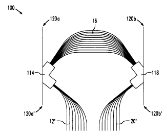
FIG. 2 is a schematic drawing of a waveguide grating router 100 constructed
according to a first embodiment . Waveguide grating router 100 may depict, for
example, an N by N multiplexer/demultiplexer structure that is constructed in roughly the
same manner as the structure 10 depicted in FIG. 1, but with two notable structural
differences: the use of a first plane 120a-120a', and a second plane 120b-120b'.Although the structure of FIG. 2 is shown with first plane 120a-120a' and second plane
120b- 120b', this is for purposes of illustration. The structure of FIG. 2 may,
alternatively, be fabricated using first plane 120a-120a' without using second plane
120b-120b'. Still alternatively, the structure of FIG. 2 may be fabricated using second
20 plane 120b-120b' without using first plane 120a-120a'.
Referring now to FIG. 2, a compact waveguide grating router 100 is constructed
by forming at least a first free space region 114, a second free space region 118, a first
set of optical ports 12', a second set of optical ports 20', and a grating array 16, onto a
substrate.. The grating array 16 is coupled to the first free space region 114 and the
second free space region 118. A first plane 120a-120a' defining a first reflective surface
is introduced into the first free space region 114, and a second plane 120b-120b' defining
a second reflective surface is introduced into the second free space region 118.
S
CA 02218121 1997-10-08
The first plane 120a-120a' is oriented such that incident optical signals from the
first set of optical ports 12' are reflected to the grating array 16, and the second plane
120b-120b' is oriented such that incident optical signals from the grating array 16 are
reflected to the second set of optical ports 20'. The first and second planes 120a-120a',
s 120b-120b' are provided, for example, by cleaving, cutting, etching, sawing, or any other
suitable technique. The first and second planes 120a-120a', 120b-120b' enable the input
and output ports to be folded back into previously unoccupied space. As will be
immediately recognized by those skilled in the art, the aforementioned techniques enable
the size of any conventional waveguide grating router to be reduced substantially.
0 FIG. 3 is a schematic drawing of a waveguide grating router 200 constructed
according to a second embodiment and employing first, second, and third optically
reflective planes 223-223', 225-225', and 220-220', respectively. With reference to
FIG. 3, compact waveguide grating router 200 is constructed by forming at least a first
free space region 214, a second free space region 218, a first set of optical ports 212, a
second set of optical ports 214, and a grating array 216, onto a substrate.. The grating
array 216 is coupled to the first free space region 214 and the second free space region
218. A first plane 223-223 ', defining a first optically reflective surface, is introduced
into the first free space region 214, and a second plane 225-225' defining a second
reflective surface is introduced into the second free space region 218.
A third plane 220-220', defining a third optically reflective surface, is oriented in
a direction such that this plane passes through both the first free space region 214 and
the second free space region 218, and such that the third plane 220-220' is substantially
perpendicular to the first and second planes 223-223' and 225-225', respectively The
first plane 223-223' and third plane 220-220' are oriented such that incident optical
signals from the first set of optical ports 212 are reflected to the grating array 216, and
the second plane 225-225' and third plane 220-220' are oriented such that incident
optical signals from the grating array 216 are reflected to the second set of optical ports
214.
CA 02218121 1997-10-08
The first, second, and third planes 223-223', 225-225', 220-220', respectively,
are provided, for example, by cleaving, cutting, etching, sawing, or any other suitable
technique. These planes 223-223', 225-225', 220-220' enable input and output ports
212, 214 and grating array 216 to be folded back into previously unoccupied space. As
5 will be immediately recognized by those skilled in the art, the aforementioned techniques
enable the size of any conventional waveguide grating router to be reduced substantially.
FIG. 4 is a schematic drawing of a waveguide grating router 400 constructed
according to a third embodiment and employing first, second, and third opticallyreflective planes 320-320', 420-420', 520-520', respectively. Referring to FIG. 4,
0 compact waveguide grating router 400 is constructed by forming a first free space region
620, a first set of optical ports 401, and a grating array 416, onto a substrate.. The
grating array 416 is coupled to the first free space region 620. A first plane 320-320',
defining a first optically reflective surface, is introduced into the first free space region
620, and a second plane 420-420' defining a second reflective surface is introduced into
the second free space region 620. The first plane 320-320' is substantially perpendicular
to the second plane 420-420'. A third plane 520-520', defining a third opticallyreflective surface, is oriented in a direction such that this plane is substantially parallel to
the second plane 420-420'.
The first plane 320-320' and the second plane 420-420' are oriented such that
incident optical signals from the first set of optical ports 401 are reflected to the first
grating array 416. The third plane 520-520' is oriented across the waveguide grating in
a direction substantially perpendicular to the direction in which optical energy traverses
the waveguide grating 416, thereby reflecting incident optical energy received from the
waveguide grating 416 back into the grating. The first, second, and third planes 320-
2s 320', 420-420', and 520-520' are provided, for example, by cleaving, cutting, etching,
sawing, or any other suitable technique. The first, second, and third planes enable the
input and output ports 212, 214 of FIG. 3 to be folded back into previously unoccupied
space, and to be folded together into a single set of optical ports 401 (FIG. 4). The
CA 02218121 1997-10-08
design of FIG. 4 also permits the waveguide grating 416 to be placed within previously
unoccupied space.
FIG. S is a schematic drawing of a waveguide grating router constructed
according to a fourth embodiment. This embodiment serves to illustrate the advantages
s of using first and second, optically reflective planes. Referring now to FIG. 5, a
schematic drawing of a waveguide grating router 500 constructed according to a fourth
embodiment is shown. Waveguide grating router 500 employs first and second optically
reflective planes 321-321', 421-421', respectively. First plane 321-321 ' is positioned to
be substantially perpendicular to second plane 421-421'. Although the embodiment of
0 FIG. 5 employs first and second reflective planes 321-321', 421-421', these planes are
shown for illustrative purposes. For example, the structure shown in FIG. 5 may be
fabricated using only plane 421-421', and not plane 321-321'. Alternatively, this
structure could be fabricated using only plane 321-321' and not plane 421-421'.
Assume, for analytical purposes, that neither the first plane 321-321' nor the
second plane 421-421' are present in the waveguide grating router of FIG. 5. In this
example, light incident at a first set of optical ports 60 traverses a path defined by arrows
50, 52, and 54, and second set of optical ports 62. If the first plane 321-321' is present
but the second plane 421-421' is not used, light incident upon first set of optical ports 60
traverses a path defined by arrows 50, 52, and 58, and second set of optical ports 62'.
20 By contrast, if the first plane 321-321' is not present but the second plane 421-421' is
used, light incident upon first set of optical ports 60' traverses a path defined by arrows
56, 52, and 54, and second set of optical ports 62. Finally, if first plane 321-321' and
second plane 421-421' are both present, light incident upon first set of optical ports 60'
traverses a path defined by arrows 56, 52, and 58, and second set of optical ports 62'.