Note: Descriptions are shown in the official language in which they were submitted.
CA 02218279 1997-10-1~
W O 96/34124 PCTnUS96105588
SPul-~KT~G SYSTEM USING CYLINDRICAL ROTATING
MAGNETRON ELECTRICALLY POWERED USING
ALTERNATING CU~
Background of the Invention
The present invention relates to a sputtering
system used to form thin film layers on glass. In
particular, the system relates to a sputtering system
which is used to produce electrically insulative dielec-
tric layers.
Sputtering systems with alternating current (AC)
power sources often are used to form electrically
insulative dielectric layers on a substrate. one such
system is disclosed in Szczyrbowski, et al. U.S. Patent
No. 5,082,546. Figure 1 is a diagram of the AC-powered
sputtering system 2 of Szczyrbowski, et al. This sput-
tering system 2 uses an AC power supply 4 connected by
transformer 6 to targets 8, 8a, 8b and 8c. The system
uses magnets 10, 10a, 10b, 10c, 10d and 10e to confine
the plasma formed in -the sputtering chamber 2.
Note that an additional direct current (DC) power
supply 12 is used to maintain the anode 14 at a voltage
above system ground 15. The additional DC power supply
12 is used in an attempt to avoid arcing in the sput-
tering system. The required DC power supply is expen-
sive and may complicate the sputtering system design.
Additionally, the use of the anode 14 has a dis-
advantage in that the anode may become partially coated
with the dielectric materials sputtered by the system
CA 02218279 1997-10-1~
W O96/3412~ PCTrUS96/05588
despite the use of baffles 18. Since the electrons in
the plasma will not be as strongly attracted to the
coated portions of the anode 14, the ioRS of the plasma
will generally avoid that area as well due to the
requirement of quasi-neutrality in the plasma. The
scarcity of ions around the coated portions may produce
an uneven deposition of the dielectric material onto the
substrate 16.
Figure 2 is a cross-sectional view of two targets
20 and 22 used in a background art AC power supply
sputtering system. During the operation of the sput-
tering system shown in Figure 2, magnets (not shown)
partially contain the plasma in the magnetic fields 24
and 28 such that racetrack-shaped erosion zones 32 and
36 are formed. The erosion of the target material 20
and 22 results from ions in the plasma hitting the
target and causing atoms from the target to sputter off.
The re-deposition of the sputtered dielectric material
on the targets 20 and 22 forms layers 40 and 42. These
layers cover most of the sections of the targets 20 and
22, except for the racetrack-shaped erosion areas 32 and
36. When the targets 20 and 22 are connected to an AC
power supply, the targets alternately act as the cathode
and the anode. When an electrode such as target 20 acts
as the anode, it attracts electrons in the plasma. In
this situation, the magnetic fields 24 and 28 may impede
the flow of electrons reaching the erosion areas,
resulting in a high plasma impedance. The dielectric
layer will prevent electrons from passing through to the
target, and charge will be stored on the dielectric film
40. In this manner, the dielectric film 40 acts as a
capacitive element. Although the switching between the
positive and negative portions of the AC power supply
can help to discharge the stored charge in this back-
ground art system, the system still may arc. Addi-
CA 02218279 1997-lO-l~
WO 96/34124 PCTrUS96/05588
tionally, the capacitance caused by the dielectric film
40 may be undesirable as it changes in time.
It is an object of the present invention to produce
an improved sputtering system that uses AC power which
avoids the problems of the prior art.
Summary of the Invention
An advantage of the present improved sputtering
system involves the use of a rotatable cylindrical mag-
netron with an AC power supply. The rotatable cylin-
drical magnetrons use cylindrical rotating targets.When the target acts as the cathode, the deposited
dielectric material is cleaned off of a portion of the
target in the erosion zone. As the target rotates, dif-
ferent areas of the target serve as the erosion zone so
the whole target is cleaned. The cleaned portions of
the target provide a path for the electrons to enter the
target when the target acts as the anode. Since the
dielectric material is cleared from the cylindrical
magnetron, the target will not act as a capacitor and
store charge, but will act as a resistive element. The
use of rotatable cylindrical targets in the cylindrical
magnetron helps avoid arcing, because charge is not
stored on deposited dielectric layers of the target.
Additionally, a benefit of the present invention is
the use of an impedance-limiting capacitor. This imped-
ance-limiting capacitor is preferably used along with
the AC power supply with frequencies in the lOkHz -
lOOkHz range. This lOkHz - lOOkHz range is lower than
the frequency range used with radio frequency sputtering
systems which have a capacitor to impedance match the
system. The impedance-limiting capacitor is preferably
placed in a secondary conductive path of the trans-
former. The impedance-limiting capacitor helps prevent
arcing in the system. The impedance-limiting capacitor
CA 02218279 1997-10-1~
W O96/34124 PCTrUS96/05588
should have a relatively large capacitance value. The
capacitance is preferably in the range of 0.2 to lO~F.
The capacitance values in this range are much larger
than the values of capacitors used to couple the elec-
trodes with the higher frequency (megahertz to tens ofmegahertz) power supplies in RF sputtering systems. The
capacitors used in radio frequency systems are typically
about 10 to 100 picofarads.
The AC power supply has a frequency range which is
high enough to avoid extinguishing the plasma between
the reversal of the positive and negative portions of
the signal, and is low enough so that the ions can
follow the instantaneous electric field. A signal of
lOkHz or greater is sufficient such that the
recombination time of the plasma is greater than the
time between the positive and the negative portions of
the power supply, so that the plasma does not extin-
guish. The recombination time is typically determined
by the distances between the targets and walls in the
chamber.
An additional advantage of the present invention is
that no extra DC voltage supply is required. The DC
voltage supplies used in other sputtering systems com-
plicate the design of the sputtering system and are
expensive. The present invention also does not use an
electrically permanent anode in the design. Permanent
anodes in sputtering systems can get coated with di-
electric material and cause the deposition profile onto
the substrate to be distorted.
Brief Description of the Drawings
The above and other features and aspects of the
present invention will become more apparent upon reading
the following detailed description in conjunction with
the accompanying drawings, in which:
_
CA 02218279 1997-10-1~
W O 96t34124 PCTrUS96/05588
Figure 1 is a schematic diagram of a background art
O sputtering system using an AC power supply;
Figure 2 is a cross-sectional view of two targets
, used in a background art sputtering system with an AC
5 power supply;
Figure 3 is a schematic diagram of the sputtering
system of the present invention;
Figure 4 is a cross-sectional view of the cylin-
drical magnetrons used with the invention shown in
10 Figure 3;
Figure 5 is a schematic diagram of an alternate
embo~;m~nt of the present invention; and
Figure 6 is a schematic diagram showing an
impedance-limiting capacitor positioned in the secondary
15 winding of the transformer.
Detailed Description of the Preferred Embodiment
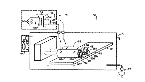
Figure 3 is a schematic diagram of the sputtering
system 50 using an AC power supply 52. For the reasons
discussed above, the AC power supply 52 preferably
20 produces a power signal with a frequency in the range of
lOkHz to lOOkHz. In a preferred embodiment, the fre-
quency of the AC power switch 52 is about 50kHz. Note
that the frequency of the power supply 52 is less than
the radio frequency range, so that reflected power is
25 not an important concern. The AC power supply 52 is
available from Halmar Robicon, ENI, Princeton Applied
Research, or Advanced Energy. The AC power supply 52 is
connected to transformer 54. Transformer 54 has a
bifilar-wound secondary 54b that prevents the secondary
30 54b from becoming an autotransformer. Transformer 54
may also have a grounded center tap 54a for safety. The
secondary of transformer 54 preferably has multiple taps
that provide the function of impedance matching for the
system. Transformer 54 is connected to a shunt capaci-
CA 02218279 1997-10-1~
W O96/34124 PCTrUS96/05588
tor 56. Shunt capacitor 56 helps start the plasma if it
extinguishes and reduces high-frequency noise. A typi-
cal value for shunt capacitor 56 is about 0.3 micro-
farad.
The impedance-limiting capacitor 58 is preferably
connected in series in the electrical path that goes
between the two targets through the transformer. In a
preferred embodiment shown in Figure 6, the impedance-
limiting capacitor 58'' is positioned in the secondary
winding of transformer 54''.
Looking again at Figure 3, as discussed above, the
capacitance of the impedance-limiting capacitor 58
prevents arcing in the sputtering system. The
impedance-limiting capacitor 58 limits the amount of
current that can flow between the targets in case of a
short. Impedance-limiting capacitor 58 is preferably a
large, variable capacitor. Capacitance values for the
impedance-limiting capacitor should be in the range of
about 0.2 to 10~F. Since the frequencies of the AC
power supply 52 are significantly lower than the radio
frequency power supplies, reflected power is not a prob-
lem, and therefore the capacitance 58 is not required to
avoid reflected power. The function of impedance
matching is accomplished with the multiple taps on the
secondary of the transformer as discussed above.
The AC power from the circuitry 59 is connected to
the cylindrical magnetrons 60 and 62. Cylindrical mag-
netrons are described in Wolfe et al. U.S. Patent No.
5,047,137 and McKelvey U.S. Patent No. 4,356,073, both
of which are incorporated herein by reference. The
cylindrical magnetrons are available from The BOC Group,
Inc., Airco Coating Technology Division, located in
Concord, California under the name C-MAG~. The
rotatable cylindrical magnetrons 60 and 62 use rotatable
cylindrical tubular targets 64 and 65. The cylindrical
_
CA 02218279 1997-10-1~
W O 96/34124 PCTnUS96105588
rotatable tubular targets 64 and 65 preferably comprise
~ an outer layer with a coat of a metallic or semicon-
ductor material. The semiconductor material layer is
- preferably doped so that the layer is more conductive.
Silicon is commonly used as the sputtered material in
cylindrical magnetron systems. The silicon can be reac-
tively sputtered to produce silicon dioxide or silicon
nitride layers on the substrate 80. Other typical di-
electric materials used include Tio2~ SnO2, Nb205, and
Al203.
The rotatable cylindrical magnetron includes magnet
assemblies 66 and 68. These magnet assemblies use mag-
nets 66a, 66b and 66c as well as 68a, 68b and 68c.
Since the magnet assemblies have three poles, they
produce two parallel cont~in ent areas. These contain-
ment areas form erosion zones when the target is acting
as the cathode.
The action of the targets 60 and 62 can be better
shown with respect to Figure 4. Figure 4 shows a cross-
sectional view of two cylindrical magnetrons 60' and62'. Cylindrical rotatable tubular targets 64' and 65'
are connected to the AC power supply shown in Figure 3,
so that the targets 64' and 65' alternate between being
the cathode (negative polarity) and anode (positive
polarity) of the s.ystem.
The magnet assembly 66 produces magnetic fields 90
and 92. The magnetic fields 90 and 92 contain the elec-
trons in the plasma when the magnetron 60' is acting as
the cathode so that the ions formed by the collisions
with the trapped electrons sputter off the target
material 64' in the erosion areas 94 and 96. In reac-
tive sputtering, the reactive ions combine with the
sputtering material either at the target, the substrate
or in the chamber atmosphere. The ions also remove the
dielectric material that has been redeposited onto the
CA 02218279 1997-10-1~
W O96/34124 PCTrUS96105588
surface of the cylindrical tubular target 64' outside
the two erosion zones 94, 96. When the polarity of the
power signal to the target 64' is reversed, the target
acts as an anode and attracts electrons. Because of the
5 rotation of the cylindrical tubular targets 64' and 65',
the portions of the targets 64' and 65' which were
eroded by the ions when the target acts as the cathode
are rotated into different positions away from the mag-
netic fields, such as magnetic fields 94 and 96. As the
10 cylindrical tubular target rotates, these cleaned areas
allow for the electrons to make electrical contact with
areas of the target away from the magnetic field. Addi-
tionally, since the targets 64' and 65' are cylindrical,
there is more area available for the electrons to
15 contact the targets 64' or 65' than in planar magnetron
systems. This lowers the system impedance.
In the system of the present invention, the targets
64' or 65' do not store charge since the dielectric
material has been eroded away. For this reason, there
20 is not as large a capacitance when the system is oper-
ating. Additionally, since charge is not stored onto a
dielectric material layer, the system of the present
invention is not likely to arc as a result of the
dielectric breakdown. This present sputtering system is
25 different from the prior art AC sputtering systems shown
with respect to Figure 2, since the dielectric layer 40
or 42 is deposited on top of target material and acts as
a capacitive element in this prior art system.
Looking again at Figure 4, in the preferred embodi-
30 ment, the distance between the cylindrical targets 98 isabout 1-3 inches, and the distance between the cylin-
drical targets in the wall 99a and 99b is about four or
more inches. These distances will ensure that the
recombination time for the plasma is shorter than the
35 time between positive and negative portions of the power
CA 02218279 1997-10-1~
W O 96/34124 PCTrUS96/05588
supply for a lOKHz ;n;mum frequency signal. The
arrangement of cylindrical magnetrons makes the plasma
relatively unaffected by the arrangement of the chamber
walls, since the discharge is maintained between the
targets.
Looking again at Figure 3, a gas supply 70 and pump
72 are used to supply the gases at the required pres-
sures for the sputtering deposition. Typical gases
include oxygen, nitrogen, and noble gases. Typical gas
pressures are 1-5 mTorr. The cathodes and power supply
are electrically isolated from the chamber. This may be
done by grounding the chamber at location 74. The sub-
strate 80 is coated by the sputtered dielectric materi-
al. This substrate 80 moves underneath the targets.
The line speed of the substrate 80, among other factors,
determines the deposition thickness of the dielectric
layer onto the substrate 80.
Figure 5 is a schematic diagram of an alternate
embodiment of the present invention. In this alternate
embodiment, only a single cylindrical magnetron 100 is
used. The other cylindrical magnetron is replaced by an
electrically conductive element 102. This electrically
conductive element is connected to the circuitry 59' to
supply the AC power supply to the cylindrical magnetron
and electrically conductive element. It is preferred
that the surface area of the electrically conductive
material 106 is equivalent to that of the cylindrically
rotatable target 104 on the cylindrical magnetron 100,
so that neither the cylindrically rotatable magnetron
100 nor the electrically conductive material 102
maintains a DC bias voltage.
Various details of the implementation and method
are merely illustrative of the invention. It will be
understood that various changes in such details may be
CA 02218279 1997-10-15
W O96/34124 PCTrUS96/05S88
within the scope of the invention, which is to be
limited only by the appended claims.
-