Note: Descriptions are shown in the official language in which they were submitted.
CA 02218392 1997-10-16
WO 96/33298 PCTIIJS96/04754
TITLE METHOD OF ELECTROPLATING A SUBSI~ATE,
ANP PRODUCTS MAPE THEREBY
BACKGROllND OF THE INVENTION
1. Field of the Invention
The present invention relates to methods of electroplating and to products made
thereby. In another aspect, the present invention relates to methods of electroplating a
co~ e metal onto a ~ul~ le, and to products made thereby. In even another aspect,
the present invention relates to methods of electroplating con~ ctors onto a seed layer
supported by a substrate, and to products made thereby. In still another aspect, the
present invention relates to mPthotle of clecL,oplating cc)n~ ctors onto a seed layer
~u~ol~ed by a diamond substrate, and to products made thereby.
2. Pescription of the Related A~t
It is the physical and chernical properties of natural ~i~mon~ls which render
o~ suitable for use in a wide range of applications. For example, natural diamonds
are the hardest substance known and exhibit low friction and wear properties.
Specifically, a natural dialllond's thermal conductivity, thermal diffusivity properties,
electrical resistivity and microhdl ~llle~ invite its substitution in various applications.
Specifically with respect to electronic applications, di~mon~, with a thermal
conductivity four times that of copper and a dielectric con~L~lL less than alumina or
~IIlmimlm nitride, has long been recognized as a desirable m~tPri~l for electronic
subsLl~es
It is likewise believed that ~li~mon~1 films would find utility in a broad range of
CA 02218392 1997-10-16
WO 96133298 PCT/US96/04754
electronic uses.
UllrulL-IlldLely, diamond films are not naturally occurring, but rather must be
m~nnf~c.tllred using any of a host of techniques. r
Fortunately, however, the physical and ch~mi~ l plop~l~ies of synthetic di~mon-lfilms have been found to be co-llpal~ble to those of bulk tli~mon~
For ~ r, it has been reported that electron assisted chemical vapor deposition
films have electrical resistivities greater than 10'3 Q-cm, microhardness of about 10,000
HV, thermal con~llctivity of about 1100 W m-l K-l, and thermal diffusivity of 200 to 300
mm2/s. These co"l~e favorably to those properties of natural diamond, i.e, resistivities
in the range of 107 to 102~ Q-cm, microhardness in the range of 8,000 to 10,400 HV,
thermal conductivity in the range of 900 to 2100 W m~l K-l, and thermal diffusivity of 490
to 1150 mm2/s. Thermal gravimetric analysis d~mn~ L~s the oxidation rates of diamond
films in air are lower than those of natural diamond. Additionally, it is reported that the
starting temperature of oxidation for microwave-assisted chemical vapor deposition
.li,.".~ l film is about 800~C, as evidenced by weight loss, while the morphology shows
visible oxidation etching pits at temperatures as low as 600~ C.
Thus, di~mc~n~l films also show promise for finding utility in a mllltit~l(le ofapplications, in~ lin~ electrical applications.
Currently, ~h~mic~l vapor deposition ~ n~l film has experienced limited market
entry primarily as heat sinks for laser diodes. However, there are many other industrial
uses planned for diamond film, virtually all of which require met~lli7~tion.
For example, diamond film substrates have been hailed as the only solution to
many of the thermal management problems currently encoullL~;Ied in the electronic and
optoelectronics par.k~ing area. As the packing density of electronic systems increases,
this thermal m~n~gemP.nt problem is only going to exacerbate. Met~lli7~tion of diamond
film s~tl~Les with highly con~ cting metals such as gold and copper is essPnti~l for these
applications. Some of the applications which are in dire need of the development of a
tenaciously adhering contluctinp~ metal film on a tli~monrl substrate include laser diodes
and diode arrays for telecommunications, power modules for on-board s~tellite~, high
powered microwave modules, MCMs, and especially 3-D MCMs.
CA 02218392 1997-10-16
WO 96/33298 PCTIUS96/04754
However, while the industry is in dire need of a tenaciously adhering (>lKpsi onpeel test) electroplated con-luctin~ metal film on a diamond substrate, the rhemir~1
inertness of rli~mond resists the formation of adherent co~ting~C on it. This is especially
true for large area (>lmm x lmm) diamond film subsLI~les and thick metal films (>2
microns).
P~esell~ly, met~lli7~ti~n is accomp1i~hed through some form of physical vapor
deposition. While this produces a high quality film, it also produces high m~tPri~l cost due
to its extreme waste of metal. Ele.,LIùpl~ g is prt;r~l~ble because is allows metal to be
deposited selectively, which would cut waste by over 90% from what is con~11med in a
physical vapor deposition process.
Physical vapor deposition processes are ~iUI i ell~ly the industry standard because
films deposited by such processes tend not to blister or peel at high temperatures. In a
physical vapor deposition process, the substrate is mounted inside a high vacuum~'.1".",1,~.i . The ~.llnlllh~l is evacu~te-l, and metal is either evaporated or sputtered to form
l 5 a coating on the sub~LI ~le. The ineffici~nr,y of the technique is due to the metal coating
that is deposited onto the rest of the vacuum cl ~lll~el at the same time. Only a small
xll~age of the metal that is consumed by the process lands on the substrate, with the
rest being lost.
Ele.illupl~ g would seem to be the proper ~n~ e for mrt~11i7ing rli~mnnt1 film
with gold. With cle~,llopl~Lillg, the plated metal is applied directly to the target, resulting
in much less waste as colllp~ed to physical vapor deposition. However, even though
cle~iLIopld~ has ~ nh1i~ d itself as a workhorse technology for cost effective thin film
and foil f~hrir~tion in the ele.;ll~ ~s industry, only sputtering and evaporation of gold and
copper have so far been collllnelcially s11r~ces~fi1lly utilized in m~t~lli7ing diamond film
s~sLI~les (and only on small substrates and only to small thirl~n~ses).
"Met~11i7in~ CVD Diamond For Electronic Applications", Iacovangelo et aL
Tntf~.m~tional Journal of Microelectronics And Electronics p~r~ging, Vol. 17, No. 3, at
252-258 (1994), discloses a physical vapor deposition technique for depositing a gold
layer onto a .1;, ~ film. As disclosed by Iacovangelo et al., thin gold films are applied
to metal seed layers on diamond films by either a spulleling process or a rhemi~ l vapor
CA 02218392 1997-10-16
WO 96/33298 PCT/US96/04754
deposition process.
As shown for coat numbers 11-13, the gold layers applied by the tearhings of
Iacovangelo et al. exhibit ~he~ n to the diamond substrate on the order of 4 to 10 Kpsi.
Unfortunately, the gold layers produced by Iacovangelo et al were on the order of 0.5
microns thin, too thin for use in most applications.
Iacovangelo et al., further disclose the electroplating of a triple layer of copper,
nickel and then gold onto a patterned thin film. However, as shown in Figure 4 of
Iacovangelo et al., this ele~,LIoplated layer is on the order of 200,~bm wide, far too narrow
for many applications. Electroplating onto diamond film substrates on the order of lcm
x 1 cm or larger requires that the problems induced by thermal stress be solved.Iacovangelo et al. do not disclose or teach how to electroplate onto larger
diamond film substrates in a manner sllfficiçnt to overcome the problems induced by
thermal stress. Biaxial stresses increase with h~creasillg diamond film size.
,~1rlition~l p~ with applying metal layers to ~ ,o~ films include blistering,
peeling and dçl~min~tion.
Therefore, there is a need in the art for a process for met~lli7in~ diamond and
other types of substrates which does not suffer from one or more of the prior art
limit~fion~
There is another need in the art for an ele-illoplating process for met~lli7in~
~ mnntl and other types of s~sLI ~Les which does not suffer from one or more of the prior
art limitations.
There is even another need in the art for an electroplating process for met~lli7ing
diamond and other types of substrates which provides a product with suitable adhesion
between the gold layer and the diamond film.
There is still another need in the art for an electroplating process for met~lli7ing
diamond and other types of subsL~Les which provides a product with suitable surface
ro~lghn~
There is yet another a need in the art for met~lli7ed diamond and other types ofsubstrates which do not suffer from the prior art limit~tion~
There is even still another need in the art for a met~lli7ed diamond and other types
CA 02218392 1997-10-16
WO 96/33298 PCT/US96/047~4
of substrates with suitable adhesion between the gold layer and the diamond film.
There is even yet another need in the art for a met~ 7ed diamond and other typesof substrates with suitable surface roughnPqq
These and other needs in the art will become appalenl to those of skill in the art
~ 5upon review of this spe~ific.~tion.
SUMMARY OF THE INVENTION
It is one object of the present invention to provide a process for met~lli7ing
mnn~1 and other types of sul,:,L, ~les which does not suffer from one or more of the prior
10art limitations.
It is another object to provide for an electroplating process for met~lli7.ing
mnntl and other types of s~ Lt;S which does not suffer from one or more of the prior
art limit~tiQnq.
It is even another object to provide for an electroplating process for met~lli7.ing
15diamond and other types of substrates which provides a product with suitable adhesion
between the gold layer and the rli~montl film.
It is still another object to provide for an electroplating process for mP,t~lli7in~
diamond and other types of substrates which provides a product with suitable surface
roughnPqq
20It is yet another object to provide for mets~lli7ed t1i~mon~1 and other tvpes of
substrates which do not suffer from the prior art limit~tionc
It is even still another object to provide for a met~lli7P,d diamond and other types
of substrates with suitable ~tlhP.cion between the gold layer and the ~ monrl film.
It is even yet another object to provide for a met~lli7P,d diamond and other types
25of substrates with suitable surface roughnesq.
These and other objects ofthe present invention will become appalelll to those of
skill in the art upon review of this specifiç~tion.
Accc l d;llg to one embodiment of the present invention there is provided a method
of electroplating an article having a surface with peaks and valleys, and articles made
theler.ol.. The method generally inc.llldçs electroplating a conductive metal onto the
CA 02218392 1997-10-16
WO 96/33298 PCT/US96/04754
peaks to cover the peaks with the conductive metal, and into the valleys to substantially
fill the valleys with the conductive metal.
According to another embodiment of the present invention there is provided a
method of ele~;llupldlil~g an article having a surface with a surface rollghneee, and articles
made Lllererlc,lll. The method generally inrllldes electroplating a conduct*e metal onto
the surface utilizing a current density less than or equal to J0, to form a conductive metal
layer having a surface ro~lghnees no greater than the article surface ro~lghnPeeAccording to even another embodiment of the present invention there is provided
a method of electroplating an article compnsing a supporting member and a seed layer
supl)c,l~ed by the sllp~ Lillg nlc;llllJt;l, with the seed layer having a surface with peaks and
valleys, and articles made therefrom. The method generally in~.llldes electroplating a
con-lllctive metal onto the peaks to cover the peaks with the conductive metal, and into
the valleys to substantially fill the valleys with the conductive metal.
Accold.l~ to still another embodiment of the present invention there is provideda method of electroplating an article comprising a supporting member and a seed layer
supported by the diamond member, with the seed layer having a surface with a surface
rou~hnPqe, and articles made therefrom. The method generally incllldee electroplating a
conrluctive metal onto the seed layer surface utili7ing a current density less than or equal
to J0, to form a con-luctive metal layer having a surface roughness no greater than the seed
layer surface ro~lghness.
Accol ding to yet another embodiment of the present invention there is provided
a method of met~lli7.ing a diamond film, and articles made therefrom. The methodgenerally in~.hldes a first step of applying a seed metal onto the diamond film to form a
seed layer having a surface ro~lghn.oee, with the seed layer having a surface with peaks and
valleys. The method further inrllldes ele~illoplalillg a conductive metal onto the peaks to
cover the peaks with the conductive metal, and into the valleys to substantially fill the
valleys with the conductive metal.
According to even still another embodiment of the present invention these is
provided a method of mP.t~lli7.ing a diamond film, and articles made therefrom. The
method generally in~ ldes applying a seed metal onto the diamond film to form a seed
CA 02218392 1997-10-16
WO 96/33298 PCT/US96/04754
layer, with the seed layer having a surface with a surface roughness. The method further
inr~ es electroplating a conductive metal onto the seed layer surface uti~ ing a current
density less than or equal to J0, to form a conductive metal layer having a surface
roughness no greater than the seed layer surface roughness
S According to even yet another embodiment of the present invention there is
provided a method of electroplating an article to form an electroplated layer having a
desired surface ro~1ghnçqc, and articles made thel~fiulll. The method generally inr.l1ld~c
(a) electroplating at a current density, a conductive metal onto the article to form an
electroplated layer. The method further inchlcles (b) detelllfilling the surface roughness
ofthe ele.iL,uplaLed layer. The method still further int~111(1es increasing the current density
of step (a) if the surface roughness determined in step (b) is less than the desired surface
roughness, and decreasing the current density of step (a) if the surface roughness
dt;~ e(l in step (b) is greater than the desired surface roughn~c~ This method may be
operated interactively until the desired surface roughn~cc is obtained for the thi~l~nes.c
required.
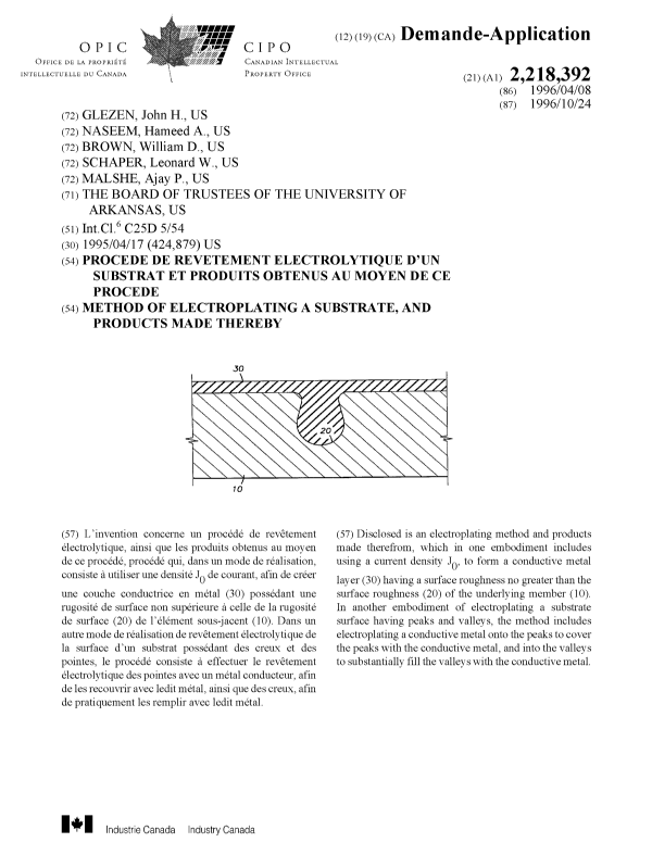
13RIEF DESCRIPTION OF THE DRAWINGS
FIGs. lA-C, show respectively, substrate 10 with irregularity 20 without an
ele~,LlùplaLed metal, substrate 10 with irregularity 20 ele~iLluplated over by electroplated
metal 30, and substrate 10 with irregularity 20 electroplated s~sL~lially filled by
electroplated metal 30.
DETAILED DESCRIPTION OF THE INVENTION
The present invention provides a method for electroplating a conductive metal
onto a target conductive metal layer surface, such that the formed electroplated metal
layer will have a resulting surface roughn~sc less than the initial surface roughn~sc of the
target layer.
~ The present invention also provides a method for ele~,LlùplaLillg a conductive metal
onto a target conductive metal layer surface, such that the formed electroplated metal
layer will have reduced likelihood of blistering away from the target layer at elevated
CA 02218392 1997-10-16
WO 96/33298 PCT/US96104754
temperatures, and will have good adhesion to the target layer.
The present invention generally in~ des a first step of met~lli7ing a supportingsubstrate to form a seed layer, followed by electroplating a conductive layer onto the seed
layer. Alternatively, the present invention may also be utilized to ele.;LIoplale a conductive
metal directly onto a conductive substrate even without a seed layer.
In the practice of the present invention, the substrate may comprise any material
that will be suitable for the desired application. Non-limiting examples of supporting
substrate m~t~.ri~l~ include metals, diamond, semiconductors, ceramics, thermoplastics or
thermosets.
Although much of the following description for the present invention makes
reference to tli~m~ntl film as the substrate, it is to be understood that this invention finds
applicability to any type of substrate.
The ~l;n~ films utilized in the practice of the present invention are well knownto those of skill in the art. The diamond films utilized in the present invention may be
made by any suitable process. G~nel~lly, such suitable methods of making diamond films
are generally ~h~ d as chemical vapor deposition techniques such as hot fil~m~ntDC arcjet, RF arcjet, microwave plasma, and microwave plasma jet methods.
Initial trç~tment of the supportin~ substrate
In the practice of the present invention, the supi)ol ~h~g substrate must generally
be cleaned to provide a proper surface for m~.t~lli7ing For example, with diamonds and
many metals, such cle~ning generally includes degreasing, removal of residual carbon, and
the removal of the cleaning solutions.
For 1 - n~ methods of cleaning a diamond film are well known to those of skill
in the art, and any suitable method may be utilized. Degreasing is generally accomrli~hed
by boiling the ~ mon~1 film in suitable chemical solvents, non limiting eY~mples of which
include trichloroethylene, acetone and alcohols. The removal of residual carbon is
generally accompli~h~od at slightly elevated temperatures ufili7ing an acid wash followed
by a base wash. As a non limiting ~ - r lei, residual carbon may be removed using sulfuric
acid/chromium trioxide at 160~C followed by ~,l.. ol-i~lm hydroxide/hydrogen peroxide
CA 02218392 1997-10-16
WO 96/33298 PCT/US96/04754
at 70~C. P~c~ c of these cle~nin~ solutions are then removed by subjecting the
diamond film to ultrasonic rlç~nin~ in deionized water.
In some applications, it will be necçcc~ry that the surface ro~ghnçss of the final
ele.iLluplaled con~lctive layer be quite low. For c,~ lc, many electrical applications will
S require the final electroplated conduct*e layer have a surface ro~lphnecc less than about
350 nm, ~ r~;~ly less than about 300 nm, and more pr~r~l~bly less than about 250 nm,
and most preferably less than about 200 nm. Of course, it is to be understood that the
present invention can be utilized to form a final electroplated conductive layer having
almost any desired surface ro~lghnçss.
The surface rol-ghnPcc ofthe underlying ~ul~ Le will tend to infll-~.nre the surface
rol-ghnrec ofthe final ele~illuplaLed conrl~ctive layer. It is generally plt;rt;;lled to start with
a substrate having a surface roughness near that desired in the final electroplated
con~ ctive layer. Likewise, the surface ro~-~hnecc of the seed layer on the substrate will
also tend to inflllçnre the surface ro--ghnrcc of the final electroplated con~l-lctive layer.
Thus, if a seed layer is utilized it is generally plt;rt;lled to utilize one having a surface
rol-ghnec.c near that desired in the final electroplated conductive layer.
Application of seed layer
Once the substrate is degreased and r.le~netl, the optional seed layer may be
applied. Methods of applying a seed layer to a substrate, especially a diamond film are
well known to those of skill in the art. In the practice of the present invention, the seed
layer may be applied using any suitable technique. In general, physical vapor deposition
methods are utilized to create the seed layers. Such techniques include sputtering
techniques, thermal evaporation, and electron-beam evaporation, and are well known to
those of skill in the art.
Apparatus for accomplishing physical vapor deposition are well known, and any
suitable appal~L~Is may be utilized in the practice of the present invention. Suitable
eql-ipmrnt inrl.ldrc a ~L~da--l thermal evaporator such as the Edwards E306A (Edwards
Colllpally, Great Britain) coating system.
According to the present invention, the seed layer may include one or more
CA 02218392 1997-10-16
WO 96133298 PCTIUS96/04754
subsurface layers. Optionally, the seed layer may further include a top surface layer of the
same metal as the metal to be electroplated onto the seed layer. Of course, any metal or
material that will adhere to the SI1IJ~O1 Liilg substrate, and provide a suitable surface for the
electroplated metal may be utilized. Non-limiting examples of materials suitable for use
as the seed layer(s) include ~ mimlm, copper, chromium, gold, nickel, niobium,
p~ll~tlillm, pl~timlm, silicon, t~nt~lllm~ il "." t~ln~t~n, and collll,illalions of any of the
rOI~goll~g
Titanium will tend to diffuse into gold. Therefore, if th~ni--m is utilized as asubsurface seed layer, a layer of pl~timlm or tlmg~t~n is generally utilized between the
tit~nil-m and gold layers.
With some metals, the seed layer will tend to be susceptible to de1~"il-,.l;on unless
the substrate is heated prior to and during the physical vapor deposition process. The
temperature is generally great enough to discourage del~min~tion of the final seed layer
but less than the degradation telll~el~L~Ire of the ~ mt)nfl film or the metal melting point,
whichever is less. For example, generally during the physical vapor deposition process
of depositing a chromium seed layer onto diamond film, the diamond film is heated to a
le,ll~ L~lre in the range of about 150~C to about 400~C. Preferably, the physical vapor
deposition process is carried out at a telll~el~L~Ire in the range of about 175~C to about
300~C, and most plerel~ly at a t~lllp~ L,lre in the range of about 1 85~C to about 225~C.
While various opc;l~ling pressures may be utilized, it is plt;r~;;ll ~;d that the physica
vapor deposition process for applying the seed layer is generally carried out at near
vacuum, on the order of about 6X10~ millibar or less, preferably on the order of about
lX10~ millibar or less. It is important that the vaporized chemical be thermally driven to
the target in a relatively unimpeded manner. Thus, it is n~cess~ry to create proper
conditions so that the vaporized çh~mic~l will have a high mean free path, on the order
of a m~ nihlde greater than the f~iet~nce between the ~hlomic~l target and the supporting
substrate.
Generally, the vacuum chamber is purged with nitrogen prior to obtaining the
vacuum, to remove substantially all oxidants.
In the practice of the present invention, the seed layer must have a relatively
CA 02218392 1997-10-16
WO 96/33298 PCT/US96/04754
perfect crystal structure, which structure can be infl~enced by the application rate. Low
seed layer application rates are utilized to provide a seed layer with the proper crystal
structure. Suitable application rates are on the order of 5-10~/sec or lower.
Electroplating a conductive layer
S Once the seed layer is in place, the cQn~1u~tive layer is applied onto the seed layers
ili7.ing an electroplating technique.
The inventors have determined that electroplating at low electroplating rates, RL~
utilizing low ele~ opla~ g current df~ne~ip~J JL~ will result in an ele-,~,ol)la~ed layer having
a surface roughnPcc less than that of the underlying layer upon which it is electroplated,
with roughness declc;a~illg with de~ ;d~illg RH and JH The inventors have also determined
that electroplating at high electroplating rates, RH~ utili7ing high electroplating current
dP.nCh;PC, JH~ will result in an electroplated layer having a surface roughnP,ss greater than
that of the underlying layer upon which it is electroplated, with roughn~ss increasing with
increasing RH and JH- An interme~ te electroplating rate R;" utili~ing an intermediate
current density J0, such that RL<RO<RH~ and JL<JO<JH~ will result in an electroplated layer
having a surface roughnP,,cs equal to that of the underlying layer upon which it is
electroplated.
The present invention thus provides a method of forming an electroplated layer
having a surface ro lghn~cc less than or equal to the surface roughness of the target layer,
by utilizing an electroplating rate less than or equal to RO, at interme~ te current density
less than or equal to JO.
The present invention also provides a method of forming an electroplated layer
having a target surface roughnPcc by monitoring the rou~hn.occ of the forming
el~,~,LIoplaled layer, and ,ll~lt;a~ing the elc~Lluplalillg rate and current density above RO and
JO, if the lllolllLoled roughn~cc is less than the target rou~hnesc, and by decreasing the
electroplating rate and current density below RO and ~ if the monitored roughn~cc is
greater than the target roughness.
The particular deposition rate or current density which will result in an
ele.,LIopldled layer having a roughn~cc greater than, less than or equal to that of the layer
upon which it is ele~illupldLed~ will vary accolding to the type of metal being electroplated,
= =
CA 02218392 1997-10-16
WO 96/33298 PCT/US96104754
12
the type of cle~iLI~lJlaLillg solution utilized, pH, solution density, bath te",pc;,~u,t:, anode-
to-cathode ratio, type of agitation, as well as other factors. It is generally nece~ ry to
conduct a simple test over a range of deposition rates or current densities to determine RO
and JO, and the ranges for RL~ JL~ RH and JH
For; r1~ when utilizing a certain colllllwl~ilally available gold plating solution,
it is generally nece.~ry to provide a current density at the anode of less than 1 mA/cm2
to provide an ele~iLI opla~ed layer having a surface ro~l~hn~e~ less than the roughness of the
underlying layer. Pl~:rt:l~bly, the current density at the anode will be in the range of about
0.001 to about 0.95 mA/cm2, more plert;l~bly in the range of about 0.01 to about 0.7
1 0 mA/cm2, even more preferably in the range of about 0.1 to about 0. 5 mA/cm2, and most
preferably in the range of about 0.1 to about 0.2 mA/cm2, to provide an electroplated layer
having a surface ro~ghnes.c less than the roughness of the underlying layer.
The surface of a substrate is not regular and may contain many irregularities,
which may be naturally occurring, an unwanted result of processing or h~n~11ing, or may
intentionally m~mlf~ tllred into the substrate (such as vias). As used herein, the
irregularity will be characterized as having a valley or low region, and peaks or high
regions.
An alternative electroplating embodiment of the present invention in~ ldes
electroplating a surface having surface irregularities such as crevices, cracks, grooves,
exposed microcavities, sc, ~lches, slits, slots, openings, hollow portions, cavities,
chambers, notches, pits, holes, vias, and/or voids. According to this alternative
embodiment, the electroplating is con~ cted such that the surface irregularity is
substantially filled by the electroplating process.
Rt;rt;,t;"ce is now made to FIGs. lA-C, which show It;~e-;Li~rely, substrate 10 with
irregularity 20 without an electroplated metal, substrate 10 with irregularity 20
electroplated over by electroplated metal 30, and substrate 10 with irregularity 20
substantially filled by electroplated metal 30.
While not wishing to be limited by theory the inventors believe that electroplating
over irregularities, as shown in FIG. lB will result in lower adhesion, and will provide
trapped electroplating solvents which will boil at elevated temperatures and blister the
CA 02218392 1997-10-16
WO 96/33298 PCT/US96/04754
article. The inventors also believe that the prior art electroplating methods generally
would ele~ opldLe over any surface irregularities, because at higher current d~.n~itie.~ the
electroplating charge would acc~-m~ te at the surface ofthe substrate, at peaks, and be
depleted at the bottom, or valley, of the irregularity. The inventors further believe that
lower current d~on~ities allow for the metal to substantially fill the irregularity, resulting in
better adhesion
Thus, the present invention in~ (ies electroplating a surface having surface
irregularities such as crevices, cracks, grooves, exposed microcavities, scratches, slits,
slots, openings, hollow portions, cavities, chambers, notches, pits, holes, vias, and/or
voids, to s~bst~nti~lly fill S~L~ILi~r all of the irregularities with the electroplated metal.
Plcrel~ly the volume of an irregularity is at least 50 percent, more plcrtlably at
least 80 percent, even more preferably at least 90 percent and even more preferably at
least 95 percent, still more preferably at least 98 percent, and most preferably at least 99
percent filled. Preferably at least 50 percent, more preferably at least 80 percent, even
more pl e rt;l ably at least 90 percent and even more ~1 ercl al)ly at least 95 percent, still more
~Icrcl~bly at least 98 percent, and most plere,~bly at least 99 percent ofthe irregularities
on the surface will be filled.
The proper ele-,lloplàLillg rate can be easily determined by varying the
electroplating rate over a range and analyzing the filling of the irregularities.
In the practice ofthe present invention, the electroplating is generally carried out
as follows. The supporting Illclllbcl with seed layer is co~ e~iled to a cathode and a
pl~tin--m plate connected to the anode. With the supporting member and platinum plate
submerged in an electroplating solution, a current is applied to drive the electroplating
process.
The process ofthe present invention finds utility in providing useful products for
use in electronic appli. ~linn~ The products ofthe present invention have utility in a broad
range of elecLI. ~, applicaLiolls, in~ ing sre~ifi~lly as diodes, flat panel displays, power
~mrlifi~rs, and as m--ltir.hir modules in general.
CA 02218392 1997-10-16
WO 96/33298 PCT/US96/04754
14
EXAMPLES
The following non-l~miting ~ l l~s are provided to further illustrate the invention
and are not meant to limit the invention in any manner. The following Procedures I-III
di.~c--cses the general method of preparing mP.t~lli7etl diamond film.
Procedure I
General Sample Pl epal ~lion
The r1i~mon-1 samples utilized in the Examples were lcm x lcm di~mon-l film,
produced by standard çhlo.mic.~l vapor deposition ("CVD").
De~l ~asillg the diamond film
The first step in sample pl~pal~Lion is degreasing, in which the diamond sample
is sequentially boiled in trichloroethylene, acetone and then mçth~nol.
The diamond sample is placed in 400 ml of trichloroethylene in a 600 ml Pyrex
beaker. Next, the beaker is placed on a standard hot plate inside a fume hood. By means
ofthe hot plate, the trichloroethylene is brought to a boil. A~er 15 mimltes, the ~i~mon~
film is removed from the boiling trichloroethylene. Unless otherwise specified, the
diamond sample is always handled ~ltili7in3~ metal tweezers and holding the diamond by
the edges.
The above procedures are next repeated with acetone. The diamond sample is
placed in 400 ml of acetone in a 600 ml Pyrex beaker. Next, the beaker is placed on a
standard hot plate inside a fume hood. By means of the hot plate, the acetone is brought
to a boil. After 15 mimltçs, the diamond film is removed from the boiling acetone.
The above procedures are next repeated with meth~nol. The diamond sample is
placed in 400 ml of mP.th~n~l in a 600 ml Pyrex beaker. Next, the beaker is placed on a
~L~da~d hot plate inside a fume hood. By means ofthe hot plate, the meth~nol is brought
to a boil. After 15 minllte~, the diamond film is removed from the boiling m.eth~nol.
Removal of residual carbon from the diamond film
3 0 1 gram of chromium trioxide powder is stirred into 400 ml of semiconductor grade
CA 022l8392 l997- l0- l6
WO 96133298 PCTIUS96/04754
sulfuric acid in a 600 rnl Pyrex beaker. Next, the beaker is placed on a standard hot plate
inside a fume hood. By means of the hot plate, the mixture of sulfuric acid/.,hloll-iu
trioxide powder is heated to 160~C. The diamond film is placed in the mixture for 30
min-ltes and then removed.
A similar procedure is repeated with a mixture of 200 ml of semiconductor grade
~"""o~ m hydroxide and 200 ml of hydrogen peroxide in a 600 ml Pyrex beaker. This
beaker is placed on a sL~ndald hot plate inside a fume hood. By means ofthe hot plate,
the mixture is heated to 70~C. The fli~monfl film is placed in the mixture for 30 minutes
and then removed.
Removal of residual cleaning solution
The diamond sample is placed in 600 ml of deionized water in a 600 ml Pyrex
beaker. The beaker is then placed inside a standard ultrasonic cleaner, with the fli~monrl
sample subjected to ultrasonic cleaning for at least three hours.
Procedure II
Pl e~al dlion of the seed layer
A seed layer was applied to the cleaned diamond film samples of Procedure I
utilizing an Edwards E306A coating system. The Edwards E306A is a standard thermal
evaporator, the operation of which is known to those of skill in the art, and which was
operated generally as follows.
Mounting of the diamond film samples
After venting the vacuum f~.h~mh.or with nitrogen gas, the bell jar is removed.
Removal ofthe bell jar provides access to and permits subsequent removal of the sample
holder, i.e. the metal plate at the top of the appal~lus under the jar. Next, one of the
screws in the sample holder metal plate is loosened, and a corner of the diamond film
sample is placed under the screw. The .li~ .i sample is oriented such that the substrate
side of the sample is against the plate, with the growth side of the sample facing out. The
~ 30 screw is then tight- nPd until the washer is snug against the holder, sufficiently tight to
CA 02218392 1997-10-16
WO 96/33298 PCT/US96/047~54
16
secure the sample when the plate is held upside down. The sample holder is then placed
in the evaporator. The piezoelectric holder is then placed in its standard position.
Mounting the chromium and gold targets
First, the center target holder, and two of the ~elipl~ l target holders on the
target holding appa~ s are loosened. Next, a standard ~hermal evaporation chromium
stick, commercially available from R.D. Mathis Company, is positioned with one end in
the center target holder, and the other end in one of the peripheral target holders. A
standard thermal evaporation molybdenum boat, also commercially available from R.D.
Mathis Company, is positioned with one end in the center target holder, and the other end
in the other peripheral target holder. To encourage good electrical connections, a small
metal shim is inserted between the molybdenum boat and washer of the center target
holder, and the chromium holder is rotated until the chromium target is in electrical
contact with the side electrode. Next, all the target holders are ti~htened to secure the
chroll~lll stick and the molybdenum boat. Finally, a small 2mm x 2mm x 2mm nugget
of gold of at least 99.99% purity is placed in the molybdenum boat.
Heater Adjllstment
For proper operation, it is nPcç~ry that the radiant heater is pointed at the
~ mnn~l film s~mpl~ that the thermnco-lple is close to the di~montl film samples, but not
shadowing any of them from the evaporating metal, and that the window on the radiant
heater is clear and not covered with metal.
Pumpdown
The rotary pump is Png~ged to pump down the vacuum chal,lbel until the Piranni
gauge reads 0.06 mbar. Next, the diffusion pump is ~ng~ged and filled with liquid
nitrogen. To protect the operator from exposure to the radiant heater, a cover is placed
over the bell jar. The radiant heater is set to 200~C and ~ng~ed Over the next few
hours, the diffusion pump is operated to take the pressure in the vacuum chamber down
to 6E-6 mbar.
CA 02218392 1997-10-16
WO 96/33298 PCT/US96/04754
Thermal evaporation of the seed layer
The thermal e~/~ol~lor is first operated to form a chro~ lll layer directly on the
diamond film, and then operated to form a gold layer on the clll on~iulll layer.First utili~in~ the chromium stick as the target, the current is increased until a
chromium deposition rate of 0.5 to 1.0 nm/sec is achieved, to form a chromium layer from
17.5 nm to 22.5 nm thick. Subsequently, the target holding ap~ L~Is is rotated so that
the gold nugget in the molybdenum boat is now the target. The current is increased until
a gold deposition rate of 0.5 to 1.0 nrn/sec is achieved, to form a gold layer from 275 nm
to 325 nm thick.
Once the clll~llliulll and gold layers are formed, the current is stopped, the
SU~ e heater is turned off, the tliffil~ion pump is ~ Png~ge~l, and the chamber is vented
once. The chamber is pumped down again, but with the roughing pump instead of with
the rlifl;l~ir~n pump. The apparatus is then allowed to cool at room te;llllJel~Lule for about
an hour, at which time the chamber is again vented, and the seed layer coated diamond
film removed.
Procedure III
Plepal~lion of gold layer
Diamond film samples from Procedure II having a chromium and gold seed layer
are utilized in this Example.
800 ml of a sulfite-based, non-toxic gold electroplating solution, available from
r,.~Pl~ d is utilized in a 1500 ml Pyrex beaker. The solution must be tested to make sure
its operational pal~llelt;l~ are within tolerances. The pH, which must be between 10.5
and 11, is ill,l~ased with KOH and dew~ased with DI water. The density, which must be
between 12~ Baume ("Be") and 16~Be, is increased with gold concentrate from
Englehard, and decreased with DI water.
During the electroplating operation, the solution is ~git~ted by means of a
m~gnP,tir. stirbar, and the solution temperature is ~ ;..Pd between 55~C and 60~C by
means of an electrical hot plate.
The ~l;~,.. ~n~ sarnple is ~tt~-~hed to the cathode ~llig~tor clip, and a pl~tim-m plate
CA 02218392 1997-10-16
WO 96/33298 PCT/US961047~4
18
(2" x 2") is ~tt~rhrd to the anode alligator clip. Only about S cm2 of the anode is placed
into the solution. A standard HP power supply which provides current measurable to a
tenth of a milli~mp is utilized.
The electroplating is cnn~lucted at a current of 0.5mA, which sets the current
density at the cathode to 0.5 mA/cm2, to provide a deposition rate of about 0.4 microns
gold/hr. The electroplating is continued until the desired thiçL-nrs~ of gold is obtained.
Procedure IV
Peel Test Procedure
The plated diamond films from Procedure III are tested using the "Peel Test"
procedure of ASTM B-571 (11), except that an ~lllmimlm test strip is substituted for the
steel or brass strip. The equipment utilized was a Seb~ti~n III tester.
The non ele~ uplaLed (back) side of the diamond film is secured to an ~lllmimlm
b~.kpl~te using J.B. Weld epoxy. An alllminllm pull strip is secured to the electroplated
(front) side of the ~ monll film using J.B. Weld Epoxy. A metal clip is utilized to press
the pull strip against the sample. The sample is then allowed to cure at 1 50~C for 3 hours,
and at room Lel..~ L~Ire for 21 hours. The Sebaefi~n III tester is then utilized to provide
a pulling force at a pulling angle 90~ to the surface of the film, to pull the ~lnmimlm pull
strip off of the diamond film. The digital display will indicate the force with which the
m~rhine was pulling when the pull strip was removed. By dividing this force value by the
area of the pull strip, it can be reported in pounds per square inch.
Example 1
Control At Hi~h Deposit Rate
A lcm x lcm diamond sample was coated with a seed layer of 200A chromium
and 3000A gold by Procedures I and II as shown above. Seven gold layers were then
applied at various current densities utili~ing Procedure III above at the parameters as
shown in Table 1 below.
CA 02218392 1997-10-16
WO 96/33298 PCTIUS96/04754
19
Table 1
Layer No. Current Density Ek,~ u~Jlal;llg Layer Thickness Total Thickness Deposit
(mA/cm~) time (min) (~m) (!lm) Rate
(llm/hr)
" I 5.6 0.5 0.3 0.3 36
2 5 1 0.4 0.7 24
3 10 2 0.8 1.5 24
4 10 2 0.5 2.0 15
4 1.0 3.0 15
6 10 2 0.5 3.5 15
0 7 10 2 0.5 4.0 15
Peel Test of Procedure IV was con~ cted on the above 7 layer sample: sample
peeled at 20 pounds (350psi).
Examl~le 2
Control At High Deposit Rate
A l cm x l cm diamond sample was coated with a seed layer of 200A chromium
and 3000A gold by Procedures I and II as shown above. A 4.5 ~lm gold layer was applied
at a deposition rate of 18 ~m/hr utili7ing Procedure III. Peel Test results utili~ing
Procedure IV was as follows: peeled at 251bs (440 psi).
Example 3
Rou~hnçss vs. Deposit Rate
Two lcm x lcm 11;," ". ~ samples "A" an "B" were each coated with a seed layer
of 200A chlo1l~-1 and 3000A gold by Procedures I and II as shown above. Eight layers
of gold were then deposited on each seed layer by Procedure III above, with surface
rol l~nP.~ measured initially and af[er deposition of each gold layer. Results are presented
in Table 2.
CA 02218392 1997-10-16
WO 96133298 PCT/US96/047~;4
Table 2
Cumulative layer Current Density at Deposition rate F~nn~hn.~.cg
;. L ,.~ c~ (~m) anode (mA/cm2) (~bm~r) (nm)
SAMPLE"A"
0 N/A N/A 150
1.3 5 20 350
1.6 0.5 0.1 232
1.9 0.5 0.1 200
2.0 0.5 0.05 187
2.2 0.5 0.07 162
2.3 0.5 0.05 140
4.0 1.8 0.6 221
SAMPLE "B"
0 N/A N/A 145
1.3 5 20 350
1.6 0.5 0.1 240
1.9 0.5 0.1 246
2.0 0.5 0.05 212
2.2 0.5 0.07 180
2.3 0.5 0.05 190
4.0 1.8 0.6 230
Example 4
Annealing of seed layer
3 lcm x l cm diamond samples "C" were each coated with a seed layer of 200A
chromium and 3000A gold by Procedures I and II as shown above. 3 l cm x l cm rii~mnn~l
samples "D" were each coated with a seed layer of 200A chromium and lOOOA gold by
Procedures I and II as shown above, and an additional 2000A gold by Procedures I and
CA 02218392 1997-10-16
WO 96133298 PCT/US96/047~i4
21
II as shown above, except that an deposition temperature of 50~C was utilized.
For samples C-l and D-1, the seed layer was not ~nn~le~l, for sample C-2 and D-
~, 2, the seed layer was ~nn~le~l at 300~C, and for s~mrles C-3 and D-3, the seed layer was
~nn~led at 400~C. All samples were then electroplated with a 5A thick gold layer at 0.8
J' SmA/cm2 by Procedure III above.
These six ele.,l,~?laLed samples were all subjected to anns~lin~ at 350~C. Finally,
all samples were subjected to the Peel Test of Procedure IV. Results are shown in the
following Tables 3-6.
10 Table 3
Surface Rol-~hness
Of Seed Layer Before Electroplating (nm)
SAMPLES C SAMPLES D
1 (SEEDLAYERNOT 250 250
ANNEALED)
2 (SEED LAYER 254 269
ANNEALED AT 300~C)
3 (SEED LAYER 262 288
ANNEALED AT 400~C)
Table 4
Surface Roughness
25Of Electroplated Gold Layer (nm)
SAMPLES C SAMPLES D
1 (SEED LAYERNOT 181 206
ANNEALED)
2 (SEED LAYER 183 233
ANNEALED AT 300~C)
3 (SEED LAYER 150 207
ANNEALED AT 400~C)
CA 02218392 1997- 10- 16
Wo 96/33298 PCT/US96/047S4
22
Table 5
Surface Roughness Of Electroplated
Gold Layer - After Annç~lin~ At 350~C (nm)
SAMPLES C SAMPLES D
1 (SEED LAYER NOT 180 213
ANNEALED)
2 (SEED LAYER 180 230
ANNEALED AT 300~C)
3 (SEED LAYER 250 450
ANNEALED AT 400~C)
Samples in the bottom row blistered, accounting for the high surface ro-lghn~es
Tablç 6
Peel Test Results (PSI)
SAMPLES C SAMPLES D
1 (SEED LAYER NOT 2400 (epoxy broke) 2900
ANNEALED)
2 (SEED LAYER ANNEALED 2900 (limit of peel tester) 2900
AT 300~C)
3 (SEED LAYER ANNEALED 33 0
AT 400~C)
Example 5
Thermal Stress and Thermal Cycling
Of Large Samples (21mm x 21mm)
21mm x 21mm samples were each coated with a seed layer of 200A chrol"iu"l and
3000A gold by Procedures I and II as shown above. Seed layers were subjected to no
~nn~lin~, ~nn~ling at 350~C, or ~nn~linF~ at 400~C. A gold layer of 5A was then
deposited on the seed layer of each sample by Procedure III above. One set of samples
was then subjected to thermal stress (~nn~lin3~) at 350~C or 400~C for 30 mim-t~
CA 02218392 1997-10-16
WO 96/33298 PCT/US96/04734
Another set of samples was then subjected to thermal cycling from 150~C to -65~C, in
close agreemt;l~l with military standards. The samples were subjected to 16 cycles, with
a cycle as follows: climbing to 150~C in 15 mimltc~, dwell for 15 mimlte.~, down to -65~
in 15 minlltes, dwell for 15 mimltes This procedure varied from standard military
sperifir,~tion~ in that 15 minute L~ re ine~ llLs were utilized instead of 10 minute
in.,l~",e"L~.
Table 7
Peel Testin~ After Thermal Cyclin~ (PSI)
SAMPLES For Thermal SAMPLES For The~nal
Stress Cycling
l(SEEDLAYERNOT 350~C:3600 3600
ANNEALED) 400~C:2000
2 (SEED LAYER ANNEALED 350~C: 3600 3600
AT300~C) 400~C: 1800
3 (SEEDLAYERANNEALED 350~C:0 0
AT400~C)
Example 6
21mm x 21mm s~mples of tli~montl were degreased and cleaned according to
Procedure I above. The teaching~ of Procedure II were followed to deposit the seed
layer, except that the thickness of chromium was always 300 ang~L,~J",s, and copper was
deposited instead of gold. The copper was deposited to a thic.1~n~ of 2000 angstroms,
but at varying substrate temperatures. Also, the base pressure in the thermal evaporator
cl~"l~el was varied. Also, the te"lpe,~L.lre ofthe seed layer anneal step was varied. All
of the samples were then electroplated with cooper to a thic~ness of 8-10 microns. All
ofthe samples were then anne~le~ at 350~C. All ofthe samples were then observed for
blisters.
CA 02218392 1997-10-16
WO 96/33298 PCT/US96/04754
24
Table 8
SAMPLE EVAPORATION EVAPORATION SEED LAYER BLISTER
SUBSTRATE BASE PRESSURE ANNEAL RATING
TEMPERATURE (MBAR) TEMPERATURE
(~C) (~C)
1 200 1.3E-6 AMBIENT MEDIUM
2 200 1.3E-6 300 MEDIUM
3 200 1.3E-6 400 MEDIUM
4 Cr: 200 1.3E-6 AMBIENT LOW
Cu: 50 1 .SE-7
Cr: 200 1.3E-6 300 LOW
Cu: 50 1 .5E-7
6 Cr: 200 1.3E-6 400 VERY LOW
Cu: 50 1 .SE-7
7 Cr: 200 1.3E-6 AMBENT HIGH
Cu: 50 1 .SE-7
8 Cr: 200 1.3E-6 300 HIGH
Cu: 50 1.5E-7
9 Cr: 200 1.3E-6 400 N/A (etched
Cu: 50 1.5E-7 off)
While the illustrative embodiments of the invention have been described with
particularity, it will be understood that various other modifications will be appalelll to and
can be readily made by those skilled in the art without departing from the spirit and scope
of the invention. Acc~ldillgly, it is not intP.nrled that the scope of the claims appended
hereto be limited to the examples and descriptions set forth herein but rather that the
claims be construed as encompa~ing all the features of p~tent~hle novelty which reside
in the present invention, in~ tlin~ all features which would be treated as equivalents
thereof by those skilled the art to which this invention pertains.