Note: Descriptions are shown in the official language in which they were submitted.
~ . CA 022l8~02 lss7-l0-l7
, f
AC INPUT CELL INTENDED FOR DATA ACQUISITION CIRCUITS.
Subject of the invention.
The present invention relates essentially to an
AC input cell intended for data acquisition circuits,
more particularly in railway applications.
Technical background.
Currently, AC input cells intended for data
acquisition circuits essentially consist of mechanical
safety relays which are connected together by simple
cabling.
Objects of the invention.
The present invention aims to provide a cell
for AC inputs intended for data acquisition circuits,
particularly in railway applications, which has at
least equivalent behaviour in terms of safety to that
of the prior art, while keeping inherent advantages of
compactness, easier maintenance and fitting as well as
greater longevity.
More particularly, the present invention aims
to provide a cell in which misreading always errs on
the side of safety.
The present invention also aims to detect
malfunctions which may occur in the various constituent
elements of the cell.
The present invention furthermore aims to
minimize the influence of a variation in the
characteristics of the components which are used, under
the effect of an external factor such as a rise in
temperature, for example.
Principle characteristics of the present invention.
The present invention relates to an AC input
cell intended for data acquisition circuits, comprising
at least one device for detecting a voltage greater
than the reference for the positive half-cycle at the
input voltage, and a device for detecting a voltage
greater than the reference for the negative half-cycle
of the input voltage.
CA 02218~02 1997-10-17
: l 2
Each of these detection devices comprises a
Zener diode, an optocoupler comprising an emission LED,
a diode and a resistor, these elements being arranged
in series.
According to a first preferred embodiment of
the present invention, the elements constituting each
of the two detection devices mentioned above are
arranged on one branch, the two branches being arranged
in parallel.
In this case, the elements constituting the
detection device for the negative half-cycle are
arranged in a configuration which is the opposite to
that of the ones constituting the detection device for
the positive half-cycle.
lS According to another embodiment, the two
detection devices are arranged in series on a single
branch. In this case, the elements constituting the
detection device for the negative half-cycle are
mounted in a configuration which is the opposite to
that of those constituting the detection device for the
positive half-cycle.
Particularly advantageously, a resistor is
arranged in parallel on each of the optocouplers, so as
to make it possible to limit the influence of the
leakage current of the Zener diodes.
Brief description of the figures.
The present invention will be described in more
detail with the aid of the following figures:
Figures 1 and 2 represent outline diagrams which
show the essential elements
constituting a device according to
the present invention.
Figure 3 represents an embodiment of the
device according to the present
invention implemented by applying
the principles described in figures
1 and 2.
CA 02218~02 1997-10-17
Description of some preferred embodiments of the
invention.
In order to understand the principles
underlying the design of the device according to the
present invention, reference will be made essentially
to Figures 1 and 2 which incorporate the principle
characteristic elements.
The device according to the present invention,
commonly referred to as an AC input cell for data
acquisition circuits, as represented in Figure 1 is
essentially composed of two branches, referred to as
branches A and B, which respectively comprise a device
~or detecting a voltage higher than the reference for
the positive half-cycle at the input voltage (branch A)
and a device for detecting a voltage higher than the
reference for the negative half-cycle of the input
voltage (branch B).
In general, the voltage thresholding is carried
out by measuring the time for which, during one half-
cycle, the input voltage is greater than the reference
voltage. If this time is greater than the predefined
limit time, then the input voltage is considered as
sufficient; otherwise, it is considered that there is
not a sufficient voltage at the input.
The branches A and B comprise the same
elements, but arranged in an opposite configuration.
The branch A, which constitutes the detection device
for the positive half-cycle, comprises a Zener diode
DZ1, an optocoupler U1, a diode D2 and a resistor R1,
these elements being arranged in seriesi whereas the
branch B which constitutes the detection device for the
negative half-cycle comprises a Zener diode DZ2, an
optocoupler U2, a diode D4 and a resistor R3, also
arranged in series but in the opposite configuration.
According to a preferred embodiment,
represented in Figure 2, it is conceivable for all the
elements represented on the branches A and B in Figure
1 to be arranged on a single branch, the two series of
elements - Zener diode DZ1, optocoupler U1 and Zener
. CA 022l8~02 lss7-l0-l7
,
- 4 -
DZ2, optocoupler U2 - being arranged in opposite
configurations.
The main drawback of this configuration
described in Figure 2 resides in the fact that the
Zener diodes DZ1 and DZ2 may have a particularly large
leakage current which increases with temperature.
Advantageously, in order to solve this problem,
a resistor R7 or R13 is arranged in parallel on the
LEDs of the optocouplers U1 and U2.
It is also conceivable for another element,
having the same function, to be arranged in parallel
with U1 or U2. However, a resistor seems to be the
element with the most reliable and simplest design.
This device has the essential advantage of
obtaining current thresholding.
Another advantage of this arrangement is a
saving in volume and an increase in sa~ety.
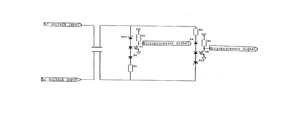
Figure 3 describes a practical example of a
device according to the present invention, using the
principles described in Figure 2.
The device described in Figure 3 is a 110 volt
- 50 hertz AC input cell, essentially comprising 3
functional units arranged in cascade.
The first unit (unit I) essentially makes it
possible to limit overvoltages.
The second unit (unit II) guarantees
consumption of the input power.
The third unit (unit III) performs the voltage
thresholding of the cell, as well as the DC isolation
between the input and the output processing lines.
The unit I consists of a varistore VR1, a
resistor R5, diodes and spark gaps with a view to
protecting the cell ~rom overvoltages, whereas the unlt
II which ensures the minimal rated consumption
(reactive power) consists of a "4 terminal" capacitor
C4 coupling the input terminals of the cell to the unit
III which itself provides the voltage thresholding.
The varistore VR1 clips the overvoltages
occurring during differential discharges, while the
CA 02218~02 1997-10-17
resistor R5 limits the amplitude of the current peaks
in the "~ terminal" capacitor C4 during the discharges,
as well as the dV/dt.
The "4 terminal" capacitor C4 should be
designed so as to ensure minimal consumption for a
given 50 hertz input voltage.
The device for detecting a voltage higher than
the reference for the positive half-cycle of the input
voltage, this device being located on branch A,
essentially consists of the elements described in
Figures 1 and 2: the Zener diode DZ1, the optocoupler
U1, the diode D2 and the resistor R1, while the device
for detecting a voltage higher than the reference for
the negative half-cycle of the input voltage, which
device is located on branch B, essentially consists of
the same elements as the ones described in Figures 1
and 2: the Zener diode DZ2, the optocoupler U2, the
diode D4 and the resistor R3.
Furthermore, a fuse F1 or F2 is present in each
of the branches A or B.
The principle selection criterion for the two
main optocouplers U1 and U2 is that of operating with
the lowest possible LED current, in order to make it
possible to dissipate the minimum amount of power in
the series resistors R1 and R3. This also makes it
possible to minimize the contribution of the
characteristic of the emission LED in the value of the
voltage threshold.
The conduction time of the optocouplers U1 and
U2 is measured by sampling, 32 times at regular
intervals of 20 milliseconds (therefore corresponding
to a frequency of 50 hertz), the electrical level
delivered to the output processing lines and by
counting the number of samples for which there is a
logic state "0".
The emission LED of U1 emits throughout the
time when the input voltage is higher than the
threshold voltage of the branch A. The emission of this
LED of the optocoupler U1 entails earthing of the
~ ~ = ~
CA 02218~02 1997-10-17
resistors R2, R9 and R10 arranged in "pull up" on the
optocoupler U1, thus leading to Ql being turned off and
to the reading of a "0" logic level on the input of the
multiplexer scanned by the processing line A (Ql
emitter).
The emission LED of U2 emits throughout the
time when the input voltage is higher than the
threshold voltage of the branch B. The emission of this
LED of the optocoupler U2 entails earthing of the
resistors R4, R11 and R12 arranged in "pull up" on the
optocoupler U2, thus leading to the reading of a "0"
logic level on the input of the multiplexer scanned by
the processing line B (collector of the output
transistor of U2).
There are two safety criteria guaranteed for
110 volt AC input cells:
- the detection threshold must not fall below a
limit for a 50 hertz sinusoidal voltage;
- the power consumed under a 50 hertz sinusoidal
voltage for an input in the logic state 1 cannot
fall below a second limit value.
It should be noted that, apart from the 4
terminal capacitor, the components used to produce an
AC input cell have no other intrinsic guarantee of
safety. For this reason, safety needs to rely on the
use of the redundancy and checking the coherence of the
data provided to the processing lines.
In particular, processing line A scans the
voltage on the emitter Ql, while line B is connected to
the collector of the output transistor of the
optocoupler U2. At the end of each scanning cycle, A
and B exchange, for mutual verification purposes, their
own value for the number of samples taken when U1 or U2
were conducting.
The useful signals at the output of the cell
are naturally presented on the collectors of the output
optocouplers with a high output impedance level for the
"1" electrical state and a low impedance level for the
"0" electrical state. One precaution then consists in
CA 02218~02 1997-10-17
using, just for the processing line A, a buffer stage
with transistor inverting the level of the output
impedances so that there is this time a low impedance
level for the "1" electrical state and a high impedance
level for the "0" electrical state.
This characteristic has the risk of producing
an "OR" logic function (as regards the state of the
inputs) for the two processing lines in the event of
defects consisting in the occurrence of a short-circuit
between the output signals of the various cells.
This buffer stage consists of the transistor Q1
and the resistor R6 which are placed in the processing
line A.
By thus creating an asymmetry between the two
lines, in the event of multiple parasitic conducting
circuits occurring, possibly affecting the same cells
for the two processing lines, the following behaviour
is profited from: the equivalent of a wired OR function
(at the electrical level) is produced on the cells of
line A, while the equivalent of a wired AND (at the
electrical level) is produced on the cells of line B.
This leads to a divergence between processing
lines being detected as soon as the two cells affected
by the parasitic conducting circuits are in different
states.